Ultrafast spatiotemporal control of photocarriers in doped semiconductors
Author E Laine Wong
Degree Conferral Date
2018‑07‑31
Degree Doctor of Philosophy Degree Referral
Number
38005甲第18号 Copyright
Information
(C) 2018 The Author
URL http://doi.org/10.15102/1394.00000589
Okinawa Institute of Science and Technology Graduate University
Thesis submitted for the degree Doctor of Philosophy
Ultrafast spatiotemporal control of photocarriers in doped semiconductors
by
E Laine Wong
Supervisor: Keshav M. Dani
July, 2018
Declaration of Original and Sole Authorship
I, E Laine Wong, declare that this thesis entitled Ultrafast spatiotemporal control of pho- tocarriers in doped semiconductors and the data presented in it are original and my own work.
I confirm that:
• No part of this work has previously been submitted for a degree at this or any other university.
• References to the work of others have been clearly acknowledged. Quotations from the work of others have been clearly indicated, and attributed to them.
• In cases where others have contributed to part of this work, such contribution has been clearly acknowledged and distinguished from my own work.
• None of this work has been previously published elsewhere, with the exception of the following:
Publication:
E Laine Wong, Andrew J. Winchester, Vivek Pareek, Julien Madéo, Michael K. L.
Man and Keshav M. Dani. Pulling apart photoexcited electrons by photo-inducing an in-plane surface electric field. Science Advances (Accepted).
Patent:
ii
Declaration of Original and Sole Authorship iii E Laine Wong, Michael K. L. Man and Keshav M. Dani. Ultrafast control of pho- toexcited particles with high spatial resolution. US Provisional Patent Application Number: US 62/660,818.
Date: July, 2018 Signature:
Abstract
Ultrafast spatiotemporal control of photocarriers in doped semi- conductors
Control of the spatial and temporal dynamics of photoexcited charge carriers at the sur- faces and interfaces of semiconducting materials is pertinent to many of modern technolo- gies such as solar cells, photodetectors and other optoelectronic devices. In inhomoge- neous materials such as nanostructured materials, spatial variations in carrier dynamics are inherent via the material design and accordingly allow for improvements in device performance e.g. transport of electrons from donor to acceptor regions in photovoltaic devices. On the other hand, one can also create spatial inhomogeneity in the carrier dynamics in homogeneous systems by using a non-uniform photoexcitation profile. This would have the advantage that the control of the carrier dynamics could be more flexible and not tied down to the fixed material design. In principle, photoexcitation even with a simple Gaussian beam could result in nontrivial inhomogeneous carrier dynamics within the full-width-half-maximum (FWHM) of the optical spot. However, in typical ultra- fast spectroscopy measurements performed thus far, one averages out the photocarrier response over the excitation spot and spatial variations therein are inaccessible.
In this thesis, we create nontrivial spatiotemporal dynamics of the photoexcited elec- trons in a homogeneous Zn-doped GaAs using the spatial intensity variation in a simple Gaussian photoexcitation beam. We image these dynamics using time-resolved photoe- mission electron microscopy (TR-PEEM) - a technique offering both high temporal and
iv
Abstract v spatial resolutions. In particular, we demonstrate the spatial redistribution of the pho- toexcited electrons in two different regimes: (I) the early time delays where we control the vertical transport of electrons to the sample surface and (II) at long time delays where we manipulate the lateral distribution of the electrons along the sample surface.
In the first study, we achieve spatial variations in the screening process of the intrinsic surface field, which influences the vertical drift of photoexcited electrons from the bulk to the sample surface. Combined with the occurrence of Auger recombination in regions of higher intensity, we see a depletion in the electron population at the center, with a gain just away from the center. We show control of these processes and how they affect the electron distribution on the sample surface in nontrivial ways.
In the second study, we show that at long time delays the spatially varying screening process leads to the creation of lateral fields along the sample surface. These highly local and spatially varying lateral fields then act upon the photoexcited electrons, eventually pulling them apart into two distinct distributions. Using a simple model that explains the experimental data, we also show the possibility of generating near-arbitrary lateral fields and thus controlling electrons on the sample surface in more general ways.
In conclusion, this thesis demonstrates the capability to create and control nontrivial spatiotemporal dynamics of the photoexcited electrons even in a homogeneous semicon- ductor by exploiting the intensity variation of an ultrafast light pulse. This capability could lead to a promising new handle for use in high-speed optoelectronic devices.
Acknowledgement
First of all, I would like to express my sincerest gratitude to Professor Keshav Dani for his continuous support, guidance and patience throughout the many years of my PhD research in OIST. I have learnt a great deal from him, both in terms of research as well as the necessary soft skills for a successful career later in life. Next, I would like to express my sincere thanks to Professor Bala Murali Krishna Mariserla and Dr. Michael Man Ka Lun for their immense help and support on the HHG setup and the PEEM instrument, and for their invaluable advice and discussions on the topics. My sincere thanks also go to Dr. Julien Madéo, Andrew Winchester and Vivek Pareek for their help and the many insightful discussions on my research projects. A special thanks to Yumi-san for all her help throughout the years with the administrative dealings. I would also like to express my heartfelt gratitude to the past and present staffs at the Student Support Section for making me feel welcome and at home since my very first day in Okinawa and for their continual support throughout my stay in OIST and in Okinawa.
vi
To my parents Wong Yoon Sim & Tan Kim Choo
Contents
Declaration of Original and Sole Authorship ii
Abstract iii
Acknowledgement v
Contents vii
List of Figures x
List of Tables xii
Outline 1
1 Imaging the distribution and flow of photocarriers 3
1.1 Chapter overview . . . 3
1.2 Study of spatiotemporal dynamics of photocarriers . . . 3
1.2.1 Why study spatiotemporal dynamics? . . . 3
1.2.2 How to study spatiotemporal dynamics? (Overview) . . . 4
1.3 Techniques to study spatiotemporal dynamics of photocarriers . . . 5
1.3.1 Ultrafast pump-probe microscopy . . . 5
1.3.2 Scanning ultrafast electron microscopy . . . 6
1.3.3 Time-resolved photoemission electron microscopy . . . 7
viii
Contents ix
1.4 Chapter conclusion . . . 7
2 Time-resolved photoemission electron microscopy 8 2.1 Chapter overview . . . 8
2.2 Photoemission electron microscopy . . . 8
2.2.1 Introduction . . . 8
2.2.2 Theory of operation . . . 10
2.2.3 Light sources for PEEM . . . 12
2.3 Time-resolved photoemission electron microscopy . . . 15
2.3.1 Bringing in time resolution through optical pump-probe technique . 15 2.3.2 Previous studies with TR-PEEM . . . 15
2.4 Chapter conclusion . . . 17
3 Experimental setup & sample preparation 18 3.1 Chapter overview . . . 18
3.2 TR-PEEM optical layout . . . 18
3.3 Sample preparation & characterization . . . 22
3.3.1 Sample preparation . . . 22
3.3.2 Existence of surface states . . . 23
3.3.3 Optical penetration depth of the pump and probe pulses . . . 24
3.3.4 Space charge effect . . . 25
3.3.5 Confirmation of conduction band . . . 26
3.3.6 Beam spot size measurement . . . 28
3.3.7 Temporal resolution of TR-PEEM . . . 28
3.3.8 Determination of photocarrier lifetime . . . 31
3.4 Chapter conclusion . . . 31
4 Controlling the vertical transport of photocarriers 33 4.1 Chapter overview . . . 33
Contents x
4.2 Experimental method . . . 34
4.3 Inhomogeneity of physical processes within the full-width-half-maximum . 34 4.4 Verification of vertical transport and Auger recombination . . . 36
4.5 Controlling the spatiotemporal dynamics of photocarriers . . . 40
4.6 Impact upon electron distribution profile . . . 42
4.7 Chapter conclusion . . . 48
5 Separation of photoexcited electrons with ultrafast light pulse 49 5.1 Chapter overview . . . 49
5.2 Experimental method . . . 50
5.3 Ultrafast separation of like charges . . . 50
5.4 Controlling the degree and rate of separation . . . 52
5.5 Formation of lateral electric field . . . 54
5.6 Dipole model & numerical simulation . . . 56
5.7 Chapter conclusion . . . 59
Conclusion 61
Bibliography 64
List of Figures
2.1 Schematic of Brüche’s 1st PEEM system . . . 9
2.2 Schematic of an energy diagram for the photoelectric equation . . . 10
2.3 Schematic of a spectroscopic photoemission and low energy electron micro- scope . . . 11
2.4 Band structure & Brillouin zone . . . 14
2.5 Previous studies with TR-PEEM . . . 16
3.1 Schematic of the ultrafast pump-probe setup for TR-PEEM measurement . 20 3.2 PEEM main measurement and auxiliary chambers . . . 22
3.3 LEED & PEEM measurements of sample surface . . . 23
3.4 Surface bands bending in p-type GaAs . . . 24
3.5 Schematic illustrating the extent of the optical penetration depths relative to the depletion width of the space charge region . . . 25
3.6 Photoemission spectra showing no observable space charge effect . . . 26
3.7 TR-ARPES of p-type GaAs <110> surface along theΓ-L direction at 0ps time delay . . . 27
3.8 Determination of photoexcitation spot size . . . 29
3.9 Determination of TR-PEEM setup temporal resolution . . . 30
3.10 Determination of the photocarrier lifetime . . . 31
4.1 Spatial inhomogeneity in the photocarrier dynamics within the FWHM . . 35
xi
List of Figures xii 4.2 Controlling the relatives sizes of the two contrasting regions by fine-tuning
the photoexcited carrier densities . . . 37 4.3 Screening dynamics of the photocarriers as a function of the photoexcited
carrier density . . . 38 4.4 Photocarrier dynamics at low and high carrier densities . . . 39 4.5 Spatial variation in the local carrier dynamics for the intermediate carrier
density of 8.4 x 1018cm−3 . . . 41 4.6 Spatial variation in the local carrier dynamics for an intermediate carrier
density of 6.2 x 1018cm−3 . . . 43 4.7 Spatial variation in the local carrier dynamics for an intermediate carrier
density of 7.6 x 1018cm−3 . . . 44 4.8 Spatial variation in the local carrier dynamics for an intermediate carrier
density of 9.3 x 1018cm−3 . . . 45 4.9 From rapid broadening to shrinking of the spatial distribution profile of
electrons . . . 46 5.1 Puling apart photoexcited electrons within the pump spot . . . 51 5.2 2D images showing the separation of the photoexcited electrons along the
short axis of the elliptical pump spot for high carrier density of 2.1 x1019cm−3 52 5.3 Controlling the degree and rate of separation of the photoexcited electrons 53 5.4 Layer of surface dipoles before and after photoexcitation . . . 54 5.5 Spatially inhomogeneous partial screening of the intrinsic surface field for
photoexcited carrier density of 7.0 x 1018cm−3 . . . 55 5.6 Schematic of laterally varying surface potential due to the non-uniform
screening of the intrinsic surface field . . . 56 5.7 Formation of in-plane spatially varying electric field . . . 58 5.8 Numerical simulation of the evolving lateral electric field and the electron
distribution profile for the photoexcited carrier density of 2.1 x 1019cm−3 . 59
List of Tables
4.1 Single exponential fit of the rise time of time-delayed photoemission signals for low carrier densities . . . 38
xiii
Outline
This thesis is organized as follows:
Chapter 1 describes the rising need for a single probing method that combines high spatial and temporal resolutions for the study of carrier dynamics in semiconductors. It then briefly examines the spatial and temporal scale required to access the photocarrier dynamics within the photoexcitation spot. The chapter then goes on to discuss the strengths and weaknesses of three newly developed techniques that have been showing great potential for the study of charge carrier dynamics in semiconductors with both high spatial and temporal resolutions.
Chapter 2 describes in further detail time-resolved photoemission electron microscopy (TR-PEEM) that is used for the studies described in this thesis. The chapter first looks at the operating principle and the light sources available for a photoemission electron microscope. It then goes on to provide a brief overview of the previous studies conducted using TR-PEEM.
Chapter 3 describes in detail the setup of the ultrafast pump-probe spectroscopy used and the introduction of the ultrafast pulses into the electron microscope. The second part of this chapter covers the preparation and characterization of the Zn-doped GaAs sample.
This is then followed by a discussion of the optical and electronic properties of the sample that are crucial to the understanding of the experimental results presented in Chapter 4
1
Outline 2 and Chapter 5.
Chapter 4 first demonstrates the inhomogeneous photocarrier dynamics within the FWHM of the photoexcitation spot. The chapter then discusses the spatial variation in the partial screening of the intrinsic surface field and the Auger recombination that results in the depletion of electrons near the center of the spot and the vertical drift of electrons to the surface further away from the center. It is then demonstrated that the ratio between the two spatial regions of influx and depletion of electrons can be controlled via tuning the photoexcitation intensity. Lastly, the impact of the inhomogeneous photo- carrier dynamics on the spatiotemporal distribution of the electrons at the sample surface is discussed.
Chapter 5 first presents the experimental data showing the eventual separation of the photoexcited electrons within the optical spot into two resolvable distributions. The chap- ter then demonstrates the control of the degree and rate of separation of the charge carriers via the spatial profile and the intensity of the photoexcitation beam. The chapter then goes on to provide both an intuitive and a quantitative model to explain the underlying charge transport phenomena and to reproduce the salient features of the experimental data.
Chapter 1
Imaging the distribution and flow of photocarriers
1.1 Chapter overview
This chapter briefly discusses the motivation to study the photoexcited charge carrier dynamics at the surfaces of semiconductors with simultaneous high spatial and temporal resolutions. The chapter then briefly examines the pros and cons of three emerging techniques with the desired high spatial and temporal resolutions followed by a brief overview of the studies that have been successfully carried out with these techniques.
1.2 Study of spatiotemporal dynamics of photocarriers
1.2.1 Why study spatiotemporal dynamics?
The spatial and temporal dynamics of photoexcited charge carriers at the surfaces and interfaces of semiconductors is of vital importance to the proper design and performance of many modern technologies such as solar cells, photocatalytic processes and other opto- electronic devices. For example, the length scale of the transport of hot carriers in hybrid perovskite thin film might be key to improving the efficiency of solar cells [1]. In the
3
Imaging the distribution and flow of photocarriers 4 case of photocatalytic processes, the efficient separation of the photoexcited electron-hole pairs and the transport of the charge carriers to the material surfaces are amongst the few rate determining steps of the redox reactions [2]. As such, manipulation of the spa- tiotemporal distribution of the charge carriers at the material surfaces could potentially allow for temporally-controlled photocatalytic activities to happen at selected spatial locations. Even for homogeneous semiconducting materials, spatial variation in the pho- tocarrier dynamics can be induced by harnessing the rich variety of intensity-dependent physical processes that can occur in semiconductors. The capability to manipulate the spatial and temporal distribution of the photocarriers within the optical spot by utilizing the non-uniform photoexcitation intensity profile could potentially lead to the control of photocarriers beyond the diffraction limit of light. The continual development of these scientific and technological aims necessitates the development of techniques that are ca- pable of imaging the photocarrier dynamics with simultaneous high spatial and temporal resolutions.
1.2.2 How to study spatiotemporal dynamics? (Overview)
The natural timescale of electron dynamics such as thermalization, scattering and re- combination largely falls between the nanosecond to femtosecond range i.e. 10−9−10−15 seconds. To measure such a short burst of event, one would require an even faster probe.
To date, ultrafast pump-probe spectroscopy remains one of the widely used technique to access such transient dynamics. With this technique, an ultrafast pump pulse is used to first excite the sample and a time-delayed probe pulse is used to monitor the pump-induced change in the optical properties of the sample. The temporal dynamics of the photoexcited charge carriers can then be inferred from the change in the measured transmission or re- flection of the probe pulse as a function of the time delay between the arrivals of the pump and the probe pulses. The temporal resolution of this technique is typically only limited by the laser pulse duration which is in the range of 10s – 100s of femtoseconds. Despite the success of pump-probe spectroscopy in unveiling many important physical phenomena
Imaging the distribution and flow of photocarriers 5 in semiconductors, its nature of bulk averaging the measured quantities renders it inapt for the study of spatially inhomogeneous dynamics nor photocarrier transport.
Microscopy techniques, on the other hand, are often used to image spatially vary- ing structures and motions in molecular and biological samples. The spatial resolution required for the study of photocarrier dynamics in semiconductors is typically in the mi- cron to nanometer scale. The vast selection of commercially available optical and electron microscopes with the desired spatial resolution has aided in the fruition of several new techniques that interfaces the pump-probe spectroscopy with the microscopy techniques to allow for the study of photocarrier dynamics with simultaneous high spatial and tem- poral resolutions. In the following section, the strengths and weaknesses of three such techniques i.e. ultrafast pump-probe microscopy, scanning ultrafast electron microscopy and time-resolved photoemission electron microscopy will be further discussed in details.
1.3 Techniques to study spatiotemporal dynamics of photocarriers
1.3.1 Ultrafast pump-probe microscopy
Ultrafast pump-probe microscopy is an all-optical technique that extends the functionality of a conventional ultrafast pump-probe spectroscopy with the use of an optical microscope.
Compared to the other two techniques, this technique is comparatively easy to setup and does not require any ultrahigh vacuum system. This technique retains the femtosecond temporal resolution of the pump-probe spectroscopy while also offering high spatial res- olution of a few hundreds of nanometers. To track the motion of the charge carriers, the probe beam is scanned across the region-of-interest relative to the position of the pump beam. Similar to pump-probe spectroscopy, the charge carrier dynamics is indirectly in- ferred from the measurement of the photo-induced change in the optical properties of the sample. This technique has allowed researchers to reveal the heterogeneous charge carrier
Imaging the distribution and flow of photocarriers 6 dynamics within single nanorod [3] and perovskite grains [4], as well as to study the drift and diffusion phenomena in semiconductor nanostructures [5, 6, 7] and perovskite thin films [1, 8].
1.3.2 Scanning ultrafast electron microscopy
Scanning ultrafast electron microscopy (SUEM) combines the spatial resolution of a scan- ning electron microscope (SEM) with the temporal resolution of an ultrafast pump-probe setup. In contrast to the optical-pump-optical-probe of the ultrafast pump-probe mi- croscopy technique, SUEM is an optical-pump-electron-probe technique that utilizes an ultrafast electron packet to probe the photocarrier dynamics. The shorter wavelength of the electron probe naturally provides for a higher spatial resolving power. The temporal resolution is however limited to a few picoseconds due to the duration of the secondary electron emission process [9]. SUEM tracks the local populations of the photoexcited electrons and holes by raster scanning the electron probe across the sample surface and measures the photo-induced enhancement or suppression of the secondary electron yield at each locations. Due to the short escape depth, only the secondary electrons from the top few nanometers of the sample are emitted to vacuum and detected, making SUEM a surface sensitive technique. The interpretation of SUEM measurements can be quite complex due to the many factors that can affect the secondary electron emission. For example, the higher average energy of the photoexcited electrons leads to an increase in the secondary electron emission. On the other hand, the presence of the photocarri- ers also leads to an increased scattering of the secondary electrons thus suppressing the secondary electron emission. A comprehensive review of the working principle and the contrast mechanism of SUEM can be found in [9]. The high spatiotemporal resolution of SUEM has enabled researchers to study the extent of charge carrier separation in a silicon p-n junction [10], the anomalous diffusion regime and spontaneous electron-hole pair separation in an amorphous silicon sample [11], as well as the anisotropic diffusion of hot holes in black phosphorus [12].
Imaging the distribution and flow of photocarriers 7
1.3.3 Time-resolved photoemission electron microscopy
Time-resolved photoemission electron microscopy (TR-PEEM) interfaces a photoemission electron microscope with an ultrafast pump-probe setup. In contrast to the two techniques described in the previous sections, TR-PEEM maintains the femtosecond temporal res- olution of a pump-probe setup while also exploiting the high spatial resolving power of an electron microscope. In addition, TR-PEEM is also a non-scanning technique thus allowing for fast image acquisition. To study the photocarrier dynamics, TR-PEEM uses an optical pump to photoexcite electrons into the conduction band and a time-delayed optical probe to photoemit the photoexcited electrons from the sample. The photoemit- ted electrons are then collected by the electron microscope to form a series of images that reflect directly the time-delayed spatial distribution of the photoexcited electrons in the sample. Due to the low electron energy, typically in the range of a few electronvolts, only the electrons from the top few nanometers of the sample will be photoemitted, making TR-PEEM a surface sensitive technique. Further details of the TR-PEEM technique and a brief overview of the previous studies carried out using this technique will be discussed in Chapter 2.
1.4 Chapter conclusion
The first part of this chapter described briefly the motivation for investigating the photo- carrier dynamics in semiconductors with simultaneous high spatial and temporal resolu- tions. It then looked at the timescale and spatial resolution required for the studies and the current techniques used i.e. pump-probe spectroscopy and microscopy, for achieving the desired temporal or spatial resolution. The second part then compared the strengths and weaknesses of three emerging techniques that combine the temporal resolution of the pump-probe spectroscopy with the spatial resolution of the microscopy technique. The next chapter will describe in further details the TR-PEEM technique that is used for the studies in this thesis.
Chapter 2
Time-resolved photoemission electron microscopy
2.1 Chapter overview
This chapter starts with a brief introduction to photoemission electron microscopy (PEEM).
It then describes the working principle and the available light sources for PEEM. This is then followed by a brief overview of the previous studies conducted using TR-PEEM.
2.2 Photoemission electron microscopy
2.2.1 Introduction
In 1933, with the use of a simple magnetic lens, Brüche first demonstrated that electrons produced via ultraviolet light irradiation and accelerated to high energy could be used for surface imaging (Figure 2.1) [13]. In the following years, this simple instrument was continually improved upon with the inclusion of additional electron lenses, contrast aper- tures and ultrahigh vacuum systems [13,14,15]. Today’s PEEM is typically capable of a lateral spatial resolution of better than 15nm as demonstrated by Elmitec PEEM III [16].
An overview of the milestones of PEEM development can be found in [14, 15].
8
Time-resolved photoemission electron microscopy 9
Figure 2.1: Schematic of Brüche’s 1st PEEM system [13]
PEEM is a variant of surface electron emission microscopy that is widely used in the studies of surfaces, thin films and nanostructures. Contrary to most electron emission microscopes, PEEM images the sample surface with photoelectrons that are generated by an ultraviolet (UV) or an x-ray light source, as depicted in Figure 2.1. This technique provides information about the electronic structures, chemical and structural composition of the local environment being probed based on Einstein’s photoelectric equation of
hν =φ+EB+EKE (2.1)
where
hν is the energy of incident photon φ is the work function of the sample EB is the core level binding energy
EKE is the kinetic energy of the photoelectron
With photon irradiation, there are three potential imaging candidates i.e. photoelec- trons, secondary and Auger electrons. Photoelectrons are electrons that are photoemitted directly from the sample by the incident photons. Due to the low photon energy (4.65eV) used for the studies in this thesis, the main imaging candidate is the photoelectrons as any
Time-resolved photoemission electron microscopy 10
Figure 2.2: Schematic of an energy diagram for the photoelectric equation
additional energy loss from inelastic scatterings will leave the electrons with insufficient energy to overcome the work function of the sample. The following subsection will go on to discuss the theory of operation behind PEEM and the different light sources available for PEEM imaging.
2.2.2 Theory of operation
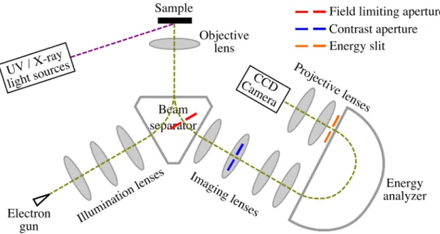
Our PEEM instrument is a spectroscopic photoemission and low energy electron micro- scope (SPELEEM) (Figure 2.3) that is also equipped with an electron illumination arm that provides for the capability to perform low energy electron imaging (LEEM) and diffraction (LEED) measurements. As shown in Figure2.3, both LEEM and PEEM share the same imaging column, differing only in the illumination columns. For PEEM, the illumination column is as simple as shining a UV or an x-ray light onto the sample.
The imaging column, on the other hand, comprises at least three lenses i.e. objective, intermediate and projective lenses, as well as an energy analyzer [17]. The objective lens collects, accelerates and focuses the emitted photoelectrons to the first image plane in the beam separator. The objective lens together with an angle-limiting aperture are the
Time-resolved photoemission electron microscopy 11
Figure 2.3: Schematic of a spectroscopic photoemission and low energy elec- tron microscope
two factors that typically determine the overall resolution and the transmission of the system. The angle-limiting aperture, also known as the contract aperture is located at the diffraction plane after the beam separator. The introduction of the contrast aperture by Boersch in 1942 [13] aids in reducing the spherical and chromatic aberrations of the objective lens and thus achieving better resolution by transmitting only near incidence photoelectrons.
By tuning its focal plane, the intermediate lens places either the image plane or the diffraction plane at the entrance of the energy analyzer thus allowing PEEM to switch between real space or reciprocal space imaging. The energy analyzer together with an energy-selection slit placed at its exit, determines the energy resolution of the system, which is nowadays achievable in the ∼100meV range [18]. The projective lens then mag- nifies the image or the diffraction plane at the exit of the analyzer onto a detector that is made up of a microchannel plate, a fluorescent screen and a CCD camera. As the emitted photoelectrons are accelerated to high energy, all the lenses used are either electrostatic or magnetic lenses instead of optical lenses. Similar to the imperfection in the physical shape of an optical lens, electron lenses also suffer from astigmatism. As such, stigmators
Time-resolved photoemission electron microscopy 12 and deflectors are incorporated into the imaging column to correct for such irregularities.
2.2.3 Light sources for PEEM
Gas discharge lamps
The first PEEM setup by Brüche in the 1930s came years before the first functional laser was built in the 1960s. Back then, mercury lamp fluorescence provides the necessary photons for PEEM applications. However, the wide energy distribution of the mercury lamp greatly limits the resolution of the microscope, rendering PEEM unable to compete with the thermionic emission electron microscope that had successfully surpassed the resolution of light microscope in 1942 [14]. This limitation is eventually overcome with the advent of two additional light sources for PEEM i.e. synchrotron radiation and frequency- multiplied laser source.
Synchrotron radiation
As a relativistic electron travels in a circular trajectory, it experiences a radial accel- eration and emits an electromagnetic wave tangent to its trajectory. In a synchrotron facility, magnetic structures such as bending magnets, wigglers and undulators are used to accelerate electrons in a curved path for the generation of a wide spectrum of elec- tromagnetic waves with high brilliance. Today’s synchrotron facilities typically cover the electromagnetic spectrum from the extreme ultraviolet (EUV) to the hard x-ray regimes and are capable of generating high brilliance beam with an average brightness of 1020photons/s/mrad2/mm2/0.1%BW [19]. The wide spectral range and the high photon flux make synchrotron radiation a strong candidate for PEEM imaging. In addition, the new generation of synchrotrons is now capable of producing femtosecond pulses, adding high temporal resolution to PEEM imaging. However, such capability is still limited to only a handful of facilities. Furthermore, synchrotron facilities are generally large-scale operations with high overhead cost, are space-consuming, and are typically shared by
Time-resolved photoemission electron microscopy 13 multiple research groups worldwide thus limiting beam time accessibility.
Table-top frequency-multiplied laser source
Frequency-multiplied laser source, on the other hand, is laboratory-based and thus has smaller footprint, significantly lower operation cost, and much less conflict over beam time availability. To date, many of the femtosecond lasers found in laboratory settings utilize titanium-doped sapphire (Ti:sa) crystal as their gain medium due to its wide gain bandwidth that allows for the generation of ultrashort pulses. These Ti:sa lasers have a wide range of wavelength tunability ranging from 1100nm to 650nm that is equivalent to the photon energy range of approximately 1 – 2eV. This energy range is considerably low for the photoemission of electrons from most materials whose work functions typically lie within the range of 4 – 6eV. Conveniently, the high intensity achievable by femtosecond lasers allows for the generation of light with higher photon energy through nonlinear frequency conversion processes.
There are two mechanisms for the generation of higher frequency light. One of the mechanisms is via nonlinear frequency conversion in nonlinear crystals. Nonlinear crystals are materials that exhibit strong nonlinear polarization response to the electric field of the driving laser as described by the following equation:
P(t) = ε0χ(1)E(t) +ε0χ(2)E2(t) +ε0χ(3)E3(t) +... (2.2)
Materials with high χ(2) nonlinearity are often used for nonlinear frequency conversion processes such as second harmonic generation and sum frequency generation. Beta barium borate (BBO) is one of these nonlinear crystals that possesses the required high χ(2) coefficient and is widely used for the generation of the second, third and fourth harmonics of Ti:sa lasers. This mechanism is comparatively easy to implement and offers high conversion efficiency e.g. 40% conversion efficiency for the second harmonic generation of 800nm with a BBO crystal. The high conversion efficiency allows for the generation
Time-resolved photoemission electron microscopy 14
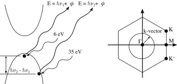
Figure 2.4: Band structure & Brillouin zone The schematic illustrates PEEM’s access to different parts of the band structure and the Brillouin zone of a sample depending on the incident photon energy.
of higher frequency light with sufficient photon flux even at MHz repetition rate. The use of a high repetition rate light source minimizes space charge effect in the imaging column and allows for shorter image acquisition time for PEEM measurements. On the flip side, the main drawback of this mechanism is the transparency limit of the BBO crystal that is ∼190nm (6.5eV), below which the crystal becomes highly absorptive. The low photon energy, barely higher than the work functions of most materials, limits the access of PEEM to electrons from the upper part of the valence band as well as from within a small region of the Brillouin zone centering around the Γpoint, as illustrated in Figure 2.4.
The second mechanism for generating higher harmonic orders of the fundamental laser frequency is via nonlinear interaction of an inert monatomic gas with an intense laser field of the magnitude of 1013−1015 W/cm2. The energy of the photons generated is typically much higher than the work function, φ, of most materials and thus is capable of photoemitting electrons from deeper within the band structure (Figure2.4). Furthermore, the k-space that can be imaged with these photons could easily cover the entire Brillouin zone of most materials thus allowing the study of physical processes happening at the high k-vectors. The main drawback of this mechanism is its low conversion efficiency of
Time-resolved photoemission electron microscopy 15 10−3−10−6 that necessitates either a high power laser with an average power of >80W [20] or a sophisticated enhancement cavity [21] to attain reasonable photon flux at MHz repetition rate.
As the band gap of GaAs lies at the Γ point, the generation of high frequency light using nonlinear crystals is the preferred mechanism due to its simplicity. In addition, as we are only interested in the photoexcited electrons, low energy photon is preferred to avoid photoemitting the electrons from the valence band which could potentially overwhelmed the signal or lead to space charge effect.
2.3 Time-resolved photoemission electron microscopy
2.3.1 Bringing in time resolution through optical pump-probe technique
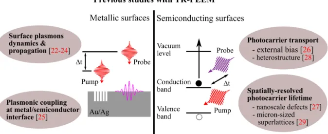
With the imaging probe pulse in place, the inclusion of an ultrafast pump pulse and a delay stage to provide for the pump-probe delays are the logical next step to bring in the desired temporal resolution to the PEEM measurements via a pump-probe setup. As de- scribed in the previous chapter, the time-delayed photoemission of the photoexcited elec- trons allows TR-PEEM to image directly the photocarrier spatiotemporal distributions with high resolutions. Using TR-PEEM, various plasmonic processes on nanostructured metallic surfaces as well as the transport and recombination of photocarriers on semi- conducting surfaces have been investigated as discussed in further details below (Figure 2.5).
2.3.2 Previous studies with TR-PEEM
The potential of time-resolved imaging was first realized experimentally in 2005 for the study of surface plasmon dynamics in a nanostructured silver film [22]. The simultaneous spatiotemporal imaging has allowed Kubo et al. to observe the quantum interference of
Time-resolved photoemission electron microscopy 16
Figure 2.5: Previous studies with TR-PEEM. The schematic illustrates the use of TR-PEEM for the study of surface plasmons at metal/vacuum and metal/semiconductor interfaces as well as photocarrier transport and recombination in semiconductors.
the localized surface plasmons polarization waves [22]. Since then, this technique has enabled the study of coherent interaction between localized surface plasmons (SPs) and propagating surface plasmon polaritons (SPPs) [23], the imaging of SPPs propagation and interference at their native wavelength [24], and the understanding of the mechanism of hot electron generation at the interfaces of metallic nanoparticles and a semiconducting substrate [25].
Apart from the studies of various plasmonic processes on metallic surfaces and nanos- tructures, the potential of TR-PEEM in imaging the photocarrier dynamics in semi- conductors has also been successfully demonstrated in recent years [26, 27, 28, 29]. In contrast to metallic surfaces, imaging of semiconducting surfaces is inherently more chal- lenging due to the higher material resistivity. For the generation of high energy photon to overcome the material work function (typically 4 – 6eV), a kHz amplifier system is generally preferred to attain sufficient photon flux of the3rd and4thharmonics. However, the use of a kHz system is also likely to result in a local buildup of the space charge as well as sample charging due to the higher number of photoemitted electrons per pulse and the higher material resistivity. On the other hand, though the use of a 80MHz oscillator
Time-resolved photoemission electron microscopy 17 system minimizes the space charge effect and leads to better signal-to-noise ratio, the pulse energy is typically too low to generate sufficient flux of the high energy photons.
By careful optimization of the laser pulse fluence and repetition rate, Fukumoto et al.
demonstrated in 2014 the capability of TR-PEEM to image the photocarrier transport [26] and nanoscale defect recombination [27] on a semiconducting surface. Since then, TR-PEEM has been used to study the generation and transport of photoexcited electrons in a InSe/GaAs heterostructure [28] and to measure the lifetimes of micron-sized twisted graphene superlattices [29].
2.4 Chapter conclusion
The first part of this chapter described the main components of a spectroscopic photoe- mission and low energy electron microscope. It then went on to discuss the advantages and disadvantages of the different light sources available for the photoemission electron microscope. The second part of the chapter briefly discussed about the additional chal- lenges in using TR-PEEM to image semiconducting surfaces. In contrast to metallic surfaces, semiconductors typically have higher sample resistivity which could result in sample charging as well as space charge effect. Hence, careful balancing of the need for high repetition rate system and the need for high pulse energy is critical for TR-PEEM imaging of semiconducting samples. The next chapter will describe in further details the optical layout of the pump-probe setup, its coupling into the PEEM measurement chamber as well as the preparation and characterization of the GaAs sample.
Chapter 3
Experimental setup & sample preparation
3.1 Chapter overview
As mentioned in the previous chapter, time-resolved photoemission electron microscopy (TR-PEEM) is a technique that combines the femtosecond temporal resolution of an ultrafast pump-probe spectroscopy with the nanoscale spatial resolution of a photoemis- sion electron microscopy. The first part of this chapter will describe the optical layout of the ultrafast pump-probe setup as well as its operation together with the photoemis- sion electron microscope. The second part of this chapter will cover the preparation and characterization of the sample to ensure a pristine surface. Some additional optical and electronic properties of the sample that are pertinent to the understanding of the experimental results will also be discussed here.
3.2 TR-PEEM optical layout
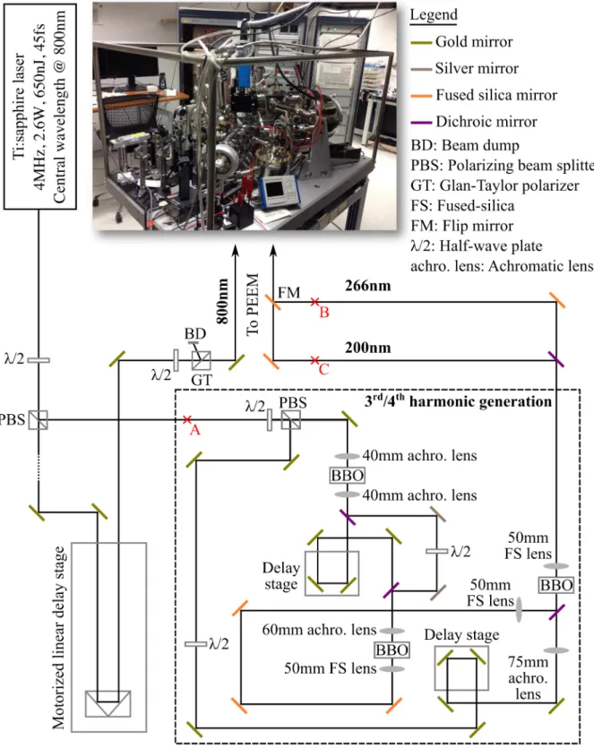
The laser system i.e. F EM T OSOU RCET M scientif icT M XL is a high energy Ti:sapphire oscillator system. XL runs at a repetition rate of 4MHz with pulse energy of 650nJ and
18
Experimental setup & sample preparation 19 outputs 45fs pulses at a central wavelength of 800nm. As shown in Figure3.1 , the 800nm output beam is split into two paths i.e. the pump and the probe paths, via the use of a half wave plate and a polarizing beam splitter. The 800nm pump beam is directed towards PEEM while the probe beam is directed towards a third and fourth harmonic generation setup (dashed box in Figure 3.1) for the generation of 4 – 6eV photon energy.
A motorized linear delay stage in the pump beam path provides the time delay between the arrival of the pump and the probe pulses at the sample.
The new 3rd and 4th harmonic generation setup (originally built by Vivek Pareek) follows the generation scheme as demonstrated in [30] and utilizes achromatic lenses to achieve a much better (circular) spatial beam profile, a higher conversion efficiency for the harmonic generation, and easier day-to-day alignment than the previous setup used in [28]. For the harmonic generation, the 800nm probe beam is first split into two paths: one to be used as a fresh 800nm beam for the 4th harmonic generation later while the other is used for the generation of both the 2nd and the 3rd harmonics. For the 2nd harmonic generation (SHG), the 800nm beam is focused tightly onto a 1.5mm thick BBO crystal (θ
= 29.2◦, φ = 90◦) with a NIR coated (750nm – 1550nm), 40mm focal length achromatic lens to reduce chromatic aberration and hence achieve a shorter pulse width at the SHG crystal. In contrast to [30], BBO is chosen over a lithium triborate (LBO) crystal for its higher non-linearity. Both the generated 400nm and the remaining non-converted 800nm are then recollimated with a broadband UV-VIS coated (345nm – 700nm), 40mm focal length achromatic lens. All the achromatic lenses and the BBO crystals used for the harmonic generation are mounted on single-axis translation stages for precise control of the focusing and recollimation of the beam.
For the sum-frequency generation of the 3rd harmonic, the now perpendicularly po- larized 400nm and 800nm beams are separated with a dichroic mirror. The 800nm beam that is not converted to 400nm is again reused for the generation of the 3rd harmonic.
The 800nm beam goes through a delay stage for matching of the optical path while the 400nm is rotated with a half wave plate to match the polarization of the 800nm beam.
Experimental setup & sample preparation 20
Figure 3.1: Schematic of the ultrafast pump-probe setup for TR-PEEM mea- surement
Experimental setup & sample preparation 21 Both the beams are then recombined with a dichroic mirror and focused collinearly onto a 300µm thick BBO crystal (θ = 44.3◦,φ = 90◦) via a UV-VIS coated, 60mm focal length achromatic lens. Due to the transparency limit of the achromatic lenses, an uncoated UV grade fused silica lens with high transmission for the wavelength range of 200nm – 2µm is used to recollimate the generated 3rd harmonic i.e. 266nm beam.
Unlike the generation of the 3rd harmonic, a fresh 800nm beam with undisturbed intensity profile and pulse duration is used for the optical sum-frequency generation of the4th harmonic. In addition, due to the lack of suitable achromatic lens that covers both the 266nm and the 800nm beams, the focusing of the beams are done non-collinearly. Both the 266nm and the fresh 800nm beam are combined with a dichroic mirror and focused onto a 100µm thick BBO crystal (θ= 65◦,φ = 90◦). A 50mm focal length UV fused silica lens mounted on a single-axis translation stage is placed after the BBO for recollimation of either the 266nm or the 200nm beam. For an incoming 800nm beam with an average power of ∼500mW (measured at position A), the average power of 266nm and 200nm measured at position B and C after a dispersive prism, is approximately 5 – 10mW and 200 – 500µW respectively.
As described in Chapter 2, the PEEM component of TR-PEEM is a SPELEEM from Elmitec. The SPELEEM microscope allows for both LEEM and PEEM imaging. The microscope is capable of high lateral resolution of better than 8nm in LEEM mode, and
∼40nm in PEEM mode and an energy resolution of better than 115meV [31]. The sample mount is a 5-axis stage that allows for x, y and z translational motion as well as rota- tion around the z-axis i.e. θx and θy. The microscope main chamber connects with a preparation chamber allowing for additional sample preparation under ultrahigh vacuum at ∼10−10Torr, and a load lock chamber that allows for quick sample loading without having to vent the rest of the instrument to atmospheric pressure (Figure 3.2). Samples are transferred mechanically between the load lock chamber, the preparation chamber and the main chamber with a long sample transfer device. For the studies in this thesis, both the ultrafast pump and probe beams are coupled into the PEEM main chamber through
Experimental setup & sample preparation 22
Figure 3.2: PEEM main measurement and auxiliary chambers. The red and violet lines illustrate the coupling of the pump and probe beams into the measurement chamber at a grazing angle of ∼18◦.
a vacuum viewport at a grazing angle of ∼18◦, as illustrated in Figure 3.2. The vacuum viewport is fitted with a UV grade fused silica window to allow for optimal transmission of the 266nm and 200nm probes.
3.3 Sample preparation & characterization
3.3.1 Sample preparation
The sample being studied is Zn-doped GaAs <100> wafer from Semiconductor Wafer Inc.
The wafer is 350±25µm thick and has a dopant concentration of ∼1018cm−3. The wafer was first cleaved into a 5x7mm sample and a short line was sculpted on the polished surface where the sample will be cleaved later in the ultrahigh vacuum to expose the <110>
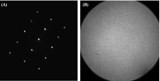
surface. The sample was then mounted onto the sample holder, loaded and transferred into the preparation chamber. There, the sample was heated to 150◦C for at least an hour for the desorption of gases from the sample surface. After cooling, the sample was cleaved in-situ with the transfer arm to reveal the <110> surface and then transferred into the main chamber for measurements. The cleaved surface was confirmed with both low energy electron diffraction (LEED) (Figure3.3A) and photoemission electron microscopy (PEEM) imaging (Figure 3.3B) to be pristine and free of microscopic ridges. A LEED pattern was measured both before and after the measurements to rule out significant surface changes over the course of measurements. All measurements were conducted at
Experimental setup & sample preparation 23
Figure 3.3: LEED & PEEM measurements of sample surface. (A) LEED pattern of the crystalline <110> surface measured at an electron energy of 32eV. (B) Photoemis- sion of the sample surface with 266nm probe. The field-of-view is set to be 75µm. The hair-like artifact near the lower left region is not a feature on the sample surface but an artifact on the detector system.
least an hour after cleavage due to the alignment of the electron microscope and as such the band bending process as described in [32] was not observed.
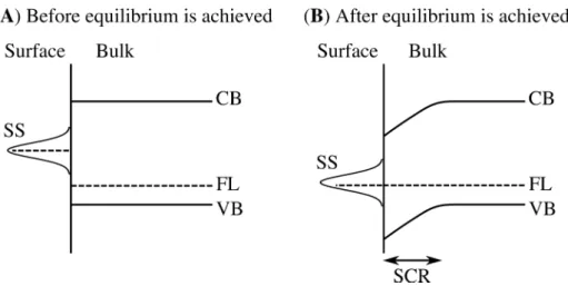
3.3.2 Existence of surface states
The origin and nature of the surface states of GaAs <110> has been extensively inves- tigated since 1970s [33, 34, 35, 36, 37, 38]. Although intrinsic surface states have been shown to be located outside of the band gap [39], mid-gap surface states have been known to occur due to cleavage defects [40] or gas adsorption on the sample surface [41]. In addition, by studying the surface band bending process of n- and p-type GaAs <110>
surfaces immediately after in-situ cleavage, Deng et al. has proposed that the relaxation of the surface lattice after cleavage could also lead to the creation of surface states [32].
Irregardless of the origin, the existence of the mid-gap surface states will cause the carrier distribution in the band structure to change, resulting in the formation of a surface space
Experimental setup & sample preparation 24
Figure 3.4: Surface bands bending in p-type GaAs. Band structures of p-type GaAs (A) before and (B) after equilibrium with the surface states is achieved. CB:
conduction band, FL: fermi level, VB: valence band, SS: surface states, SCR: space charge region.
charge region and the bending of the surface bands as illustrated in Figure 3.4.
3.3.3 Optical penetration depth of the pump and probe pulses
For the dopant concentration of1018cm−3, the depletion width of the space charge region, w, extends ∼32nm beneath the surface according to the following equation [42]:
w=
s2ε0εrΦb
qNd (3.1)
where ε0 is the vacuum permittivity, εr is the static relative permittivity, Φb is the band bending at the sample surface, q is the electron charge, andNdis the dopant concentration.
For the TR-PEEM measurement, both the pump and the probe beams are set to p- polarization with half wave plates placed right before the beams enter the main chamber of the microscope. The penetration depth of the 800nm pump is ∼700nm and that of the 266nm probe is ∼6nm [43,44]. The narrow penetration depth of the probe compared to the depletion width allows TR-PEEM the capability to resolve the vertical transport of the photocarriers within the space charge region. Due to the large penetration depth of the 800nm pump, the gradient of the photoexcited carriers across the depletion width is
Experimental setup & sample preparation 25
Figure 3.5: Schematic illustrating the extent of the optical penetration depths relative to the depletion width of the space charge region.
essentially constant.
3.3.4 Space charge effect
To demonstrate that the TR-PEEM measurements are not affected by any observable space charge effects due to the emitted photoelectrons, the photoemission spectrum for 266nm probe only is compared with the pump-probe photoemission spectra at the instant of photoexcitation i.e. at 0ps, for three different photoexcited carrier densities (Figure 3.6). The two peaks of the pump-probe spectra correspond to the surface states (lower energy) and the conduction band (higher energy) respectively. As the sample is hole- doped, very few electrons are photoemitted from the surface states at equilibrium. At 0ps, electrons are photoexcited from the valence band to both the surface states and the conduction band, resulting in a much higher photoemission signal from both states.
At the photoexcited carrier density of 8.4 x 1018cm−3, the integrated intensity shows approximately 100 times more photoelectrons detected than that with probe only (Figure
Experimental setup & sample preparation 26
Figure 3.6: Photoemission spectra showing no observable space charge effect.
(A) Comparison of probe only photoemission spectrum with the pump-probe spectra at 0ps for three different carrier densities. (B) Normalized photoemission spectra to highlight the absence of broadening of the spectra despite the large increase in the photoemitted electron density.
3.6A). Despite the large increase in the emitted photoelectrons, there are no observable broadening of the photoemission spectra (Figure 3.6B).
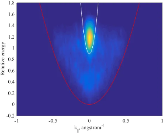
3.3.5 Confirmation of conduction band
The higher energy peak of the photoemission spectrum is confirmed to be the conduction band by matching the band dispersion in a time-resolved angle-resolved photoemission spectroscopy (TR-ARPES) measurement at 0ps (Figure3.7). The white and red quadratic lines each plot the energy-momentum dispersion relation i.e. E(k) = E0 + ¯h2m2k∗2 with the effective mass of 0.063m0 and m0 respectively. The white line that plots the band dispersion of the conduction band of GaAs matches well with the higher energy band in the TR-ARPES measurement indicating it to be the conduction band. As the energy separation between the two peaks in Figure 3.7 is ∼1eV and the band gap of GaAs is 1.42eV, the lower peak is attributed to be the surface states. The red line plots the instrument cut-off due to the energy of the probe photon.
Experimental setup & sample preparation 27
Figure 3.7: TR-ARPES of p-type GaAs <110> surface along the Γ-L direction at 0ps time delay
Experimental setup & sample preparation 28
3.3.6 Beam spot size measurement
Contrary to conventional pump-probe measurement, the pump spot in TR-PEEM is set to be much smaller than the probe spot to ensure homogeneous photoemission of the photoexcited electrons. The probe spot size is hence set to be much larger than the 75µm field-of-view (FoV). The FWHM of the probe spot is determined using the knife-edge method to be approximately 370µm in diameter. Due to the grazing angle of incidence, the pump beam is elongated in one axis forming an elliptical photoexcitation spot on the sample (Figure 3.8A). The shorter axis of the elliptical photoexcitation spot is set to be smaller than the FoV and can be accurately determined from the photoemission spatial profile. To measure the FWHM of the photoexcitation spot, we first established that the integrated photoemission intensity varies linearly with the pump power, as shown in Figure 3.8B. A line profile is then extracted along the short axis of the elliptical photoexcitation spot (as illustrated by the yellow line in Figure3.8A) and fitted with a Gaussian function showing a FWHM of ∼30µm (Figure 3.8C).
3.3.7 Temporal resolution of TR-PEEM
The temporal resolution of the TR-PEEM measurements is obtained from the rise time of the pump-probe signal measured at a 4µm x 4µm region at the center of the photoexcita- tion spot for a photoexcited carrier density of 1.1 x1019cm−3. The Gaussian fit of the rise time shows a FWHM of ∼280fs (Figure 3.9). The 800nm pump is measured before the microscope view port with an autocorrelator (F emtometerT M) to be ∼50fs. The cross correlation of the pump and probe Gaussian pulses is another Gaussian with a FWHM pulse width of q∆t2pump+ ∆t2probe where∆tpump and ∆tprobe are the FWHM of the pump and probe Gaussian pulses respectively [45]. With the equation, the 266nm probe pulse width is calculated to be ∼275fs. The broad 266nm pulse width is due to the laser pulse dispersion pre-compensation being optimized for maximum conversion efficiency of the harmonics and not for achieving the shortest pulse durations.
Experimental setup & sample preparation 29
Figure 3.8: Determination of photoexcitation spot size. (A) TR-PEEM image of the elliptical photoexcitation spot at 0ps. The field-of-view of the microscope is set to 75µm. (B) Integrated photoemission intensity of the field-of-view as a function of the pump power. The red line shows a linear fit of the data points. (C) Line profile extracted along the short axis of the elliptical photoexcitation spot for pump power of 30mW, as illustrated by the yellow line in (A). The red line shows a Gaussian fit of the profile with a FWHM of ∼30µm.
Experimental setup & sample preparation 30
Figure 3.9: Determination of TR-PEEM setup temporal resolution. Time- delayed photoemission intensity at a photoexcited carrier density of 1.1 x 1019cm−3. The temporal resolution of the TR-PEEM setup is estimated to be 280fs from the Gaussian fit (red solid line) of the rise time of the pump-probe signal (black data points).
Experimental setup & sample preparation 31
Figure 3.10: Determination of the photocarrier lifetime. An empirical tri- exponential fit of the pump-probe signal measured at a photoexcited carrier density of 1.1 x 1019cm−3. The fit shows a long-term decay time constant of∼460ps.
3.3.8 Determination of photocarrier lifetime
To have an idea of the timescale at which the photoexcited carriers in the GaAs sample relax back to its equilibrium state i.e. pre-pump state, we fit the pump-probe curve mea- sured at a photoexcited carrier density of 1.1 x1019cm−3with an empirical tri-exponential equation, as shown in Figure 3.10. The fit shows a long-term decay time constant of
∼460ps, denoting the timescale at which the photoexcited carriers relax back to its equi- librium state.
3.4 Chapter conclusion
The first part of this chapter described in detail the optical layout of the 3rd and 4th harmonic generation and the pump beam path. It then described the auxiliary chambers
Experimental setup & sample preparation 32 connected to the main chamber of the electron microscope and the coupling of the pump and probe beams into the main chamber for measurements. The second part of this chapter described the preparation method for obtaining a pristine <110> surface of the Zn-doped GaAs sample. It then went on to discuss the origin and nature of the surface states at GaAs <110> surface and how the creation of the surface states leads to the bending of the surface bands and the buildup of an intrinsic surface space charge field.
The width of the space charge region and the penetration depth of the ultrafast pulses are then calculated to showcase TR-PEEM capability to resolve the vertical transport of the photocarriers within the space charge region. The chapter then went on to compare the photoemission spectra of probe only with that of pump-probe measurements to verify that the TR-PEEM measurements are not affected by any observable space charge effect.
The two peaks of the photoemission spectra are confirmed to be the surface states and the conduction band via matching the band dispersion in the TR-ARPES measurement.
The chapter finished with the determination of the probe and the pump spot sizes as well as the temporal resolution of the TR-PEEM measurements to be ∼370µm, ∼30µm, and
∼280fs respectively. The next chapter will discuss the control of the vertical transport of electrons to the sample surface at early time delays.
Chapter 4
Controlling the vertical transport of photocarriers
4.1 Chapter overview
This chapter studies the control of vertical transport of photoexcited electrons to the sample surface at early time delays. Using TR-PEEM, the chapter first describes the visualization of inhomogeneous photocarrier dynamics on a homogeneous p-type GaAs sample where a depletion in the electron population is observed at the center of the photoexcitation spot while a gain in the electron population is observed near the FWHM boundaries. The chapter then goes on to discuss the two competing intensity-dependent processes i.e. the vertical transport of photocarriers due to the intrinsic surface field and the many body Auger processes that lead to the observed spatial variation in the photocarrier dynamics. With this understanding, the chapter then demonstrates that the intensity profile of the photoexcitation beam can be utilized to control these processes.
This is then followed by a discussion of how the inhomogeneous dynamics affects the electron distribution on the sample surface.
33
Controlling the vertical transport of photocarriers 34
4.2 Experimental method
As described in Chapter 3, the sample being studied is a p-type GaAs cleaved in-situ to expose a pristine <110> surface (Figure 3.3). A 1.55eV pump pulse is used to pho- toexcite the electrons above band gap and a 4.65eV probe pulse is used to photoemit the photoexcited electrons. The photoemitted electrons are then collected by PEEM to form a series of time-delayed images reflecting the distribution of the photoexcited electrons both in space and in time. The narrow penetration depth of the probe pulse compared to the width of the depletion region has allowed PEEM the capability to resolve the ver- tical transport of the electrons to the sample surface. To study the local photocarrier dynamics as a function of the intensity variation within the photoexcitation beam, the pump spot size is set to be much smaller than the probe spot size to ensure homogeneous photoemission. Due to the dissimilar intensity gradient along the two axes of the ellipti- cal photoexcitation spot (Figure 3.8A), the discussions in this chapter will focus on the variation in the local photocarrier dynamics along the short axis. Further details of the setup and the characterization of the sample are described in Chapter 3.
4.3 Inhomogeneity of physical processes within the full- width-half-maximum
Using TR-PEEM, the spatial distributions of the photoexcited electrons for three different photoexcited carrier densities are first imaged at a fixed time delay of +2.5ps (Figure 4.1A). The images are set to show the photocarrier dynamics within the FWHM of the short axis of the pump beam. Furthermore, to highlight the relative gain (red) or loss (blue) in the photoexcited electron density after the instant of photoexcitation, the images at +2.5ps delay are subtracted with their respective images at 0ps.
At low photoexcited carrier density (2.8 x1018cm−3), an increase in the photoexcited electron density is observed throughout the spot. The increase in the electron density af-
Controlling the vertical transport of photocarriers 35
Figure 4.1: Spatial inhomogeneity in the photocarrier dynamics within the FWHM.(A) Spatial distribution of the photoexcited electrons within the FWHM of the short axis of the elliptical photoexcitation spot at a fixed time-delay of +2.5ps after pho- toexcitation. The images are subtracted with their respective images at 0ps to highlight the relative gain (red) or loss (blue) of electrons after photoexcitation. The images are rotated so that the axes of the pump spot are parallel to the x-y coordinates. (B) Spatial distribution profile of the electrons extracted along the short axis (as indicated by the black double-headed arrow in (A)) for both 0ps and +2.5ps time delays.
Controlling the vertical transport of photocarriers 36 ter the instant of photoexcitation is a result of the vertical transport of the photoexcited electrons from the bulk to the sample surface due to the intrinsic surface space charge field (Figure 3.4). At high photoexcited carrier density (1.0 x1019cm−3), a general loss of the photoexcited electrons are observed throughout the spot. The depletion in the electron density is attributed to Auger recombination as discussed in the next section. In contrast to the general gain and loss of electrons observed at both the low and high photoexcited carrier densities, an intriguing spatial variation is observed at the intermediate photoex- cited carrier density (8.4 x 1018cm−3) – depletion of electrons is observed near the center of the photoexcited spot while an accumulation of electrons is observed further away from the center.
For quantitative comparison, the photoemission intensity profiles along the FWHM (as indicated by the double-headed arrow in Figure4.1A) for both 0ps and +2.5ps delays are extracted (Figure 4.1B). As demonstrated by the images, the photoemission intensity profiles show a general increase across the spot at low carrier density and a general decrease at high carrier density. At intermediate carrier density, the intensity profiles clearly show the contrasting photocarrier dynamics with a decrease in the photoemission intensity at the center of the FWHM and an increase near the FWHM boundaries. In addition to the intriguing spatial variation observed, a fine-tuning of the carrier density around the intermediate range further shows that the relative sizes of the two regions with contrasting dynamics can be finely controlled, as demonstrated in Figure 4.2.
4.4 Verification of vertical transport and Auger recom- bination
To verify that the vertical transport of the excited photocarriers and Auger recombination indeed lead to the observed gain and loss of electrons, the time-delayed photoemission in- tensity at a small 4µm x 4µm region at the center of the photoexcited spot is measured as a function of the photoexcited carrier densities (Figure 4.3A). The small measure-
Controlling the vertical transport of photocarriers 37
Figure 4.2: Controlling the relatives sizes of the two contrasting regions by fine-tuning the photoexcited carrier densities. The images are rotated with the axes of the elliptical photoexcitation spot parallel to the x-y coordinates for easy comparison.
ment region is chosen to ensure that the carrier dynamics is spatially averaged across an effectively constant photoexcitation intensity (Figure 4.3B–C).
For the low carrier densities, upon photoexcitation, the electrons drift towards the sample surface while the holes drift towards the bulk under the influence of the intrinsic surface field. This leads to an increase in the photoexcited electron density at the sample surface and hence the increase in the photoemission intensity (Figure 4.4A). The sepa- ration of the photoexcited electron-hole pair leads to the buildup of an opposite electric field that then partially screens the intrinsic surface field. As the carrier density increases, the partial screening of the intrinsic field becomes faster and more effective, resulting in reduced vertical transport of the photocarriers. A single exponential fit of the rise time of the pump-probe signals shows a decreasing trend from 3.5ps to 0.9ps (Table 4.1). At suf- ficiently high carrier density i.e. 9.8 x 1018cm−3 (Figure 4.3A), the intrinsic field becomes completely screened upon photoexcitation and no vertical transport of the photoexcited electrons is observed as evidenced by the lack of rise in the photoemission intensity. The signal instead decreases monotonously as the photocarriers decay and recombine over time. The observed screening dynamics as a function of the photoexcited carrier density (Figure 4.3A) agrees with previous literature [46].
In addition to the increasing partial screening of the intrinsic field, a rapid depletion
Controlling the vertical transport of photocarriers 38
Figure 4.3: Screening dynamics of the photocarriers as a function of the pho- toexcited carrier density. (A) Local time-delayed photoemission intensity as a function of the photoexcited carrier densities. (B) TR-PEEM image at 0ps indicating the 4µm x 4µm measurement region at the center of the photoexcitation spot. (C) Photoemission intensity profile along the short axis of the photoexcitation spot (as indicated by the yellow line in (B)) showing the effectively constant intensity across the 4µm spot.
Table 4.1: Single exponential fit of the rise time of time-delayed photoemission signals for low carrier densities.
Photoexcited carrier density
(cm−3) 2.8 x10¹⁷ 1.4 x10¹⁸ 2.8 x10¹⁸ 4.8 x10¹⁸
Rise time (ps) 3.5 2.6 1.4 0.9
![Figure 2.1: Schematic of Brüche’s 1 st PEEM system [13]](https://thumb-ap.123doks.com/thumbv2/123deta/6957953.2273250/23.892.148.748.156.417/figure-schematic-brüche-s-st-peem.webp)