PAPER
Special Section on Recent Trends of Microwave Systems and Their Fundamental TechnologiesLow-Loss Matching Network Design for Band-Switchable Multi-Band Power Amplifier
Atsushi FUKUDA†a), Takayuki FURUTA†,Members, Hiroshi OKAZAKI†, Shoichi NARAHASHI†,Senior Members,andToshio NOJIMA††,Fellow
SUMMARY This paper presents a novel design scheme for a band- switchable multi-band power amplifier (BS-MPA). A key point of the de- sign scheme is configuring multi-section reconfigurable matching networks (MR-MNs) optimally in terms of low loss matching in multiple frequency bands from 0.7 to 2.5 GHz. The MR-MN consists of several matching sec- tions, each of which has a matching block connected to a transmission line via a switch. Power dissipation at an actual on-state switch results in the insertion loss of the MR-MN and depends on how the impedance is trans- formed by the MR-MN. The proposed design scheme appropriately trans- forms the impedance of a high power transistor to configure a low loss MR-MN. Numerical analyses show quantitative improvement in the loss using the proposed scheme. A 9-band 3-stage BS-MPA is newly designed following the proposed scheme and fabricated on a multi-layer low temper- ature co-fired ceramic substrate for compactness. The BS-MPA achieves a gain of over 30 dB, an output power of greater than 33 dBm and a power added efficiency of over 40% at the supply voltage of 4 V in each operating band.
key words: power amplifier, reconfigurable, matching network, multi- band, switch
1. Introduction
There has been an increase in the number of frequency bands allocated to mobile communication services provided all over the world. Future mobile terminals will be expected to function seamlessly in various mobile communication systems. Numerous research activities have been focused on adaptive RF circuits that can function according to any specification [1], [2].
The Power amplifier (PA) is a key device in RF cir- cuits. The PA has a much greater impact on power dissi- pation than any other component in the RF circuits for mo- bile terminals. The PA must achieve a high level of oper- ating efficiency in order to maximize the battery life time and minimize the size and cost of the terminals even if the PA has to cover a wide band or multiple bands. Several ap- proaches have been developed for a multi-band PA [3]–[18].
A commonly used approach is “unit selection” [3], [4]. This scheme implements several PA units that operate efficiently in a single band or some adjacent bands. The circuit scale basically increases in proportion to the number of the PA
Manuscript received November 2, 2011.
Manuscript revised January 31, 2012.
†The authors are with NTT DOCOMO, INC., Yokosuka-shi, 239-8536 Japan.
††The author is with the Graduate School of Information Sci- ence and Technology, Hokkaido University, Sapporo-shi, 060- 08114 Japan.
a) E-mail: [email protected] DOI: 10.1587/transele.E95.C.1172
units. Another approach is the “broadband matching” [5], [6] or “multi-band matching” [7]–[9] that covers all or sev- eral operating bands employing specially-designed match- ing networks (MNs). The former, which has a flat frequency response over all operating bands, is inappropriate to config- ure a highly efficient PA when the upper and lower limits of the operating bands are far apart. The latter, which achieves optimum matching simultaneously in multiple bands, needs complex circuits to provide multi-band operation. More- over, designing multi-band MNs becomes difficult when the number of the operating bands increases. One practical ap- proach for the multi-band PA is to employ “reconfigurable MNs” [10]–[18] that change their frequency responses using variable devices. This type of structure represents a promis- ing solution because it has a reasonably sized circuit config- uration considering multiple band operation while providing adequate characteristics.
There have been reports on a 1-W class band recon- figurable PA employing micro-electro-mechanical systems (MEMS) Single-Pole-Single-Throw (SPST) switches [14]–
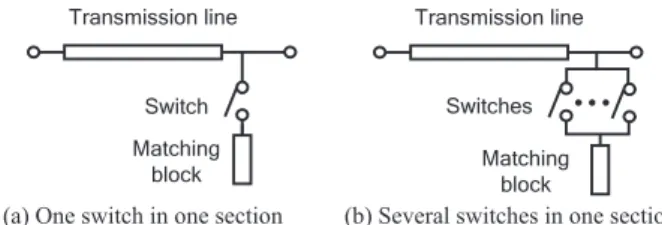
[16] as variable devices. The PA includes multi-section reconfigurable MNs (MR-MNs), which basically have one switch in one section as shown in Fig. 1(a), and exhibits performance levels close to those of a single-band PA in the 1, 1.5, 1.9 and 2.5-GHz bands [16]. The performance of the MEMS switch is close to that of an ideal switch with both a low insertion loss and a high isolation. How- ever, there are some issues that need to be addressed in ap- plying MEMS switches to mobile terminals, such as cost reduction, ensuring long-term reliability, and reducing the operating voltage. From a more practical view, applying semiconductor switches instead of MEMS switches is at- tractive to not only solve the above-mentioned issues but also facilitate a high level of integration for the PA. A band- switchable multi-band power amplifier (BS-MPA) employ- ing GaAs FET switches was fabricated and tested [17], [18].
Fig. 1 Configurations of one section in the MR-MN.
Copyright c2012 The Institute of Electronics, Information and Communication Engineers
The fabricated BS-MPA achieves an adequate gain and an output power of over several watts in 9 bands from 0.7 to 2.5 GHz allocated to mobile communications all over the world. However, since the equivalent resistance of the on- state FET switch is higher than that of the MEMS switch used in the previous studies, the power dissipation at the FET switch has a stronger influence on the performance of the PA than that from the MEMS switch. In [17] and [18], as shown in Fig. 1(b), some sections employed several switches instead of one switch in one section to reduce the current flowing through each on-state switch and the power dissipation at the FET switch. Reduction in the circuit size and cost of the configuration were required because many switches were implemented.
This paper presents a novel design scheme to config- ure the MR-MN with lower power dissipation at the on- state switch for low loss matching in individual bands. The scheme is based on the use of several sections that have one switch. This paper also describes numerical quantitative analyses of the power dissipations at the on-state switches based on the relational expressions between the impedance transformation and the current flowing through the switch.
These analysis results yield design parameters to achieve the low loss MR-MN and indicate improvement in the in- sertion loss by the MR-MN with the determined parameters compared to the conventional MR-MN. Following the de- sign parameters for the MR-MN, a 3-stage 9-band BS-MPA from 0.7 GHz to 2.5 GHz, i.e., 0.7, 0.8, 0.9, 1.5, 1.7, 1.8, 1.9, 2.3, and 2.5 GHz bands, is newly designed and fabricated on a multi-layer Low Temperature Co-fired Ceramic (LTCC) substrate. The experimental results of the BS-MPA show a gain exceeding 30 dB for each frequency band. The BS- MPA achieves an output power exceeding 33 dBm with the maximum power-added efficiency (PAE) of over 40% with a continuous wave (CW) test signal in the targeted 9 bands.
In addition, an output power of approximately 29 dBm un- der an Adjacent Channel Leakage Ratio (ACLR) of less than
−37 dBc is achieved with a W-CDMA test signal.
2. Band-Switchable Multi-Band PA
Figure 2 shows a block diagram of the 3-stage BS-MPA.
Since the output power of the first stage is at a low or medium level, broadband amplifiers with moderate effi- ciency can be applied to this stage. The second and third stages have a greater effect on the power consumption than the first stage. Therefore, the MNs for these two stages should be configured with the MR-MNs to achieve matching precisely.
2.1 Basic Configuration for MR-MN
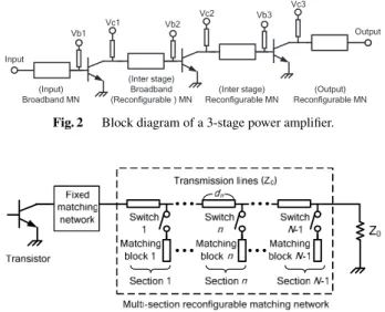
The MR-MNs proposed in [14] provide practical configu- rations for a reconfigurable MN. Figure 3 shows the basic configuration as the output MN for N-band operation. Here, Bn (1 ≤n ≤ N) is then-th band with the center frequency of fn. The fn is allocated in accordance with f1 >· · ·> fN.
Fig. 2 Block diagram of a 3-stage power amplifier.
Fig. 3 Basic configuration of a multi-section reconfigurable matching network applied to output matching network.
The whole MN includes a fixed MN and a MR-MN that consists of N−1 sections. One section has a shunt SPST switch connected to a transmission line (TL) for reconfigu- ration. In Fig. 3, the length of the TL,dn, and the reactance of matching blocknin the sectionnare designed to achieve matching inBn+1 on the assumption that switchn is in the on-state in single stub matching scheme [19]. The character- istic impedance of the TL is set to Z0 because the following sections prevent the impedances in the matched bands from being unmatched. The fixed MN is designed for matching inB1. The configurations of the fixed MN and each section basically have low-pass characteristics. The MR-MNs are reconfigured in accordance with the change in the operating band and provide an amplification device with the optimum impedance condition in each of multiple bands. Since no switches are inserted in series into the output signal paths, the configuration is expected to have less effect on the out- put power (Pout) and PAE. The same configuration can be applied to the input MN as well.
2.2 Low Loss Design for MR-MN
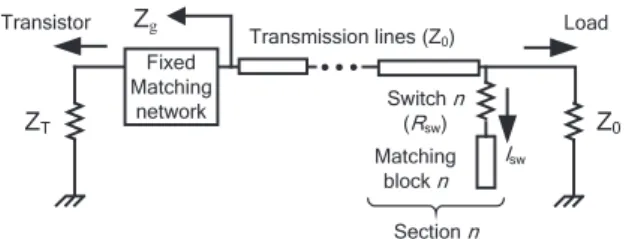
A simple equivalent circuit for an actual switch is described as a resistor for the low impedance in the on-state. Partic- ularly, the power dissipation at the on-state switch becomes potentially a serious issue due to decreases in the output power and operating efficiency. Figure 4 shows a circuit diagram for investigating the power dissipation at the on- state switch employed for matching in Bn+1 in Fig. 3. All switches except switchnare in the off-state. The off-state switches are not shown in Fig. 4 because their isolation is assumed to be infinite for the sake of simplicity. In Fig. 4, the TL length is the sum of the TLs between the first sec- tion and the section nin Fig. 3. In Fig. 4,ZT is the output impedance of the transistor. TermZgis the impedance where ZTis transformed by the fixed MN.
Power dissipation,Psw1, at the on-state switch, can be
Fig. 4 Circuit diagram for investigating power dissipation at on-state switch.
written as
Psw1=I2sw·Rsw, (1) whereRswis the equivalent resistance of the on-state switch andIswis the root mean square (RMS) RF current flowing through the switch. Here,Iswis given as
Isw= P
Z0
4Γg2
1−Γg2, (2)
where thePis the power delivered to the load,Z0, [15] and a mismatch loss byRswis not taken into account. The|Γg| is the magnitude of the complexΓg, which is the relation betweenZgandZ0, and defined as
Γg=Zg−Z0
Zg+Z0 =Γgejθg, (3) Then, the insertion loss of the MR-MN for matching inBn+1, Ln1, can be estimated as
Ln1=P/(P−Psw1)=1⎡⎢⎢⎢⎢⎢⎢⎣1−Rsw Z0
⎛⎜⎜⎜⎜⎜
⎜⎝ 4Γg2 1−Γg2
⎞⎟⎟⎟⎟⎟
⎟⎠
⎤⎥⎥⎥⎥⎥
⎥⎦. (4) From Eq. (2), Isw monotonically increases with respect to the increase in|Γg|. Then, Psw1 and Ln1 also increase as
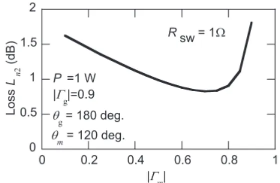
|Γg|increases as in Eqs. (1) and (4), respectively. For ex- ample, ifP=1 W,|Γg|=0.9 andRsw=1Ω,Ln1=1.81 dB is obtained from Eq. (4). On the other hand, the value for
|Γg|in each band is determined by ZT and the fixed MN.
Namely, the fixed MN is employed not only to configure the MN forB1 but also to reduce the power dissipation at the switches included in the MR-MN. Here,ZT is assumed to be constant in terms of frequency because theZT values of the actual transistor are approximately constant in the target bands. WhenZT is satisfied by|ΓT|=0.9 andθT=180 de- grees from Eq. (3), the calculated|Γg|,Ln1, and the improve- ment in the loss compared to that for the MR-MN without the fixed MN are indicated in Table 1. Here, 9 bands allo- cated for mobile communications are selected as the target bands for calculation. It is assumed that the TL and match- ing blocks are lossless. Table 1 shows that theLn1s in the higher bands are less than those in the lower bands because the|Γg|values in the higher bands become smaller than those in the lower bands due to the fixed MN. There is no loss from the switch for matching in the 2.5-GHz band. The improve- ments in the insertion loss are verified to be more than 1 dB
Table 1 Insertion loss and improvement effect for fixed MN.
Fig. 5 Circuit diagram for investigating the insertion loss due to two sections with on-state switches.
in the 1.5-GHz and higher bands. In general, the low loss characteristics of the MN in the high bands have additional advantages because it is more difficult to obtain an adequate gain or efficiency level depending on the performance of the transistor as the operating bands become higher.
For further improvement in the lower bands, the newly proposed design scheme employs several sections simulta- neously to decrease the power dissipation at the on-state switch. In this case, the insertion loss of the MR-MN is the sum of the power dissipation at each switch in the on- state. As the simplest case, Fig. 5 shows a circuit diagram for investigating the insertion loss of the MR-MN with two sections including the on-state switch, namely sectionmand sectionn. Sectionmis the newly added section or any sec- tion between section 1 and sectionn−1. The values of the currents flowing through the on-state switches are described asIswmandIswnin Fig. 5. In Fig. 5,Zgis transformed toZm
by sectionmand thenZmis transformed toZ0by sectionn.
The relation,Γm, betweenZ0andZmin Fig. 5 is defined as
Γm=Zm−Z0
Zm+Z0 =|Γm|ejθm, (5) where |Γm| and θm are the magnitude and phase angle of complexΓm, respectively. Then, from Eq. (5),
Gm=Y0
1− |Γm|2
1+2|Γm|cosθm+|Γm|2 (6) and
Bm=Y0 −2|Γm|sinθm
1+2|Γm|cosθm+|Γm|2, (7) whereYm=1/Zm=Gm+jBmandY0=1/Z0. On the other hand, in Fig. 5, the reactance,Y(dm)=G(dm)+jB(dm), at the distance of electrical length,dm, from the fixed MN on the TL is given as
G(dm)=Y0
1−Γg2 1+2Γgcos
2dm−θg
+Γg2 (8)
and
B(dm)=Y0
2Γgsin
2dm−θg
1+2Γgcos
2dm−θg
+Γg2. (9) SinceGm=G(dm) from Eqs. (6) and (8), we have
cos 2dm−θg
=|Γm|2−Γg2+|Γm|
1−Γg2 cosθm
Γg1−|Γm|2 .(10) From Eq. (10),dmcan be written as
dm= 1 2
cos−1α+θg
, (11)
where α is the right member of Eq. (10). When π/2 ≤ cos−1α ≤ π, the minimum dmdepends onθg and is given as
dm=
⎧⎪⎪⎪⎪⎪⎨
⎪⎪⎪⎪⎪
⎩
1 2
2π−cos−1(α)+θg
at−π<θg<−cos−1(α)
1 2
cos−1(α)+θg
at0≤θg≤cos−1(α)
1 2
−cos−1(α)+θg
atcos−1(α)<θg<π
. (12)
Then the susceptance of matching blockm,Bbm, can be writ- ten as
Bbm=Bm−B(dm). (13) At the matching condition, the RMS voltage, Vdm, at dm
from the fixed MN in Fig. 5 can be written as Vdm=
P/Gm. (14)
From Eqs. (13) and (14),Iswmis given as Iswm=|Bbm|
PZ0
1+2|Γm|cosθm+|Γm|2
1− |Γm|2 . (15) Here, when Eq. (15) is derived, the mismatch loss byRsw
is not taken into account. Figure 6 shows plots ofIswm as a function ofθm. Here, parameters ofP=1 W,|Γg|=0.9, andθg=180 degrees are selected as an example. According to Fig. 6,Iswmdepends onΓmtransformed fromΓg by sec- tionm. Meanwhile, Iswn can be calculated from Eq. (2) by substituting|Γm|instead of|Γg|after|Γm|is determined.
The total power dissipation,Psw2, due to two switches can be written as
Psw2=I2swm·Rsw+Iswn2 ·Rsw. (16) Then Ln2, which is the insertion loss of the MR-MN for matching inBn+1, can be expressed as
Ln2= 1
1−Rsw |Bbm|2Z0
1+2|Γm|cosθm+|Γm|2 1−|Γm|2
+Z10
4|Γm|2 1−|Γm|2
! (17)
Figure 7 shows plots ofLn2as a function ofθm. Parameters
Fig. 6 Root mean square (RMS) RF current flowing through the switch m.
Fig. 7 Estimated insertion loss of the MR-MN due to two sections with the on-state switches as a function ofθm.
Fig. 8 Estimated insertion loss of the MR-MN due to two sections with the on-state switches as a function of|Γm|.
of P=1 W,|Γg| =0.9, θg =180 degrees, and Rsw =1Ω are selected as an example. Loss Ln2 has the lowest value aroundθm=120 degrees at each|Γm|. Figure 8 shows plots of Ln2 as a function of |Γm| atθm =120 degrees and Ln2
has the lowest value around|Γm|=0.7. The low|Γm|value means a large impedance transformation betweenZgandZm
by sectionm, and as a result, Ln2 becomes large due to the largeIswm. On the other hand, a|Γm|value greater than 0.8 means a large impedance transformation betweenZmandZ0 by section n, andLn2 becomes large due to largeIswn. As shown in Figs. 7 and 8, Ln2 can be decreased below 1 dB, nevertheless,|Γg|=0.9 when the loss by one section,Ln1, is 1.81 dB, which is obtained from Eq. (4).
Table 2 shows a summary of the calculation results on the impedance transformations and the total improvement
Table 2 Insertion loss and total improvement for the MR-MN.
in the insertion loss due to the one or two sections. Here, the MR-MN due to the two sections is applied in the bands lower than 1.7-GHz band because of the insertion loss that exceeds 0.5 dB in the one section from Table 1. Improve- ment of more than 1 dB in the insertion loss is obtained by designing matching blockmso that it is satisfied by|Γm|= 0.7 andθm=120 degrees in the bands lower than 1.7-GHz band. In a practical design, any one section between the first section and the sectionn−1 can be applied as section mto achieve the condition regarding|Γm|andθminstead of adding a new section. It is also possible to employ more than two sections for a lower loss MR-MN using the exist- ing sections. This approach is very effective to reduce the circuit size and cost.
3. Design of MR-MN with FET Switches
To demonstrate the validity of the proposed design scheme, a 9-band PA was designed considering the characteristics of FET switches. The PA has 3 stages to provide the total gain of over 30 dB. Each stage is designed individually to match 50Ωbased on prior testing in each stage. The third stage is designed to achieve power matching based on non- linear simulations. In the design, the MR-MNs are adopted in not only the third stage but also the second stage. InGaP heterojunction bipolar transistors (HBTs) are used as am- plification devices. Nine bands, 0.7, 0.8, 0.9, 1.5, 1.7, 1.8, 1.9, 2.3, and 2.5 GHz, are selected as the applied or appli- cable bands for mobile communications all over the world.
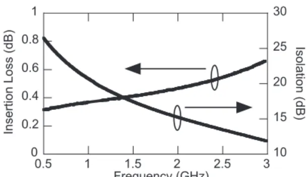
Figure 9 shows the measured insertion loss and isolation of the switch. Here, the effect of bonding wires and feed TL loss are included. The switch has an insertion loss of less than 0.7 dB and an isolation of greater than 13 dB over a frequency band below 3 GHz.
The power handling capability of the switch is also tested at 2.5 GHz as a representative frequency and shown in Fig. 10. The insertion loss and the isolation are almost constant at the input power of 15 to approximately 35 dBm.
Figure 11 shows the third-order intermodulation dis- tortion (IMD3) characteristics of the switch at various total power levels for 2-tone CW input signals (f1=2.500 GHz, f2=2.501 GHz). The third order input intercept point (IIP3) is estimated to be 67 dBm.
The power handling capability and distortion charac- teristics of the employed FET switch are thought to be satis-
Fig. 9 Measured insertion loss and isolation of the employed FET switch.
Fig. 10 Measured power handling capabilities of the employed FET switch.
Fig. 11 Measured third order intermodulation distortion (IMD3) characteristics of the employed FET switch.
factory to be applied to the MR-MN because the FET switch is a commercially available antenna switch for GSM appli- cation. However, the power dissipation at the FET switch, which is higher than that of the MEMS switch employed in previous reports, has a great impact on the output power and PAE degradations of the high power BS-MPA. In the de- sign of the 9-band PA, the configuration following the pro- posed design scheme is adopted in the MR-MN in the third stage where the power dissipation at the switches is out- side the allowable range. Figures 12(a), (b), and (c) show the schematics of the first, second, and third stages of the newly designed 9-band 3-stage BS-MPA, respectively. The first stage with broadband MNs operates in a wide frequency band. According to the basic configuration of the MR-MN shown in Figs. 3, 16 sections (8 for input and 8 for output MNs) in each stage are required for matching in the 9 bands.
Fig. 12 Schematics of the newly designed 9-band 3-stage BS-MPA.
However, 12 sections (8 for input and 4 for output MNs) are required for the second stage. Four sections suffice as the output MN because several sections cover plural bands. On the other hand, the third stage has 19 sections because three sections are added by the low loss design scheme described in Sect. 2.2. The total number of switches are 31.
4. Fabrication and Measurement
4.1 Fabrication
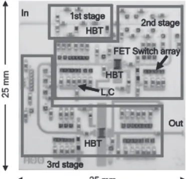
A prototype of the 9-band 3-stage BS-MPA was fabricated using LTCC technology. The dielectric constant and to- tal thickness of the substrate are 7.1 and 0.5 mm, respec- tively. RF signal lines, active devices (HBTs and switches), and discrete passive devices are implemented on the top layer. Because many bias lines for active devices can be implemented in the intermediate layers by employing the multi-layer substrate, compact integration of the BS-MPA can be achieved. A photograph of the fabricated BS-MPA is shown in Fig. 13. The size of the LTCC substrate is 25 mm×25 mm. A middle-power HBT with the emitter size of 1,248μm2 and 2 high-power HBTs with the emit- ter size of 7,488μm2 are deployed on the substrate for the first stage and for the second and third stages, respectively.
In Fig. 13, there are over 31 discrete switches and lumped elements because some of switches and elements are used for adjustment for matching in the experiment.
4.2 Measurement
Figure 14 shows the measured frequency responses of the fabricated BS-MPA at several switch states for the repre- sentative operation modes: (a) 0.7-GHz, (b) 0.8-GHz, (c) 0.9-GHz, (d) 1.5-GHz, (e) 1.7-GHz, (f) 1.8-GHz, (g) 1.9- GHz, (h) 2.3-GHz, and (i) 2.5-GHz modes. In Fig. 14, the 9-band BS-MPA achieves a gain of over 30 dB around each center frequency. Because of the influences of the bonding wires, the center frequencies in modes (h) and (i) shift lower by 50 MHz and 100 MHz, respectively. The collector supply
Fig. 13 Photograph of the fabricated 9-band 3-stage BS-MPA.
Fig. 14 Measured frequency responses of the fabricated BS-MPA.
voltage (Vc) and base supply voltage (Vb) are set to 3.5 V and 1.3 V (Class-A) for the first stage, 3.5 V and 1.28 V (Class- AB) for the second stage, and 4 V and 1.26 V (Class-B) for the third stage, respectively. The results show that the BS- MPA successfully changes its frequency response through the activation of FET switches. We also verified that it can achieve a level of performance close to that for band-free operation. No undesired oscillations are observed in any of the modes.
Figure 15 shows the Pout and PAE with the CW test at the center frequency of each mode for the (a) low band modes of 0.7/0.8/0.9 GHz, (b) middle band modes of 1.5/1.7/1.8/1.9 GHz, and (c) high band modes of 2.3/2.5 GHz. The HBTs are biased under the same condi- tions described above. According to Fig. 15, the gain ex- pansion in a high output power range is observed in each frequency.
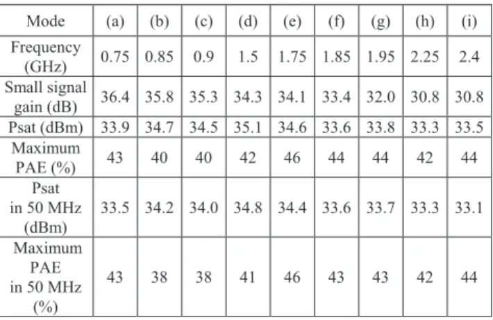
Table 3 shows a summary of the measurement results for the CW test. The gains in the low band modes are com- pressed by the first stage so that the difference in gain is small among operating bands. As a result, the difference in gain among the 9 bands is 5.6 dB. More specifically, the maximum gain of 36.4 dB in mode (a) and the minimum gain of 30.8 dB in mode (i) are achieved because of the in- trinsic gain of the HBTs. The saturation power level (Psat) exceeds 33 dBm in all bands. The maximum PAE value for each mode is over 40%. The Psat and maximum PAE at 50 MHz around the center frequency in each mode are also indicated to be over 33 dBm and 38%, respectively. It is verified that the PA operates with an adequate bandwidth in
Fig. 15 Measured gain and PAE versus Pout at the center frequency of each mode.
Table 3 Measurement results on CW test.
each mode.
Figure 16 shows the frequency responses for the maxi- mum Pout and PAE with W-CDMA (5-MHz adjacent chan-
Fig. 16 Measured frequency responses of Pout and PAE for W-CDMA test signal with ACLR<−37 dBc.
Table 4 Summary of Pout and PAE for W-CDMA test signal.
nel leakage power ratio (ACLR)<−37 dBc) for the (a) low band modes, (b) middle band modes, and (c) high band modes.
Table 4 shows a summary of the measurement results on the W-CDMA test with ACLR < −37 dBc test. The output power levels reach approximately 29 dBm in all the bands. The maximum PAE values in each mode are 21 to 33%. The PAE values are not so high. One of the reasons for the low PAE in the case of the W-CDMA test is that
Table 5 Performance comparison of multi-band reconfigurable PA.
the PAE values are deteriorated by the difference in ACLR levels between the upper and lower sides due to a memory effect.
Table 5 summarizes the performance of the state-of- the-art multi-band reconfigurable PA. A practical advantage of this work is that the proposed BS-MPA can operate in almost all the mobile communication bands with a moderate efficiency.
5. Discussion
This paper analyzes numerically the insertion loss of the MR-MN from the on-state switch. The numerical results show that it is preferable for the switch to have a low equiv- alent resistance in the on state such as the MEMS switch.
For example, Table 6 shows the calculated results of the loss of the MR-MN employing one section,Ln1, for matching in individual bands whenRsw =0.5Ω, which is achieved by the MEMS switch employed in previous studies [14]–[16].
However, a comparison of “Ln2” in Table 2 and “Ln1” in Table 6 shows that the proposed design scheme can de- crease the loss from the semiconductor switches to the same level as that from the MEMS switch. On the other hand, insufficient isolation of the switch may produce a mismatch loss in the MR-MN. It is also possible to suppress the mis- matching loss by designing the MR-MN by giving prelimi- nary consideration to the isolation. In general, it is difficult for semiconductor switches to have a low insertion loss in the on-state and a high isolation in the off-state at the same time. Therefore, the MR-MN should employ switches with as a low equivalent resistance as possible, while maintain- ing the minimum isolation, which depends on the design of the MR-MN. The relationship between the isolation of the switch and insertion loss of the MR-MN is shown in [15].
In addition, as a requirement for the switch applied to the MR-MN, the voltage limitation of the switch is an- other point to be considered. Since the positions where the off-state switches are connected depends on the operating bands, it is useful to consider the maximum voltage that can be distributed on the TL. Figure 17 shows a circuit diagram for investigating the voltage on the TL of the MR-MN.
The RMS voltage, V(dv), at distance of electrical length,dv, from the fixed MN on the TL can be written as
V(dv)=
PZ0
1+2Γgcos 2dv−θg
+Γg2 1−Γg2 . (18)
Table 6 Calculation results on loss from MEMS switch.
Fig. 17 Circuit diagram for investigating the voltage on the transmission line.
Fig. 18 Maximum root mean square RF voltage on the transmission line.
Then the maximumV(dv)maxon the TL depends on|Γg|and is given as
V(dv)max=
⎧⎪⎪⎪⎪⎪⎪⎪⎪
⎪⎪⎨⎪⎪⎪⎪⎪
⎪⎪⎪⎪⎪
⎩
PZ0
1+2|Γg|cos(2dv−θg)+|Γg|2
1−|Γg|2 at cos
θg
+Γg≥0
√PZ0 at cos
θg
+Γg≥0
. (19)
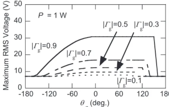
Figure 18 shows plots ofV(dv)max as a function ofθg. Here, parametersP=1 W is selected as an example. The fixed MN should be designed considering the voltage lim- itation of the switch because V(dv)max becomes large de- pending on |Γg|, i.e., V(dv)max is 30 V if|Γg| =0.9 andθg
=0 degrees, as shown in Fig. 18.
6. Conclusion
This paper presented a novel design scheme for a highly effi- cient BS-MPA employing the MR-MN. The design scheme focuses on reducing the power dissipation at the on-state switch in the MR-MN. The proposed scheme employs sev- eral sections that match the impedance in stages to mini- mize the power dissipation. The calculation results through derived equations on the loss of the MR-MN indicate quan- titative improvement by applying the proposed scheme. Ac- cording to a design example under practical conditions,
the impedance transformation by the proposed scheme im- proves the insertion loss by more than 1 dB. The fabricated LTCC 9-band BS-MPA including newly designed MR-MNs successfully switches its operating band from 0.7 to 2.4 GHz through activation of the switches. A satisfactory output power level and PAE value in each band are also obtained in the CW test although the PAE at the input of a W-CDMA signal needs to be improved. The measurement results con- firm that the proposed design scheme achieves low loss MR- MN for a highly efficient BS-MPA. The BS-MPA will con- tribute greatly to achieving a compact multi-band mobile terminal. Future issues to be addressed are evaluating the loss of the MR-MN experimentally, achieving a BS-MPA with a more practical circuit size, and improving the PAE observed in the W-CDMA signal test after investigating in detail the distortion. As a practical BS-MPA, a compact- sized BS-MPA is reported in [20] followed by the proposed scheme.
References
[1] G. Hueber and R.B. Staszewski, Multi-mode/Multi-band RF transceivers for wireless communications: Advanced techniques, Architectures, and Trends, Wiley-IEEE Press, 2011.
[2] A. Van Bezooijien, R. Mahmoudi, and A. Van Roermund, Adaptive RF front-ends for hand-held applications, Springer-Verlag, 2011.
[3] S. Zhang, J. Madic, P. Bretchko, J. Mokoro, R. Shumovich, and R. McMorrow, “A novel power-amplifier module for quad-band wireless handset applications,” IEEE Trans. Microw. Theory Tech., vol.51, no.11, pp.2203–2210, Nov. 2003.
[4] W. Bakalski, B. Sogl, M. Zannoth, M. Asam, B. Kapfelsperger, J.
Berkner, B. Eisener, W. Thomann, S. Marcon, W. Osterreicher, E.
Napieralska, E. Rampf, A.L. Scholtz, and B-U. Klepser, “A quad- band GSM/EDGE-Compliant SiGe-bipolar power amplifier,” IEEE J. Solid-State Circuits, vol.43, no.9, pp.1920–1930, Sept. 2008.
[5] A. Sayed and G. Boeck, “Two-stage ultrawide-band 5-W power am- plifier using SiC MESFET,” IEEE Trans. Microw. Theory Tech., vol.53, no.7, pp.2441–2449, July 2005.
[6] I.J. Bahl, “0.7–2.7-GHz 12-W power-amplifier MMIC developed us- ing MLP technology,” IEEE Trans. Microw. Theory Tech., vol.55, no.2, pp.222–229, Feb. 2007.
[7] S.H. Ji, C. Cho, J.W. Lee, and J. Kim, “Concurrent dual-band class- E power amplifier using composite right/left-handed transmission lines,” IEEE Trans. Microw. Theory Tech., vol.55, no.6, pp.1341–
1347, June 2007.
[8] P. Colantonio, F. Giannini, R. Giofre, and L. Piazzon, “A design technique for concurrent dual-band harmonic tuned power ampli- fier,” IEEE Trans. Microw. Theory Tech., vol.56, no.11, pp.2535–
2555, Nov. 2008.
[9] D.E. Dawson, “Closed-form solutions for the design of optimum matching networks,” IEEE Trans. Microw. Theory Tech., vol.57, no.1, pp.121–129, Jan. 2009.
[10] Y. Lu, D. Peroulis, S. Mohammadi, and L.P.B. Katehi, “A MEMS reconfigurable matching network for a class AB amplifier,” IEEE Microw. Wireless Compon. Lett., vol.13, no.10, pp.437–439, Oct.
2003.
[11] H. Zhang, H. Gao, and G-P. Li, “Broad-band power amplifier with a novel tunable output matching network,” IEEE Trans. Microw. The- ory Tech., vol.53, no.11, pp.3606–3614, Nov. 2005.
[12] W.C.E. Neo, Y. Lin, X. Liu, L.C. N. de Vreede, L.E. Larson, M.
Spirito, M.J. Pelk, K. Buisman, A. Akhnoukh, A. de Graauw, and L.K. Nanver, “Adaptive multi-band multi-mode power amplifier us- ing integrated varactor-based tunable matching networks,” IEEE J.
Solid-State Circuits, vol.41, no.9, pp.2166–2176, Sept. 2006.
[13] H.M. Nemati, J. Grahn, and C. Fager, “Band-reconfigurable LD- MOS power amplifier,” Proc. 40th European Microwave Confer- ence, pp.978–981, Paris, 2010.
[14] A. Fukuda, H. Okazaki, T. Hirota, and Y. Yamao, “Novel 900 MHz/1.9 GHz dual-mode power amplifier employing MEMS switches for optimum matching,” IEEE Microw. Wireless Compon.
Lett., vol.14, no.3, pp.121–123, March 2004.
[15] A. Fukuda, H. Okazaki, T. Hirota, and Y. Yamao, “Novel band-reconfigurable high efficiency power amplifier employing RF-MEMS switches,” IEICE Trans. Electron., vol.E88-C, no.11, pp.2141–2149, Nov. 2005.
[16] A. Fukuda, H. Okazaki, and S. Narahashi, “Highly efficient multi- band power amplifier employing reconfigurable matching and bi- asing networks,” IEICE Trans. Electron., vol.E93-C, no.7, pp.949–
957, July 2010.
[17] A. Fukuda, K. Kawai, T. Furuta, H. Okazaki, S. Oka, S. Narahashi, and A. Murase, “A high power and highly efficient multi-band power amplifier for mobile terminals,” Proc. Radio and Wireless Sympo- sium (RWS), pp.45–48, New Orleans, 2010.
[18] T. Furuta, A. Fukuda, K. Kawai, H. Okazaki, and S. Narahashi,
“Multi-band power amplifier on an LTCC Substrate,” IEEE Topi- cal Symposium on Power Amplifiers for Wireless Communications (PAS), Sept. 2010.
[19] D.M. Pozar, “Impedance matching and tuning,” in Microwave Engi- neering, Chapter 5, pp.251–299, John Wiley & Sons, 1998.
[20] T. Furuta, A. Fukuda, K. Kawai, H. Okazaki, and S. Narahashi,
“Compact 1.5 GHz to 2.5 GHz multi-band multi-mode power am- plifier,” IEICE ELEX, June 2011.
Atsushi Fukuda received the B.E. and M.E.
degrees in electrical engineering from Tokyo University of Science, Tokyo, Japan, in 1997 and 1999, respectively. In 1999, he joined NTT DOCOMO, INC., where he is involved in re- search on RF circuits and development on base station equipments for mobile communication systems. He is a member of the IEEE.
Takayuki Furuta received the B.E.
and M.E. degrees in electric engineering from Hokkaido University, Sapporo, Japan, in 2002 and 2004, respectively. In 2004, he joined NTT DoCoMo wireless laboratories, where he is involved in research on RF and microwave circuits for mobile communication systems.
Mr. Furuta was the recipient of the 2010 Young Researcher’s Award presented by IEICE.
Hiroshi Okazaki received the B.E. and M.E. degrees from Osaka University, Osaka, Japan, in 1988 and 1990, respectively, and Dr. Eng. degree from Tokyo Institute of Tech- nology, Tokyo, Japan, in 2011. In 1990, he joined NTT Radio Communication Laborato- ries, Kanagawa, Japan, where he was engaged in research on microwave circuits and equipments for communication systems. During 2001–
2003, he was with NTT Electronics Corpora- tion, Tokyo, Japan, where he was engaged in development of ultra-high-speed devices for photonic communication sys- tems. Since 2003, he has been with NTT DOCOMO, INC., where he is involved in research on RF circuits for mobile communication systems.
Dr. Okazaki was the recipient of the 1997 Young Engineer Award pre- sented by IEICE and the 1998 Japan Microwave Prize at 1998 Asia Pacific Microwave Conference. He is a senior member of the IEEE.
Shoichi Narahashi received the B.E.
and M.E. degrees from Kumamoto University, Kumamoto, Japan, in 1986 and 1988, respec- tively, and the Ph.D. degree from Hokkaido University, Sapporo, Japan, in 2008. In 1988, he joined Nippon Telegraph and Telephone (NTT) Radio Communication Systems Labora- tories where he was engaged in research and de- velopment on base station equipment for digi- tal mobile communications. Since 1992, he has been with NTT DOCOMO, INC. He is currently an Executive Research Engineer of Research Laboratories with the mission of investigating RF circuits for mobile communications. He is a member of the IEEE and the Society of Instrument and Control Engineers (SICE).
Toshio Nojima received his M.E. and Ph.D. degrees in electronic engineering from Hokkaido University, Sapporo, Japan. From 1974 to 1992, he was with Nippon Telegraph and Telephone (NTT) Communications Labo- ratories, where he was engaged in the research and development of high capacity microwave re- lay systems (SSB-AM and 256QAM systems).
From 1992 to 2001, he was with NTT DoCoMo, Inc., where he was a Senior Executive Research Engineer and pursued researches on the mobile communication RF technologies including EMC. Currently, he is a Profes- sor of the graduate school of Information Science and Technology, Hok- kaido University. He is a member of the IEEE and the Bioelectromagnetics Society (BEMS).