JAIST Repository
https://dspace.jaist.ac.jp/Title
Achieving high efficiency and stability in inverted organic solar cells fabricated by laminated gold leaf as top electrodes
Author(s) Razali, Nur Tahirah; Osaka, Itaru; Takimiya, Kazuo; Vohra, Varun; Murata, Hideyuki
Citation Applied Physics Express, 7(11): 111602-1-111602-4 Issue Date 2014-11-07
Type Journal Article
Text version author
URL http://hdl.handle.net/10119/12863
Rights
This is the author's version of the work. It is posted here by permission of The Japan Society of Applied Physics. Copyright (C) 2014 The Japan Society of Applied Physics. Nur Tahirah Razali, Itaru Osaka, Kazuo Takimiya, Varun Vohra, and Hideyuki Murata, Applied Physics Express, 7(11), 2014, 111602.
http://dx.doi.org/10.7567/APEX.7.111602 Description
Achieving High Efficiency and Stability in Inverted Organic Solar Cells
Fabricated by Laminated Gold Leaf as Top Electrodes
Nur Tahirah Razali,1,3) Itaru Osaka,2) Kazuo Takimiya,2) Varun Vohra,1,a) and Hideyuki Murata1
1
School of Materials Science, Japan Advanced Institute of Science and Technology, Nomi, Ishikawa 923-1211, Japan
2
Center for Emergent Matter Science, RIKEN, 2-1 Hirosawa, Wako, Saitama 351-0106, Japan
3
Faculty of Engineering, Universiti Malaysia Sarawak, 94300 Kota Samarahan, Sarawak, Malaysia
E-mail: [email protected].
We investigated inverted bulk heterojunction solar cells fabricated with gold (Au) leaf as laminated top electrodes. We demonstrate that the Au leaf can be successfully transferred from a supporting polyethylene terephthalate (PET) substrate to the surface of poly(3,4-ethylenedioxythiophene) poly(styrenesulfonate) (PEDOT:PSS) due to sufficiently higher work of adhesion with PEDOT:PSS compared to PET. By optimizing the lamination conditions, the contact between the Au leaf and the PEDOT:PSS becomes homogeneous and the power conversion efficiency (PCE) improves. Using Naphtho[1,2-c:5,6-c']bis[1,2,5]thiadiazole based polymer as the p-type semiconductor, the PCE reaches 5.07%. The laminated devices exhibit excellent stability comparable to that of the evaporated devices. _____________________________
a)
Present address: Department of Engineering Science, The University of Electro-Communications, 1-5-1 Chofugaoka, Chofu, 182-8585 Tokyo, Japan
In the solar cells industry, inorganic devices are still leading in terms of power conversion efficiency (PCE) when compared to the organic solar cells (OSCs). However, due to the high manufacturing cost of inorganic devices, more researchers and industries are shifting towards OSCs which could overcome this issue by using solution processes.1-2) For instance, OSCs offers high throughput manufacturing based on a continuous roll-to-roll process, where the costly metal electrode deposition process could be replaced by other processes such as a lamination.3-6) Previously, a study of the metal electrodes lamination for OSCs was conducted in regular bulk heterojunction (BHJ) solar cells with aluminum (Al) and calcium (Ca) as top electrodes. However, the device performances were rather low as these metal electrodes are easily oxidized.7) Recently, air stable inverted devices were successfully fabricated through lamination,2, 8-12) using more stable metals such as gold (Au) as the top electrode11) with the highest PCE reported reaching 4.0%.8) Furthermore, unlike vacuum evaporation, which induces penetration of metal particles inside the underlying layers, damages to the active layer are avoided by using the metal electrodes lamination.13) In literature, two types of lamination approaches have been reported. The first approach relies on evaporation of the metal on other substrates followed by lamination, where the purpose of the lamination is to prevent damage to the active layer through direct evaporation.11-12) While this method still requires vacuum evaporation of metal, the second method completely eliminates it by depositing the electrode on a substrate using a solution process, which will then be laminated.2,10) However, such solution processed electrodes require elaborated chemistry to prepare a stable metal dispersion and a careful control over solution deposition conditions to obtain continuous metallic films.
Recent studies show that laminated devices can be realized by improving adhesion at the interface between two substrates by controlling the surface free energy through UV light irradiation14-15), O2-plasma treatment16) or by adding surfactants into
poly(3,4-ethylenedioxythiophene) poly(styrenesulfonate) (PEDOT:PSS).10-12,17) Despite the improvements of the PCE in laminated devices through process engineering, there is a lack of quantitative explanations to describe how one can control the transfer and the adhesion of the laminated electrode. A study using double cantilever beam test is used to quantify the fracture energy of the interlayer adhesion between a laminated electrode and an organic layer.18) However, this method can only be performed after completing the devices and therefore, does not allow material selection by estimating the adhesion properties of the laminated metal electrodes prior to the device fabrication.
In this study, we demonstrate that efficient and stable inverted BHJ devices using laminated Au leaf as electrode. The key to successfully transferring the Au leaf from its supporting polyethylene terephthalate (PET) substrate to the PEDOT:PSS surface is to obtain sufficiently higher work of adhesion between Au leaf and PEDOT:PSS than that of the Au leaf and PET. The work of adhesion is the work required to separate two bodies that are in contact. Increasing the lamination temperature results in a better contact coverage between Au leaf and PEDOT:PSS which increases the device performances. Results obtained with laminated Au leaf devices based on poly(3-hexylthiophene) (P3HT):[6,6]-phenyl-C61-butyric acid methyl ester (PC61BM) blend as the active layer show slightly lower efficiency but are comparable in terms of device stability, to the evaporated Au electrode reference devices. Using a Naphtho[1,2-c:5,6-c']bis[1,2,5]thiadiazole based p-type polymer (PNTz4T):[6,6]-phenyl-C71-butyric acid methyl ester (PC71BM) blend as the active layer, our laminated devices reach the average PCE of 5.07%.
The fabrication method of metal leaves is based on rolling and pounding. The process starts with rolling the metal into a thin strip, followed by beating the strip into 50-100 µm thick foil. This thin foil is then cut and placed between layers of acetate pieces and pounded
until the area increases 4 times. It is then quartered, sandwiched and pounded. These processes are repeated until the metal sheet thickness is reduced to around 100 nm.19)
As shown in Fig. 1(a), the devices are prepared with the following architecture: glass substrate/indium tin oxide (ITO)/titanium oxide (TiOx)/active layer/PEDOT:PSS with Triton X-100/Au. TiOx films were obtained by the chemical bath preparation technique.20) The P3HT:PC61BM solution (25:20 mg/ml in chlorobenzene) or PNTz4T:PC71BM solution (6:12 mg/ml in dichlorobenzene) was spin coated on top of the TiOx film as the active layers. PEDOT: PSS was then spin-coated using Triton X-100 as an additive, which is a non-ionic surfactant that allows for PEDOT:PSS to wet and form a continuous layer on top of the organic active layers. For control devices, the electrodes were deposited by vacuum evaporation at the pressure of 9×10⁻⁷ Torr. The device area was defined by the overlapped area between the ITO and the Au, which was 0.02 or 0.04 cm2 for evaporated devices and 0.1 cm2 for laminated devices. For laminated devices, we used a commercially available pure Au leaf (> 99.95%). The Au leaf supported by PET is placed on top of the PEDOT:PSS film and rolled through the lamination machine at a roller speed of 1.5 rpm, a temperature between 100 ˚C to 150 ˚C and with an applied pressure of 0.1 MPa in air (Fig. 1(b)). The time required to form the Au electrodes by the lamination was only 3 min. After metal electrode deposition, both evaporated and laminated P3HT:PC61BM devices were post-annealed at 150 ˚C for 5 min and subsequently at 70 ˚C for 30 min. In the case of PNTz4T:PC71BM devices, the lamination of Au leaf was carried out at 130 ˚C and both laminated and evaporated PNTz4T:PC71BM devices were not subject to the post-annealing because we observed the degradation of the device performance at higher lamination temperature >130 ˚C or by post-annealing after electrode deposition. The PV characteristics of the devices were measured using a sourcemeter (Keithley 2400) and a solar simulator (AM 1.5G, 100 mW/cm2) at room temperature.
The free standing Au leaf (100 nm) is fragile and show brittle fracture properties.19) Therefore, supporting substrates, such as PET and polyvinylidene chloride (PVdC), are necessary as they provide a means to manipulate mechanically robust flexible substrate/Au leaf bilayer sheets. To obtain a complete transfer, the adhesion between Au/PEDOT:PSS should be stronger than that of the Au/PET or Au/PVdC. To quantify the difference in the adhesion at these two interfaces, we calculate their work of adhesion (W). For instance, if W between film x and substrate y (Wx/y) is larger than the Wbetween film x and substrate z (Wx/z)
then film x will attach to the substrate y instead of substrate z. These calculations can be completed prior to the device fabrication to select the appropriate materials as supporting substrate.
To calculate W, we first need to find the total surface free energy for each of the solid (film and substrates) surfaces (s) which can be obtained through the contact angle ()
measurement. The contact angle measurement is conducted on the various solid surfaces with a selection of measuring liquids (chlorobenzene, chloroform, dichloromethane and benzaldehyde) using an optical tensiometer (Attension Theta, Biolin Scientific). Applying Owens and Wendt equation (eq. 1)21) to the four solvents system, we extrapolate the s as described below:
d s d l p l p s d l l
2
cos
1
. (1)Equation 1 correlates the various components of the surface free energy
with the between the solid surface and the measuring liquid. The polar and dispersive components ofl
correspond to the surface free energies of the solid and measuring liquid, respectively. The values for lp and ld of the four solvents were taken from the measuring equipment database and correspond to the values found in literature.
By plotting the graph of
d l l 2 cos 1 versus d l p l , sd and sp values can be
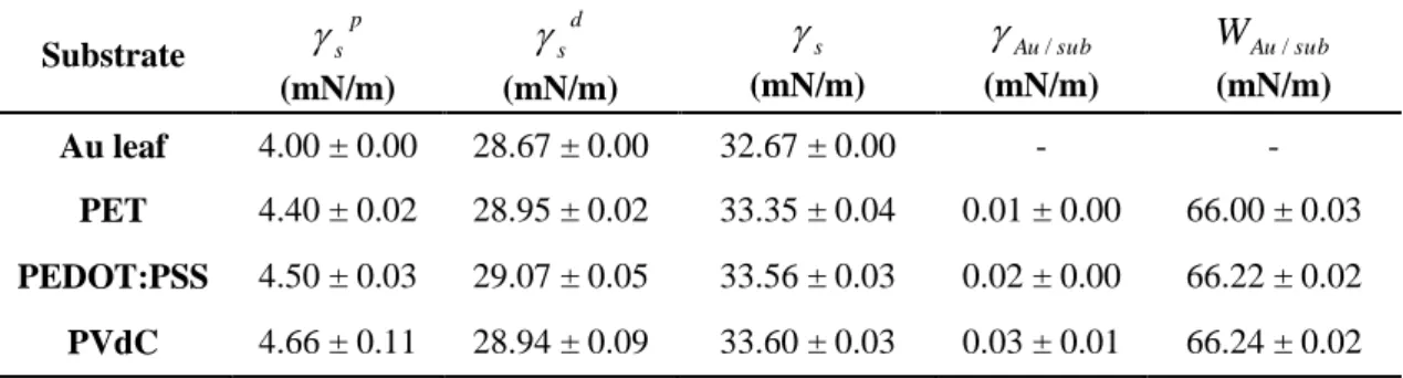
extracted, and then the s can be calculated as the sum of these values. We found that the s of Au leaf, PEDOT:PSS, PVdC and PET substrate are, 32.67 ± 0.00 mN/m, 33.56 ± 0.03 mN/m, 33.60 ± 0.03 mN/m and 33.35 ± 0.04 mN/m, respectively. Detailed values ofsd, sp and s for Au leaf, PEDOT:PSS, PVdC and PET substrate can be found in Table I.
Once the values for the s of all films and substrates are obtained, the interfacial energy values between Au leaf with PEDOT:PSS, PVdC or PET substrates (sub), (Au/ sub) can be calculated through eq. 2 (Table I). Finally, using eq. 3, we obtained the W between Au leaf with PEDOT:PSS, PVdC and PET substrates (WAu/ sub) . We found that the W of
Au/PEDOT:PSS (66.22 ± 0.02 mN/m) is slightly higher than the W of Au/PET (66.00 ± 0.03 mN/m) and similar to the W of Au/PVdC (66.24 ± 0.02 mN/m). Thus, the difference of W adhesion between Au/PEDOT:PSS and Au/PET; and between Au/PEDOT:PSS and Au/PVdC are 0.22 mN/m and 0.02 mN/m, respectively. From the experimental results, we found that the Au leaf on the PET substrate is successfully transferred to the PEDOT:PSS surface. However, when we tried to transfer the Au leaf from PVdC to the PEDOT:PSS surface, the Au leaf breaks from the PVdC surface and partially transferred to the PEDOT:PSS surface. These results show that the differences of W more than 0.22 mN/m are sufficient to transfer the Au leaf from one substrate to another. On the other hand, the unsuccessful transfer of the Au leaf on PVdC substrate to the PEDOT:PSS surface can be explained by the insufficient difference of W between Au/PVdC and Au/PEDOT:PSS.
To further confirm that the theoretical calculations match the experimental results, we attempted to transfer the Au leaf from the PET substrate to the PVdC substrate (difference of
W of 0.24 mN/m), and found that the Au leaf is successfully transferred from the PET
substrate to the PVdC substrate. Based on these results, we conclude that the W is a useful parameter to choose the suitable supporting materials for successful transfer during lamination.
p
sub p Au d sub d Au sub Au sub Au
/
2
2
, (2) sub Au sub Au sub AuW
/
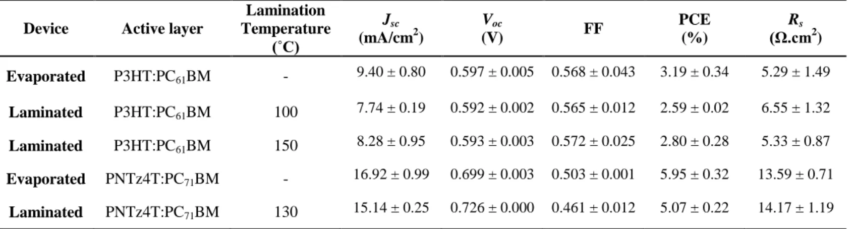
/ . (3)The current density - voltage (J-V) curves of evaporated Au metal and laminated Au leaf devices with P3HT:PC61BM as the active layer are shown in Fig. 1(c) and their PV parameters are summarized in Table II, where the data obtained from 4 cells are averaged. The evaporated Au devices exhibit 9.40 ± 0.80 mA/cm2 of Jsc, 0.597 ± 0.005 V of Voc, 0.568
± 0.043 of FF, 5.29 ± 1.49 Ω.cm2 of Rs and 3.19 ± 0.34% of PCE. For the Au leaf devices
laminated at 100 ˚C, the Jsc, Voc, FF, Rs and PCE are 7.74 ± 0.19 mA/cm2, 0.592 ± 0.002 V,
0.565 ± 0.012, 6.55 ± 1.32 Ω.cm2 and 2.59 ± 0.02% respectively. The Jsc, FF and Rs are
related to the contact quality at the top electrode and to charge collection efficiency.22-23) These device parameters in laminated devices suggest that their lower performances may be related to the contact condition at the Au/PEDOT:PSS interface. The images of the top electrode surfaces were taken using an optical microscope (Fig. 2). Evaporated Au electrode exhibit complete coverage of the Au on the surface of PEDOT:PSS (Fig. 2(a)) while laminated Au electrode shows some wrinkles as a result of inhomogeneous coverage between Au leaf/PEDOT:PSS interface (Fig. 2(c)). These wrinkles are already formed when the Au
leaf is deposited on the supporting PET substrate (Fig. 2(b)) prior to the lamination process. By increasing the lamination temperature from 100 ˚C to 150 ˚C, the electrode shows better coverage of Au leaf on the PEDOT:PSS (Fig. 2(d)). At higher temperature, the modulus of elasticity of metal will decrease and the softer Au leaf thus spreads more smoothly on the PEDOT:PSS surface during lamination.24) As a result, the parameters of the devices laminated at 150 ˚C increased to 8.28 ± 0.95 mA/cm2 of Jsc, 0.593 ± 0.003 V of Voc, 0.572 ±
0.025 of FF, 5.33 ± 0.87 Ω.cm2 of Rs and 2.80 ± 0.28% of PCE.
Using Au leaf combined with lamination process presents a major advantage over the evaporation process as it reduces the production cost by removing the losses of materials on the evaporation chamber walls.19) The time required to form the electrodes can be shortened drastically as it takes only 3 min to deposit metal leaves electrodes.
We further investigate P3HT:PC61BM stability properties and find that both unencapsulated laminated and evaporated Au devices demonstrate similar stability behavior under constant light irradiation up to 15 h. We observe a light soaking effect (LSE) during the first 5 min measurement (Fig. 3). This LSE results from the filling of the TiOx electron traps when the devices are exposed to light irradiation thus enhancing the charge collection properties of TiOx layer.25-26) After the initial increase, the PCE of the devices remain stable up to 3 h. Both devices show good stability where the decreases in PCE are only of 10% and 13% for evaporated and laminated devices, respectively (Fig. 3). This similar stability trend indicates that the adhesion between Au leaf/PEDOT:PSS is strong and shows no sign of delamination, which confirms that contact quality of the laminated Au electrode is comparable to that of the evaporated Au electrode. At the same time, PEDOT:PSS layer acts as a barrier to prevent the oxygen from entering the active layer prior to top electrode deposition.27)
With the emergence of high performance p-type polymers, the device performance of OSCs is constantly increasing. We fabricated evaporated and laminated devices using a new highly efficient polymer: PNTz4T.28) Figure 1(c) shows the J-V curves of both evaporated and laminated devices and their parameters are summarized in Table II, where the data obtained from 2 cells are averaged. Laminated devices exhibit slightly lower PCE (5.07 ± 0.22%) compared with that of the evaporated device (5.95 ± 0.32%). Although a reduction in the average PCE was observed, it corresponds to the highest reported efficiency for laminated devices.8, 16, 17)
In conclusion, we fabricate efficient and stable inverted BHJ solar cells using Au leaf as laminated top electrode, which completely removes the use of the costly vacuum evaporation process. We show that the Au leaf is successfully transferred from the supporting PET substrate to the PEDOT:PSS surface due to the sufficient difference in W values between Au/PEDOT:PSS and Au/PET. By employing the W, we can select the suitable material as a supporting substrate for the successful lamination. The homogeneous coverage between laminated Au electrode and PEDOT:PSS can be improved by increasing the lamination temperature. It is also worth remarking that all of the laminated Au devices (10 cells) fabricated at different lamination conditions worked well without showing any sign of electrical short. The stability of the unencapsulated laminated Au device is comparable to that of the evaporated Au ones. Using an active layer composed of a PNTz4T:PC71BM blend, Au laminated devices achieve an average PCE of 5.07 ± 0.22%. Therefore, lamination using Au leaf has the potential to overcome vacuum evaporation as a low cost alternative manufacturing process to produce efficient and stable devices.
References:
1) F. C. Krebs, Org. Electron. 10, 761 (2009).
2) W. Gaynor, J. Y. Lee and P. Peumans, ACS Nano 4, 30 (2010).
3) G. Chidichimo and L. Filippelli, Int. J. Photoenergy 2010, 5201 (2010).
4) J. Nelson, Mater. Today. 14, 462 (2011).
5) F. C. Krebs, J. Alstrup, H. Spanggaard, K. Larsen and E. Kold, Sol. Energy Mater. Sol. Cells. 83, 293 (2004).
6) F. C. Krebs, Sol. Energy Mater. Sol. Cells. 93, 465 (2009).
7) M. Granström, K. Petritsch, A. C. Arias, A. Lux, M. R. Andersson and R. H. Friend, Nature 395, 257 (1998).
8) Y. Yuan, Y. Bi and J. Huang, Appl. Phys. Let. 98, 063306 (2011).
9) R. Søndergaard, M. Hösel, D. Angmo, T. T. Larsen-Olsen and F. C. Krebs, Mater. Today. 15, 36 (2012).
10) J. Huang, G. Li and Y. Yang, Adv. Mater. 20, 415 (2008).
11) M. Nakamura, C. Yang, K. Tajima and K. Hashimoto, Sol. Energy Mater. Sol. Cells. 93, 1681 (2009).
12) B. A. Bailey, M. O. Reese, D. C. Olson, S. E. Shaheen and N. Kopidakis, Org. Electron. 12, 108 (2011).
13) J. Zaumseil, K. W. Baldwin and J. A. Rogers, J. Appl. Phys. 93, 6117 (2003).
14) J. K. Kim, W. Kim, D. H. Wang, H. Lee, S. M. Cho, D. G. Choi and J. H. Park, Langmuir. 29, 5377 (2013).
15) J. Kim, D.-Y. Khang, J.-H. Kim and H.H. Lee, Appl. Phys. Lett. 92, 133307 (2008).
16) Y. Zhou, T. M. Khan, J.-C. Liu, C. F. Hernandez, J. W. Shim, E. Najafabadi, J. P. Youngblood, R. J. Moon and B. Kippelen, Org. Electron. 15, 661 (2014).
17) L. Yin, Z. Zhao, F. Jiang, Z. Li, S. Xiong and Y. Zhou, Org. Electron. 15, 2593 (2014).
18) S. R. Dupont, M. Oliver, F. C. Krebs and R. H. Dauskardt, Sol. Energy Mater. Sol. Cells. 97, 171 (2012).
19) Y. Ding, Y. J. Kim and J. Erlebacher, Adv. Mater. 16, 1897 (2004).
20) T. Kuwabara, H. Sugiyama, M. Kuzuba, T. Yamaguchi and K. Takahashi, Org. Electron. 11, 1136 (2010).
21) D. K. Owens and R. C. Wendt, J. Appl. Polym. Sci. 13, 1741 (1969).
22) N. Grossiord, J. M. Kroon, R. Andriessen and P. W. M. Blom, Org. Electron. 13, 432 (2012).
23) J. D. Servaites, S. Yeganeh, T. J. Marks and M. A. Ratner, Adv. Funct. Mater. 20, 97 (2010).
24) A. A. Volinsky, N. R. Moody and W. W. Gerberich, J. Mater. Res. 19, 9 (2004).
25) C. S. Kim, S. S. Lee, E. D. Gomez, J. B. Kim and Y. L. Loo, Appl. Phys. Lett. 94, 113302 (2009).
26) T. Kuwabara, C. Iwata, T. Yamaguchi and K. Takahashi, ACS Appl. Mater. Inter. 2, 2254 (2010)
27) S. K. Hau, H. L. Yip, N. S. Baek, J. Zou, K. O’Malley and A. K. Y. Jen, Appl. Phys. Lett. 92, 253301 (2008).
28) I. Osaka, M. Shimawaki, H. Mori, I. Doi, E. Miyazaki, T. Koganezawa and K. Takimiya, J. Am. Chem. Soc. 134, 3498 (2012).
Figure captions:
FIG. 1. Schematic representation of (a) device architecture and (b) lamination processes. (c)
J-V curves of evaporated and laminated Au leaf devices for P3HT:PC61BM and
PNTz4T:PC71BM systems.
FIG. 2. Optical microscope images of the electrode surface. (a) Evaporated Au, (b) Au leaf on the PET substrate, (c) laminated Au leaf at 100 ˚C and (d) laminated Au leaf at 150 ˚C. The images were obtained with a 250 times magnification.
FIG. 3. Trend of the normalized PCE of unencapsulated evaporated and laminated Au devices over 15 h of continuous light irradiation.
Table I. Dispersive and polar components of surface free energy for each substrate, and interfacial energy and work of adhesion between Au/PET, Au/PEDOT:PSS and Au/PVdC.
Substrate p s (mN/m) d s (mN/m) s (mN/m) sub Au / (mN/m) sub Au W / (mN/m) Au leaf 4.00 ± 0.00 28.67 ± 0.00 32.67 ± 0.00 - - PET 4.40 ± 0.02 28.95 ± 0.02 33.35 ± 0.04 0.01 ± 0.00 66.00 ± 0.03 PEDOT:PSS 4.50 ± 0.03 29.07 ± 0.05 33.56 ± 0.03 0.02 ± 0.00 66.22 ± 0.02 PVdC 4.66 ± 0.11 28.94 ± 0.09 33.60 ± 0.03 0.03 ± 0.01 66.24 ± 0.02
Table II. Summary of PV characteristics for P3HT:PC61BM and PNTz4T:PC71BM evaporated and laminated top electrode devices.
Device Active layer
Lamination Temperature (˚C) Jsc (mA/cm2) Voc (V) FF PCE (%) Rs (Ω.cm2 ) Evaporated P3HT:PC61BM - 9.40 ± 0.80 0.597 ± 0.005 0.568 ± 0.043 3.19 ± 0.34 5.29 ± 1.49 Laminated P3HT:PC61BM 100 7.74 ± 0.19 0.592 ± 0.002 0.565 ± 0.012 2.59 ± 0.02 6.55 ± 1.32 Laminated P3HT:PC61BM 150 8.28 ± 0.95 0.593 ± 0.003 0.572 ± 0.025 2.80 ± 0.28 5.33 ± 0.87 Evaporated PNTz4T:PC71BM - 16.92 ± 0.99 0.699 ± 0.003 0.503 ± 0.001 5.95 ± 0.32 13.59 ± 0.71 Laminated PNTz4T:PC71BM 130 15.14 ± 0.25 0.726 ± 0.000 0.461 ± 0.012 5.07 ± 0.22 14.17 ± 1.19