Title
A Review and Prospect of Area Scaling Trend for SRAM Circuit
Design Solution in Deeper Nano-meter Era
Author(s)
Hiroyuki YAMAUCHI
Citation
福岡工業大学研究論集 第42巻第1号 P1-P5
Issue Date
2009-9
URI
http://hdl.handle.net/11478/974
Right
Type
Departmental Bulletin Paper
Textversion
Publisher
福岡工業大学 機関リポジトリ
FITREPO
A Review and Prospect of Area Scaling Trend for SRAM Circuit
Design Solution in Deeper Nano-meter Era
Hiroyuki Y
AMAUCHI(Faculty of Information Engineering,Department of Computer Science and Engineering)
Abstract
We compare the area scaling trend of various SRAM margin-assist solutions for V variability issues, which are based on efforts by not only the cell topology changes from 6T to 8T and 10T but also incorporating multiple voltages supply and timing sequence controls of read and write. The various solutions are analyzed in light of an impact of ever increasing V variation (σ ) on the required area overhead for each design solution,resulting in slowdown in the scaling pace. Ifσ suppressed to <70mV even at 15nm node, it has been found that 6T will be allowed long reign even in 15nm ifσ can be suppressed to <70mV thanks to EOT scaling for LSTP process,otherwise 10T and 8T with read modify write will be needed.
Key words:SRAM scaling, SRAM margin assist, V variation, EOT scaling, multiple voltage
1. INTRODUCTION
SRAM is heavily modulated by V variation, and its scaling often hinges upon the future device and circuit technologies direction. Various SRAM design solutions proposed so far are analyzed in light of overall technology scaling. For example, it is well known that introducing high- metal-gate can scale the electric oxide thickness (EOT) while eliminating the depletion layer in the gate, resulting in suppressing the random variation (σ ) of threshold voltage V . Conventionally, the EOT scaling has reached the limit due to the increasing of gate-leakage. However, such kind of device innovation enables to extend the scaling limit of the MOSFET gate channel size defined by (Lg×Wg). In order to predict the scaling trend for a 32nm and beyond,the increasing pace ofσ is assumed as shown in the following section 2. How to extend its scaling limitation and area scaling trend comparisons among vari-ous SRAM solutions are discussed in section 3 and 4, respectively followed by conclusion.
2. LIMIT OF DESIGN SOLUTIONS WITH INCREASING
2.1 V Random Variation V Trend
Theσ of MOSFET threshold voltage is proportional to EOT/ Lg×Wg where EOT is electrical oxide thickness
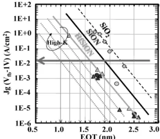
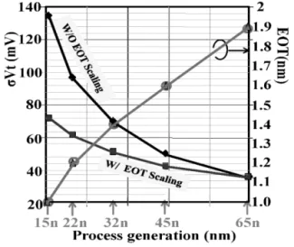
and Lg and Wg are channel gate length and gate width, respectively 1 . When both Lg and Wg are scaled by 0.7, the channel area will be scaled by 0.49 without EOT scaling, the V random variation amount σ will be increased by about 1.43-times. Fig.1 shows the gate leakage scaling for different EOT and gate materials(SiO ,SiON,HfSiON,and other High-). The required EOT depends on the gate material. It can be found that SiON for 1.9nm,HfSiON for 1.6nm, and the new High-k for <1.4nm are needed to suppress the maximum gate leakage Jg (V -1V) to <2E-2 A/cm for low standby power (LSTP) process. Fig. 2 shows the trend of EOT and σ from 65nm to 15nm process generation. The σ could be suppressed to <75mV even when 15nm process node if EOT could be successfully
平成20年11月1日受付
Fig. 1 Gate leakage scaling with different dielectrics and EOT
scaled down, otherwise, it could be increased to >135mV.
2.2 Limit of Design Solutions with Increasing V The increase of σ has led to the degradation in cell stability-and write-margins. Fig. 3 illustrates the design limits. It can be seen that the suppressed WL scheme for SNM assist could become non-practical if σ will becomes>50mV due to the significant Icell reduction by> 70%. If σ is larger than 105mV, the minimum data retention voltage would reach 1.1V. The negative BL scheme and the CVDD-down scheme for WRM assists becomes unable to be adopted any more if σ will become >75mV and >60mV,respectively. The most sen-sitive parameter to σ is the cell current, Icell. If 20% reduction is the limit, often true, allowable σ can only be<40mV and <45mV for 6T and 8T-SRAMs,respective-ly.
3. EXTENTION OF LIMIT OF DESIGN SOLUTIONS
As explained above, a increasing ofσ will place limits on the coverage of each design solution for the margin assists as SRAM is scaled into a deeper nanometer region. There are higher and lower bounds in the design windows for the design solutions and both of them give the impact on each other as a trade-off. For example,a deeper suppressed WL for SNM assist causes to require a deeper negative BL overdriving or CVDD-down for WRM. In this section,the three examples of 1) read modify write decoupled read port 2 , 2) error-checking and correcting (ECC) circuit 3 and 2)V regulation,enabling to relax such kind of limitations are given.
3.1 Write after Read Operation with Decoupled Read Port
As explained above,it is the key to eliminate the require-ments of suppressed WL scheme for SNM in order to relax the excessive requirements of CVDD-down and negative BL for WRM. Having a decoupled read port like 8T-SRAM and read modify write operation becomes the key enabler to do so 2 . Fig.4 shows how each scheme play the key role for extending the limit of design solution as a function of σ . It can be seen that read modify write operation with decoupled read port referred to as 8T+RMW can extend the timing of assist failure for SNM and WRM so that it can not be limited even ifσ becomes >135mV.
A Reviewand Prospect of Area Scaling Trend forSRAM Circuit Design Solution in DeeperNano-meterEra(Yamauchi)
Fig. 3 Figure of merit for various assist schemes Fig. 4 Impacts on each design solution s availability given by read-modify write with decoupled R/W port
Fig. 2 σV scaling trend
3.2 ECC (Error Checking and Correction)for Redun-dancy
If the bit-error rate is r, the probability (p) of an ECC word having two or more defective cells is expressed as: p=1−(1−r) −N×r×(1−r) , where N=(N +N ).
The probability that q redundant words are required is expressed as: P = C ×p ×(1−p) , where W is the total number of ECC words excluding ECC redundant words of R.
As a result, the yield can be expressed as: Y=∑P , where the probability for defects of redundant ECC words of R is neglected for simplicity.
Based on the above equation, ECC impact on yield improvement as a function of the bit-error rate r (which is represented by the number of Z) is calculated as shown in Fig.5,where memory bits is assumed that N=136 consists of N =128 and N =8, W=1024, and R=0∼4.
It can be seen that not only ECC but also ECC+its redundancy can significantly improve the bit-error toler-ance. If R=4,the variation tolerance can be improved by 1.4 of Z, which means the even if σ is increased by 1.4-times due to device scaling to the half (which corre-sponds to about one process generation),the same yield can be maintained. This implies that ECC combined with its redundancy can extend the limit of SRAM scaling by one process generation without EOT scaling.
Fig.6 shows how can each of 1) read-modify write with 8T-SRAM,2) VDD regularity and 3)ECC relax the limita-tions of each design solulimita-tions as a function ofσ .
Fig.7 shows how EOT-scaling can play a key role for SRAM scaling by comparing with the case of non EOT-scaling (shown in upper). It can be seen that if EOT can be scaled down to 1.9nm for 65nm node → 1.6nm for 45nm node → 1.4nm for 32nm node → 1.2nm for 25nm node → 1.0nm for 15nm node, 6T-SRAM can survive with V = 1.2V or ECC V =1.1V without using a read-modify-write operation with 8T-SRAM.
4. AREA SCALING TREND COMPARISON
The design solutions for margin assists including 8T and 10T-SRAM cells are realized at the cost of additional area penalties caused by adding two or four MOSFETs and required associated peripheral circuits. Meanwhile, up-sizing 6T can reduce σ and improve the functional mar-Fig. 5 ECC Impacts on Yield improvement
Fig. 6 Comparisons of SRAM scaling impacts given by each solution
gins at the cost of cell area. In that sense,the area compari-sons of SRAM macro as a function of σ is needed to discuss which design solution including up-sizing 6T becomes better solution for each request.
4.1 Area Comparisons of SNM and WRM Assists As one of examples, up-sizing 6T compares with the suppressed WL depending on how much Icell down can be allowed as shown in Fig.8, which shows the normalized required up-sizing ratio comparisons as a function of σ among 1) up-sizing 6T, 2) suppressed WL (SWL) with allowing 80%Icell down. It can be seen that if 50%-80% Icell down could be allowed, suppressed WL would have greater area-advantage than just up-sizing 6T when σ becomes > 60mV. Meanwhile, when σ is less than 50mV, up-sizing 6T is superior in terms of macro area saving than the suppressed WL due to no need of additional area overhead of peripheral circuits to generate suppressed WL level. In order to highlight which design solutions for SNM and WRM consumes more macro area, Fig.8 shows how much the CVDD-down and negative BL schemes can save the macro area compared with the suppressed WL as a function of σ . It can be seen that WRM assist design solutions of CVDD-down and negative BL consume smaller area than the suppressed WL for SNM and its areas becomes smaller than that of up-sizing 6T when σ becomes > 50mV. In that sense, SNM enhanced cell combined with WRM assist can provide better option than simply up-sizing 6T cell.
4.2 Area Comparisons of 8T and 10T SRAMs Area benefits from the cells with more transistors depend on the following requirements and conditions:1)increasing
cell current, 2) lowering VDD operation,and 3) increasing σ . As a result, there are cross over points if areas of 6T, 8T, 8T with time-multiplexing and 10T are compared as a function of the above conditions as shown in Fig.9.At the initial point, the minimum macro sizes for 10T and 8T are about 1.9-times and 1.4-times larger than 6T, respectively. However, the required conditions like Icell or σ becomes severer, the required area for 6T crosses over 8T first and then 10T as shown in Fig.9.It can be seen that 8T-SRAM combined with time-multiplexing can be smallest at the end of the day if the time-multiplexing (read-modify-write opera-tions) can be allowed. This is due to no need of trade-off among SNM, WRM, and Icell.
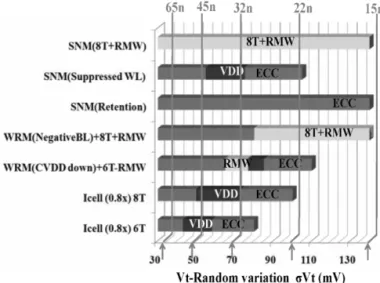
In order to highlight the trend of area advantage as a function of σ Fig.10 shows the normalized required up-sizing ratio comparisons as a function ofσ among 1) up-sizing 6T,2)6T combined with both of negative BL and suppressed WL, 3) 8T combined with negative BL and read-modify-write, 4) 8T combined with negative BL and suppressed WL,and 5)cross-point 10T. It can be seen that simply up-sizing 6T crosses over the two 8Ts combined with negative BL for WRM and read-modify-write and suppres-sed WL for SNM when σ becomes >70mV and >80mV, respectively. 6T combined with negative BL and suppres-sed WL crosses over 8T combined with negative BL and suppressed WL when σ becomes >90mV. 10T crosses over 8T combined with negative BL and suppressed WL when σ becomes >110mV. IfσV could be suppressed less than 70mV thanks to EOT scaling even at a 15nm CMOS generation,6T cells would be allowed long reign as shown in Fig.11.
Fig. 8 Required macro up-sizing comparisons between assist-schemes for SNM and WRM
Fig. 9 Area comparisons of various SRAM cells
4.3 Comparisons of Design Options
As discussed above, many design options have been proposed. However, it depends on the requirements and conditions that which can provide the best performance. Fig.11 shows the concept for which option can become majority in each application. In Fig.11, each application zone is partitioned based on the required the cell current Icell as Y-axis and V range or the amount of σ as X-axis. If V is excessively lowered and σ becomes extremely larger for some applications, cross-point 10T-SRAM or 8T-10T-SRAM combined with read-modify write would be more needed than up-sizing 6T-SRAM as shown in Fig.11 and they would become majority in such region. Meanwhile, if the required Icell is extremely larger for higher-speed application for other applications, 8T-SRAM would become majority even if σ is not extremely larger and V is not excessively lowered, as shown in Fig.11. 6T-A (Asymmetrical 6T-SRAM)also has been proposed 4 targeting for this region, as shown in Fig.11.
5. CONCLUSION
The comparisons of area scaling trend of various SRAM margin-assist solutions for V variability issues have been discussed for the first time. It is found that if the optimistic and pessimistic scenarios for increasing pace of σ are assumed that σ gets <70mV and >130mV at 15nm node, respectively,6T SRAM would be allowed long reign even in 15nm ifσ could be suppressed to <70mV thanks to EOT scaling for LSTP process, otherwise 10T and 8T with read modify write would be needed after σ becomes >85mV and 75mV, respectively.
ACKNOWLEDGMENT
This research is partially supported by a grant-in-aid for scientific research from Japan society for the promotion of science and from computer science laboratory in Fukuoka Institute of Technology.
REFERENCES
[1] M.Pelgrom,A.Duinmaijer,A.Welbers, Matching properties of MOS transistors , Solid-State Circuits, IEEE Journal of vol.24, Issue 5, pp.1433 1439, Oct, 1989.
[2] H. Pilo, J. Barwin, G. Braceras, C. Browning, S. Burns, J. Gabric, S. Lamphier, M. Miller, A. Roberts, F. Towler, An SRAM Design in 65nm and 45nm Technology Nodes Featuring Read and Write-Assist Circuits to Expand Operating Voltage , Digest of Technical Papers, 2006 Symposium on VLSI Circuits, pp.15-16, June, 2006.
[3] K. Itoh, M. Horiguchi, M. Yamaoka Low-Voltage Limitations of Memory-Rich Nano-Scale CMOS LSIs , 33rd European Solid State Circuits Conference, ESS-CIRC 2007, plenary talk, pp.11-13, Sept. 2007
[4] A.Kawasumi,N.Otsuka,T.Yabe,Y.Takeyama,O. Hirabayashi, K. Kushida, A. Tohata, T. Sasaki, A. Katayama, G. Fukano, Y. Fujimura, 21.4 A Single-Power-Supply 0.7V 1GHz 45nm SRAM with a Asym-metrical Unit-β-Ratio Memory Cell IEEE Solid States Circuits Conference 2008, pp.382-383, Feb, 2008
Fig. 11 Comparisons of design options Fig. 10 Area comparisons of various SRAM cell options