Quantum Dot for Fiber In-Line Single Photon
Generation
A thesis submitted by
K. MUHAMMED SHAFI
in fulfillment of the requirements for the degree of
DOCTOR OF PHILOSOPHY
in
SCIENCE
to the
GRADUATE SCHOOL OF INFORMATICS AND ENGINEERING
DEPARTMENT OF ENGINEERING SCIENCE
THE UNIVERSITY OF ELECTRO-COMMUNICATIONS
Tokyo, Japan
on
Thesis Title
Hybrid System of Optical Nanofiber and Single Quantum Dot
for Fiber In-Line Single Photon Generation
Author
K. MUHAMMED SHAFI
Introducing Professor
Prof. Masaru Suzuki
(The University of Electro-Communications, Tokyo, Japan)
Reviewers
Prof. Kohzo Hakuta
(The University of Electro-Communications, Tokyo, Japan)
Prof. Ken’ichi Nakagawa
(The University of Electro-Communications, Tokyo, Japan)
Prof. Jun Nakamura
(The University of Electro-Communications, Tokyo, Japan)
Assoc. Prof. Okuno Tsuyoshi
(The University of Electro-Communications, Tokyo, Japan)
Assoc. Prof. Kali Prasanna Nayak
c
Copyright 2020 by
K. Muhammed Shafi
All Rights Reserved
光ファイバーの一部をサブミクロン直径まで細径化したものをナノ光ファイバーと 呼ぶ。近年、ナノ光ファイバーにより原子等の量子光学応答が様々に操作制御でき ることが実証されている。本論文は、ナノファイバー上に単一の量子ドットを担持 した「ナノファイバー/量子ドットハイブリッド系」を光ファイバー組み込みの単 一光子発生の視点から開発し、その特性を室温から極低温まで研究したものである。 用いた量子ドットは発光中心波長が640nmのコアシェル構造を有するCdSe半導体ナ ノ結晶であり、用いたクライオスタットシステムはナノ光ファイバー系の光透過特 性に何の劣化も与えずに極低温3.7Kまで冷却を行えるものである。量子ドットの発 光特性を室温から3.7Kまで詳細に計測し、その発光は通常の中性励起子と共にイオ ン化励起子によるものであり、かつ中性励起子の発光量子効率は室温から3.7Kまで ほぼ100%であり、一方イオン化励起子のそれは室温においては26%程度であるが5K 以下の極低温においてはほぼ100%になることを示した。また、中性励起子は上準位 が2準位からなる3準位系であるのに対し、イオン化励起子は単純な2準位系であ り単一光子発光系としては中性励起子より有利であることを示した。更に、量子ド ットに極低温下で紫外レーザーを照射することにより量子ドットをイオン化状態に 永続的に転移できることを見出した。これらの結果に基づき「極低温イオン化量子 ドット/ナノファイバーハイブリッド系」を実際にパルスレーザー励起し、その単 一光子発生特性を評価し、高効率で高繰り返しの単一光子発生がファイバーインラ インで実現できることを実証した。
Abstract
Hybrid systems of nanophotonic structures and single quantum emitters have emerged as a promising direction for single photon generation in quantum photonic technologies. Strong confinement of the optical field in nanopho-tonic structures enables photon manipulation far beyond the free space. In this context, tapered optical fibers with sub-wavelength diameter waists, op-tical nanofibers, provide a unique platform. Regarding the single photon generation, a key advantage is the efficient fiber in-line operation, i.e. pho-tons efficiently emitted into the guided-mode of the nanofiber adiabatically couples to that of a conventional single mode optical fiber with near-unity efficiency. Regarding the emitters for quantum photonics, solid-state emit-ters at cryogenic temperatures are preferred from the prospect of practical applications in quantum information technologies.
In this thesis, a hybrid system of an optical nanofiber (ONF) and a sin-gle colloidal CdSe quantum dot (QD) operated at cryogenic temperature is developed and investigated from the viewpoint of fiber in-line single pho-ton generation. Single CdSe core/shell QDs emitting at 640 nm are precisely deposited on the nanofiber surface. An optical cryostat cools the hybrid sys-tem to a sys-temperature of 3.7 K via helium buffer-gas cooling, maintaining the high optical transmission of the ONF (94.5%). The photoluminescence (PL) characteristics of the QDs are investigated by observing the emitted photons through the fiber guided-modes. At 3.7 K, the emission spectrum of the sin-gle QDs showed two distinct narrow zero-phonon lines (∼350 µeV FWHM) compared to the broad spectral width (60 meV FWHM) at room temperature.
upper state of neutral exciton consists of two levels, which effectively results in a fast and slow decay components with decay times of 3.1±0.1 and 153±5 ns, respectively. In contrast, the upper state of trion is one level leading to a single decay process with a decay time of 10.7±0.3 ns.
From the viewpoint of single photon generation, the trion with a single upper level is preferable compared to the neutral exciton. Subsequently, a technique to control the occurrence of trion at cryogenic temperatures is de-veloped. It is shown that the trion occurrence can be manipulated by pho-tocharging the QD by exciting well above the band gap. Most notably, we established a method to create permanently charged QDs with all emissions into the trion zero-phonon line.
Combining the photocharged single QDs in the hybrid system, we evalu-ated the performance of the system as an efficient fiber in-line single photon source. We show that the photocharged QDs exhibit a bright photo-stable emission of single photons with near-unity quantum efficiency, narrow spec-tral width and a fast single decay process. The efficiency of the source is estimated to be 16±2%, with a maximum photon count rate of 1.6±0.2 MHz and a high single photon purity of g2(0)= 0.11±0.02.
The ONF/QD hybrid system could be integrated into the fiber networks paving the way for potential applications in quantum information technolo-gies. The efficiency of the source can be improved by incorporating a cavity structure on the ONF and establish a cavity QED system at cryogenic tem-peratures. Also, the system situation can be extended to various quantum emitters at different wavelengths. We discuss such ideas as future prospects.
Acknowledgements
Learning and research have been a wonderful experience for me. However, none of these would have been possible without the guidance and support of many people.
I would like to express my most sincere thanks to Prof. Kohzo Hakuta for his generous support and guidance during my Ph.D. at the Center for Pho-tonic Innovations. I will remain grateful for his motivations, inspirational suggestions, and constructive criticism, teaching me a lot about doing re-search stringently and presenting the results properly. His deep vision has shaped the thesis into the present form. It was an absolute privilege to learn under his guidance.
I would like to express my sincere gratitude to Assoc. Prof. Kali P. Nayak. I am very fortunate to work with him. Discussions with him was an enjoy-able learning experience for me. His guidance gave me enlightening ideas to improve my thesis and presentation. I appreciate the support and inspiration he gave during my Ph.D.
I would like to thank Prof. Masaru Suzuki for being my "Introducing Professor" to the university. Though we have interacted only towards the end of my Ph.D., his suggestions and comments were very fruitful in writing and improving the presentation of this thesis.
I would like to thank the members of the review committee, Prof. Kohzo Hakuta, Prof. Ken’ichi Nakagawa, Prof. Jun Nakamura, Assoc. Prof. Okuno Tsuyoshi and Assoc. Prof. Kali P. Nayak, for reviewing my thesis. Your suggestions and comments helped me to greatly improve the presentation of
of my time in UEC. I also would like to thank all lab members, Dr. Wei Luo, Dr. Wang Jie, Dr. Yanqiang Guo. I enjoyed being their lab mate. They all helped me to learn new things as well made my stay in Japan very pleasant. I would like to thank Morinaga sensei, Kishimoto sensei, for their com-ments and suggestions in the weekly group meetings.
I would like to thank NS Materials Inc., Japan, for providing us the quan-tum dot samples according to our requirements.
I would like to express my gratitude to Prof. Hema Ramachandran, Ra-man Research Institute, Bangalore, and Prof. V. P. Mahadevan Pillai, Univer-sity of Kerala, India, for showing me the way to the world of research.
Finally, and most importantly, I thank my late parents and other family members for their love and blessings throughout my life. My Special thanks go to the special people in my life Shabna, Nshawa, and Nazmin.
Contents
Abstract vii
Acknowledgements ix
1 Introduction 1
1.1 Quest for an Efficient Single Photon Source . . . 2
1.2 Quantum Nanophotonics for Efficient Single Photon Generation 4 1.3 Optical Nanofiber (ONF) as a Platform for Quantum Nanopho-tonics . . . 7
1.3.1 Confinement of Electromagnetic Field Around an ONF 8 1.3.2 Spontaneous Emission of a Quantum Emitter Around an ONF . . . 9
1.4 Quantum Emitters: Semiconductor Quantum Dots (QDs) . . . 12
1.4.1 Core/Shell QDs as a Single Photon Source . . . 13
1.4.2 Neutral and Charged Excitons in CdSe Core/Shell QDs 15 1.4.3 Linewidth Broadening in QDs . . . 16
1.5 Characteristics of Single Photon Source . . . 17
1.5.1 Purity of Single Photon Source . . . 17
1.5.2 Brightness . . . 19
1.6 Thesis outline . . . 20
2 Experimental Techniques 23 2.1 Fabrication and Characterization of ONF . . . 23
2.3.1 Sub-picoliter Dispenser System and Inverted Microscope 33
2.3.2 Deposition Procedure for Single QDs on an ONF. . . . 34
2.4 Optical Cryostat System for Cooling the Hybrid System . . . . 36
2.4.1 Cryostat System. . . 36
2.4.2 Sample Chamber . . . 38
2.4.3 Cooling Characteristics of the Cryostat . . . 40
2.5 Photoluminescence Measurements . . . 41
2.5.1 Spectral Measurements . . . 41
2.5.2 Photon Correlation Measurement System . . . 42
2.5.3 Time Resolved Photoluminescence Measurement System 43 2.6 Chapter Summary. . . 44
3 Hybrid System of ONF and Single CdSe QDs at Room Temperature 47 3.1 Introduction . . . 47
3.2 Experimental Procedure for Developing the Hybrid System . 48 3.3 Measurement Setup for the Hybrid System . . . 49
3.4 Photoluminescence Emission Characteristics of Single CdSe QDs in the Hybrid System . . . 50
3.4.1 Photon Correlation of Single QDs . . . 51
3.4.2 Emission Spectrum of Single QDs . . . 54
3.4.3 Photon Counting Behavior of Single QDs . . . 55
3.4.4 Photoluminescence Decay of Single QDs . . . 56
3.5 Quantum Efficiency of QDs . . . 57
4 Hybrid System of ONF and Single CdSe QDs at Cryogenic
Temper-atures 61
4.1 Introduction . . . 61
4.2 Experimental Procedure for Cooling to Cryogenic Temperatures 62 4.3 Measurement Scheme . . . 64
4.4 Spectroscopy of Single QDs in the System . . . 65
4.4.1 Temperature Dependence of Emission Spectrum . . . . 65
4.4.2 Spectral Features at 3.7 K . . . 68
4.4.3 Photon Counting and Quantum Efficiency of QD . . . 72
4.4.4 Photoluminescence Decay Measurements . . . 73
4.4.5 PL Decay of Neutral Exciton Emission . . . 74
4.4.6 PL Decay of Trion Emission . . . 75
4.4.7 Temperature dependence of PL Decay . . . 76
4.5 Chapter Summary. . . 80
5 Occurrence Control of Charged QDs 83 5.1 Introduction . . . 83
5.2 Experimental System and Measurement Scheme . . . 84
5.3 Photocharging with 532 nm Excitation . . . 87
5.4 Photocharging with 455, 405 nm Excitation . . . 90
5.5 Photocharging with 355 nm Excitation . . . 92
5.6 Discussion . . . 96
5.7 Chapter Summary. . . 99
6 Single Photon Source Based on the Hybrid System 101 6.1 Introduction . . . 101
6.2 Experimental System and Measurement Scheme . . . 102
6.3 Photocharged QD . . . 104
6.3.1 Polarization Properties . . . 107
Bibliography 119
Chapter 1
Introduction
Quantum information processing and technology have been emerged as one of the main strategic tasks in many countries due to its immense impact and vast potential for applications in diverse fields [1]. The technology has a wide range of applications covering quantum communication, quantum comput-ing, quantum metrology, and quantum sensing [2, 3, 4]. In the context of secure and high-speed communication, a quantum network has been pro-posed, in which the information is carried out by the quantum state of light, single photons [5]. A quantum network consists of several quantum nodes in-terconnected by quantum channels. A quantum node is an interface between the quantum state of light and matter, which can be used for processing and storage of data in quantum states. In contrast, the quantum channels dis-tribute the information over the network via single photons. For the physical implementation of quantum networks, the leading scientific challenge is to attain coherent control over the interaction of light and matter at a single photon level. The existing telecommunication fiber network can serve as an inherent transport medium to transfer the quantum information over a long distance. Therefore, fiber-coupled single photon sources will be a backbone of the future quantum networks [5].
A prime advantage of the quantum network is the security of communi-cation. Quantum key distribution (QKD) or quantum cryptography applies fundamental laws of quantum physics to guarantee secure communication
secret key between two parties using single photons along a quantum chan-nel. The implementation of QKD requires a source that emits only a single photon at a time because the data transfer with more than one photon per bit opens the security loophole like photon-number splitting attacks [12].
Various applications based on quantum networks also require identical single photons. Recently, new QKD schemes have been proposed based on single photon interference, which requires a source of indistinguishable sin-gle photons [13, 14]. Apart from that, applications like quantum teleporta-tion, quantum repeaters, and linear-optical quantum computation [15, 16] are also based on two-photon interference. Therefore the consecutive pho-tons emitted by a single photon source should be identical in all degrees of freedom and exhibit two-photon interference effects. To accomplish this, one needs to ensure that the single photon source is spectrally narrow.
From these deliberations, an important goal can be derived for a future quantum communication technology: the development of an efficient fiber coupled single photon source.
1.1
Quest for an Efficient Single Photon Source
The quest for a single photon source, a light source that emits only one pho-ton at a time with ideal emission characteristics, would be of great benefit to quantum information processing and technology. There have been signif-icant innovations and developments in this direction, albeit an ideal single photon source is yet to be realized [17,18].
From the perspective of applications in quantum information technolo-gies, an efficient single photon source should satisfy the following main re-quirements.
• A high single photon purity. The single photon purity is determined by the second order photon correlation function, g2(τ). For an ideal single photon source, g2(τ= 0)= 0.
• On-demand generation of single photons, meaning only one photon is emitted per excitation pulse, possibly with a high photon count rate. • The photons emitted should be identical in all degrees of freedom, for
example, having the same spectral, temporal profile, and polarization. • Once emitted, all the photons should be collected with high efficiency
into a single-mode optical fiber.
How does one generate a single photon? The first answer would be to take a laser light and attenuate it until the mean number of photons in a given time frame reaches less than one, often called an attenuated laser source. But it is not truly a single photon source as it exhibits finite multi or no photon probability. The most advanced single photon sources are based on sponta-neous parametric down-conversion (SPDC) or spontasponta-neous emission from a single quantum emitter [18,19].
SPDC source is based on frequency down-conversion in a non-linear crys-tal. Correlated pairs of down-converted photons are generated using a high-energy pump photon. The process is non-deterministic, meaning photon pairs are generated in random times, which makes it not suitable for applica-tions requiring photons on-demand. Another critical issue with SPDC source is that the probability for multi-photon events scales up with pump intensity, which limits the purity of the source at high photon generation rate.
tum emitter. The source can have a high single photon generation rate with significantly less probability for multi-photon events [17,18].
There exist various choices for a quantum emitter in terms of operat-ing wavelengths and system efficiency [19, 20]. A good quantum emitter should possess high quantum efficiency, fast decay rate, and narrow spectral width for the emission. Neutral atoms may be an ideal choice for a quan-tum emitter. However, isolating a single atom requires complex experimen-tal systems. From the viewpoint of practical applications, solid state emitters like molecules [21], atom-like defect centers in crystalline host [22, 23], or semiconductor quantum dots [24] are promising choices based on their ex-cellent emission properties and easier techniques to isolate single emitters. Among them, one promising candidate would be semiconductor quantum dots, which can provide wide tunability of emission wavelength with high quantum efficiency [17,18]. However, one of the critical challenges is to col-lect spontaneous emission efficiently.
1.2
Quantum Nanophotonics for Efficient Single
Photon Generation
Regarding quantum emitter based single photon source, one of the key chal-lenges is to efficiently collect the single photons into a single spatial mode, ideally matched to the mode of an optical fiber. One can use an objective lens to collect the emission [25,26]. However, there exists a limitation due to the
achievable confinement of the light field. Moreover, the photons should be coupled to a single-mode optical fiber, which requires stringent alignments. Also, this leads to bulky experimental systems.
Recent progress in quantum nanophotonics has opened a new platform for single photon manipulation with capabilities far beyond the free space [17]. A central goal of quantum nanophotonics is to develop hybrid sys-tems consisting of a single quantum emitter and nano-waveguides so that the single photons can be generated and manipulated. The critical point of such a hybrid system is to confine the electromagnetic field modes to a sub-wavelength region to achieve significant interaction between the electromag-netic field and the quantum emitter.
The advancement of nanofabrication made it possible to structure differ-ent materials like dielectrics, semiconductors, and metals to sub-wavelength dimensions so that the light field can be confined to small sizes. Examples include sub-wavelength diameter nano-waveguides [27], photonic crystal waveguides, [28, 29, 30], plasmonic nanostructures [31, 32] and whispering gallery mode cavities [33,34]. The precise controlling of the position of single quantum emitters can enable the realization of strong light-matter interaction in these systems [35].
Table 1.1: Performance of quantum dot based fiber coupled single photon source. Values in the table are taken from the corresponding reference listed in the same row.
Reference Source efficiency Max. photon rate Photon purity(g2(0))
[26] 8% 89 kHz 0.07 [36] < 1% 11.7 kHz 0.07 [37] 1.4% 84 kHz 0.17 [38] 6% 3 MHz 0.29 [39] 10.9% 2.43 MHz 0.46 [40] 10.7% 2 MHz 0.40
In the context of quantum networks, the coupling of photons into an opti-cal fiber is necessary. It remains a challenge to efficiently couple the photons
of the fiber, and the coupling efficiency is typically poor. Moreover, they are experimentally very challenging.
Table1.1lists the source efficiency, maximum photon rate, and single pho-ton purity of various fiber-coupled single phopho-ton sources based on single quantum dots. The source efficiency denotes the efficiency at which single photons can be produced on-demand. The single photon purity is defined by the second order photon correlation function, g2(0). In most approaches, the source efficiency is typically less than 10%. The maximum reported sin-gle photon rates are moderate in the order of 10 kHz to a few MHz primarily due to the weak coupling into the single-mode optical fiber. For an ideal single photon source, the value of g2(0)= 0. However, for some sources, the g2(0) values are far beyond the ideal value [37, 38,39]. Even though an effi-cient collection of emission from a single quantum emitter into the nanopho-tonic platforms has been demonstrated, coupling to a single-mode optical fiber with high efficiency remains a challenge [37,38]. Therefore, the devel-opment of a robust and efficient fiber in-line single photon source will be a prerequisite for the implementation of the quantum networks.
1.3
Optical Nanofiber (ONF) as a Platform for
Quan-tum Nanophotonics
In the context of strong confinement of light field as well as coupling to single-mode optical fiber, one promising approach would be to use opti-cal nanofibers, tapered optiopti-cal fibers with sub-wavelength diameter waist. In optical nanofibers, the guided field modes are strongly confined to a re-gion with sub-wavelength size, and the nanofiber guided modes adiabati-cally evolve into a single-mode optical fiber.
In the last decade’s optical nanofibers (ONFs), the sub-wavelength di-ameter waist of a tapered silica fiber has opened a promising platform for quantum nanophotonics, paving the way for manipulating single photons in fiber networks. In 2002, Hakuta and co-workers [41] proposed a novel idea of thin tapered optical fiber, where the evanescent field of the sub-wavelength region of the fiber strongly couples with the surrounding medium. Shortly after this proposal, Tong et al. [27] reported the fabrication and novel prop-erties of the sub-wavelength diameter silica wires for photonic applications. Since then, the sub-wavelength diameter waist of a tapered optical fiber has been of great interest to the nanophotonics community [42]. The strong trans-verse confinement of the guided light and long interaction length along the fiber are the key features of ONF.
From a technical aspect, ONF has an advantage over other nanophotonic systems, which is the in-line fiber property. Once a system has been cre-ated on a nanofiber, the system can be naturally integrcre-ated into fiber net-works since the nanofiber guided modes adiabatically evolve to fiber guided modes. Using ONFs diverse quantum optical processes have been estab-lished so far, which includes channeling of fluorescence photons into fiber guided modes [43,44] and laser-cooled atom trapping around ONF [45, 46,
and high single photon purity.
1.3.1
Confinement of Electromagnetic Field Around an ONF
A schematic of light propagation in a nanofiber is shown in Fig.1.1. The nanofiber is fabricated by tapering a commercial single-mode optical fiber. The nanofiber is the sub-wavelength diameter waist of a tapered fiber. Typ-ical single-mode fibers consist of a core with a diameter of around 5 µm, which guides the light and a surrounding cladding with a diameter of 125
µm. After tapering the original single-mode fiber to form a nanofiber waist
region, the core of the optical fiber almost vanishes out, and the clad of the original fiber acts as a core for the nanofiber and the medium outside serves as the clad. Therefore, the refractive index profile of the nanofiber forms a step-index profile in the radial direction with a difference in silica- air refrac-tive index of∼0.45.
It must be noted that due to the thin diameter, the nanofiber guided mode can only support a single fundamental mode (HE11) [49]. A typical mode
profile is shown in Fig.1.1(b). It is evident from the plot that the field in the guided mode is strongly confined in space, and a significant amount of the field lies outside, which is in the evanescent region around the nanofiber. Also, it should be noted that the confinement of the nanofiber guided mode depends on the propagation wavelength (λ) and the nanofiber radius (a).
Figure 1.1: (a) Schematic of an optical nanofiber. In the nanofiber region, light can confine to a sub-wavelength area with a significant evanescent field. The nanofiber guided mode can adiabatically be coupled to both sides of the standard optical fiber. (b) Shows the intensity distribution of the guided mode propagation in the nanofiber waist region for a nanofiber diameter of 310 nm at a wavelength of 650 nm.
1.3.2
Spontaneous Emission of a Quantum Emitter Around
an ONF
The spontaneous emission from a quantum emitter depends on the surround-ing photonic environment. For a higher couplsurround-ing rate of spontaneous emis-sion from a quantum emitter into a guided optical mode, a high density of optical field at the position of the emitter is required. The strong confinement of the guided modes in the nanofiber region leads to a strong light-matter interaction around the nanofiber. As a consequence, the spontaneous emis-sion of a quantum emitter around the nanofiber is strongly modified and en-hances the coupling of the spontaneous emission into the nanofiber guided mode [43]. The following section provides the theoretical understanding of the relation between optical modes and spontaneous emission with an em-phasis on channeling efficiency into the nanofiber guided modes.
Purcell first discussed the modified spontaneous emission of an atom in a cavity in the microwave regime [52]. The Purcell factor quantifies the en-hancement of the spontaneous emission rate. According to Fermi’s Golden
Figure 1.2: Schematic diagram showing the modified spontaneous emission of an emitter around the nanofiber. γ(g)is the decay rate into the nanofiber guided mode and γ(r)is the decay rate into the radiation mode.
rule [50], the spontaneous emission rate (Γ) is given by,
Γi f =
2π
¯h |<i|Mi f|f >|
2
σ(vi f) (1.1)
where Mi f is the transition metrix element between the initial and final
en-ergy state, and σ(vi f) is the local mode density of the optical field at the
transition frequency vi f. Modifying the environment of a quantum emitter
changes the strength of the optical field density and thereby can tailor the spontaneous emission rate.
For an emitter placed close to the nanofiber surface, the local density of the optical field is modified by the presence of the nanofiber, which mod-ify the spontaneous emission rate of the emitter. Due to this, a significant amount of emission from an emitter can be channeled into nanofiber guided modes. Figure 1.2 display the schematic diagram of the modified sponta-neous emission of an emitter around the nanofiber. A theoretical investiga-tion on the effect of the spontaneous emission rate of a multi-level Cs atom in the vicinity of a nanofiber can be found in Ref. [43].
Here we consider a two-level atom positioned on the surface of nanofiber and is prepared in the excited state, and the field is initially in the vacuum state. In this case, the total decay rate (Γ) is the sum of decay rate into a guided mode (γ(g)) and radiation mode (γ(r)) as given below.
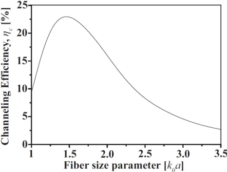
Figure 1.3: Channeling efficiency (ηc) of spontaneous emission into nanofiber guided
modes. ηcas a function of fiber size parameter (k0a). The figure is reproduced from
Ref. [53].
Γ=γ(g)+γ(r) (1.2)
The channeling efficiency (ηc) into the nanofiber guided modes can be
expressed as ηc = γ (g) Γ = γ(g) γ(g)+γ(r) (1.3)
In order to quantitatively understand the channeling of spontaneous emis-sion into the nanofiber guided modes, ηc as a function of fiber size
parame-ter (k0a) is plotted in Fig. 1.3, where k0 is 2π/λ and a is the radius of the
nanofiber [53]. From Fig. 1.3, it can be seen that the ηc is sensitive to k0a
and depends on the propagation wavelength and the diameter (2a) of the nanofiber. The channeling efficiency is determined by the confinement of the nanofiber guided modes. It is obvious for a thick fiber that the confinement is weak. Moreover, when the fiber is very thick compared to the wavelength,
fore, there exists an optimum diameter for which the confinement and chan-neling efficiency can be maximum. As seen from Fig. 1.3, a maximum value of channeling efficiency ηc= 22% occurs for a fiber size parameter k0a= 1.44
[43]. For an emission wavelength of 650 nm, the optimum nanofiber diame-ter will be around 300 nm.
1.4
Quantum Emitters: Semiconductor Quantum
Dots (QDs)
Various quantum emitters have been investigated for developing a potential single photon source, which includes atoms [54], molecules [21], and solid-state emitters [17,55]. Regarding the emitters for quantum photonics, solid-state emitters are preferred from the viewpoint of developing hybrid systems for practical applications in quantum information technologies. Various hy-brid systems utilizing solid-state emitters have been developed so far using atom-like defect centers in diamonds [22], 2D materials [23], and quantum dots [56,39]. Among them, one promising candidate would be semiconduc-tor quantum dots, nanometer-scale crystals containing core/shell structures in colloidal solution, which can provide tunability of emission wavelength with high quantum efficiency. Moreover, the colloidal quantum dots are easy to integrate into any nanophotonic structures. In this section, we will focus on the general properties of core/shell semiconductor quantum dots in col-loidal solutions.
Figure 1.4: (a) Schematic representation of a core/shell QD. (b) Schematic energy level diagram of electrons and holes confined in a QD. The optical transition is shown by a red arrow. Ebulk, Egapare the bandgap of the bulk semiconductor
mate-rial and QD, respectively.
1.4.1
Core/Shell QDs as a Single Photon Source
Colloidal QDs are nanometer-sized crystals consisting of semiconductor ma-terial as core and capped with another semiconductor mama-terial of higher bandgap as shell and a covering of ligands. QDs exhibit size-dependent con-finement of excited-state electron and hole wave functions and form only discrete energy levels [57]. Therefore QDs are generally referred to as "ar-tificial atoms," and they emit like real atoms in terms of emission photon statistics [24]. QDs emission properties can be engineered by controlling their size or composition to modify the emission energy and the nature of the transitions, which make them a promising and versatile system. The first nanocrystals based on only cadmium selenide (CdSe) had various limitations in their photo-stability and emission quantum efficiency (QE) [57]. The sur-face passivation using higher bandgap materials like cadmium sulfide (CdS) and zinc sulfide (ZnS) resulted in a core/shell architecture for the colloidal QDs as sketched in Fig. 1.4(a). The core/shell architecture improved the photo-stability, and nearly 100% QE was reported [58,59].
The most pertinent properties of colloidal semiconductor QDs originate from the spatial confinement potential due to the nanometer size of the QDs. To get a view about the effect of spatial confinement, let’s consider first the
size of the semiconductor material is smaller than the Bohr radius, Coulomb interaction becomes stronger and spatially confined electron-hole pair form an exciton. As a consequence of the confinement, the energy levels in the conduction and valance band become quantized. Brus et al. [60] provided a model for quantum confinement effect in QDs, which gave the expression for the energy of bandgap of QD (Egap) based on the material being used and
its bandgap in bulk form.
Egap =Ebulk+ π 2¯h2 2R2 [ 1 me + 1 mh ] −1.8e 2 eR (1.4)
where Ebulk is the bandgap of the bulk material, ¯h is the Plank’s constant, R
is the QD radius, meis the effective mass of the electron of the material, mhis
the effective mass of hole of the material, e is the charge of an electron and e is the dielectric constant of the material. The second term in equation1.4is the quantum energy of localization, and the last term is the Coulomb attraction; both terms depend on the QD radius. The energy of the bandgap increases with decreasing the QD radius due to the stronger quantum energy of local-ization compared to the Coulomb attraction, which is the reason behind the size-dependent optical properties of the semiconductor QDs.
Single semiconductor QDs have proven to be an ideal source of single photons under both optical and electrical excitations [24, 26]. Figure 1.4(b) display the schematic energy level diagram of electrons and holes confined in a QD. In a photoluminescence event, an absorbed photon excites an electron from the valance band to the conduction band, leaving behind a hole; both
charge carriers quickly relax to the band-edges. The radiative recombination of electron and hole in a single QD results in the emission of a photon with an energy equivalent to the difference between the lowest initial and final ex-citonic states [61]. The recombination of electron and hole has a characteristic decay time, which depends on the radiative and non-radiative decay rates. The emission of a photon happens only after a finite decay time. Therefore the QD can be populated again with the charge carrier only after this decay. Hence only one single photon can be emitted at a given time, which makes the single QD as an ideal source for single photons [62]. On-demand sin-gle photons can be generated from a sinsin-gle QD under the pulsed excitation scheme [24].
1.4.2
Neutral and Charged Excitons in CdSe Core/Shell QDs
Recent spectroscopic studies on colloidal CdSe core/shell QDs revealed that the QD emission occurs not only from neutral exciton state but also from a photocharged state known as trion state [63, 64]. Trion has an extra charge carrier along with an electron-hole pair (exciton). That is, it has two electrons in the case of negatively charged QDs or two holes in the case of positively charged QDs. Trion emission has been observed from single CdSe QDs with thick shell or gradient thick shell structure [65,66] and the PL emission from these QDs switches between exciton and trion. At room temperature, the photon counting behavior of PL emission from the single QDs showed two-step like behavior due to the difference in QE of the two emitting state. Trion has a less QE at room temperature, but it has been observed that the trion QE has improved to 100% at cryogenic temperature by using thick shell or a gradient shell QDs with CdS or CdS/ZnS shell [66,67].
Γ= ¯h
τ (1.5)
Assuming a typical lifetime of τ = 40 ns for CdSe QDs [63], we get a linewidth Γ of 0.017 µeV.
Due to the quantized energy levels in QDs, one would expect to see a sharp spectral line corresponding to the energy difference between the levels. However, in experiments, the emission spectrum of single QDs was observed to be highly broad due to the dephasing mechanisms [68,69]. At room tem-perature, a spectral width of around 20 nm FWHM (60 meV) was observed, due to spectral diffusion and carrier-phonon coupling. Spectral diffusion is mainly caused by the charge fluctuations in the local environment of the QD, which induces a shift in the band-edge due to the Stark effect [68,70]. Since solid state emitters are hosted in a crystal, and they interact with the crys-tal lattice. The probability of the coupling process to phonon scales strongly with temperature, such that a significant increase in spectral width can be observed in experiments. Both these effects contribute to the broadening of emission spectrum.
To achieve narrow emission spectral width and indistinguishable photons from QDs, operation at cryogenic temperature is inevitable. The research demonstrated in this thesis is carried at cryogenic temperatures for gener-ating single photons with narrow spectral width from semiconductor CdSe core/shell QDs.
-400 -200 0 200 400 0.0 0.5 1.0 1.5 2.0 g 2 ( ) Delay time, Super- Poissonian Poissonian Sub- Poissonian
Figure 1.5: Second order correlation function g2(τ)for photons from three different
light sources. A thermal source (supper-Poissonian), laser source (Poissonian) and single photon source (sub-Poissonian).
1.5
Characteristics of Single Photon Source
In this section, we explain the performance metrics used to evaluate a sin-gle photon source, later on, utilized to experimentally determine the perfor-mance of the hybrid system developed for fiber in-line single photon gener-ation.
1.5.1
Purity of Single Photon Source
The purity of a single photon source is determined based on the statistics of photon arrival time distribution. Photon statistics relate how the num-ber of photons emitted by a light source behaves, how the photons are cor-related with each other, and how properties of these photons vary [71, 72,
g2(τ) = hI1(t)I2(t+τ)i
hI1(t)ihI2(t+τ)i (1.6)
where I1(t) and I2(t+τ) are the intensities of light reaching at detector 1
and 2 at time t and t+τ respectively and the angular brackets denote the
time averaging. g2(τ) is the correlation of intensities or the number of
pho-tons arrived at detectors. It has been theoretically and experimentally shown that the g2(τ =0) for photons from a thermal source (super-Poissonian
dis-tribution) is 2, implying correlated or bunched emission of photons [73,74] as shown in Fig. 1.5 by the blue curve. It has a unit value for a coherent source (Poissonian distribution) as plotted in Fig. 1.5 by the yellow curve. In case of a single photon source (sub-Poissonian distribution) g2(τ = 0) is
0 [75], which means that only one photon is emitted at a time, signifying anti-bunching and this determines the purity of single photon source. The behavior of g2(τ) versus τ is shown in Fig. 1.5by the red curve. However,
the value of g2(τ)for all sources approaches unity for long time delays.
A practical single photon source shows a strong anti-bunching dip close to zero at zero time delay, and such measurement results are considered as proof that the emission originates from a single quantum emitter. The g2(τ)
can be measured by employing a Hanbury-Brown Twiss setup [76], where the photons are split using a 50:50 beam splitter and send into two single pho-ton counting modules (SPCMs). The time-stamped arrivals of phopho-tons are then recorded by means of a time-correlated single photon counter. The mea-surements of the normalized correlation/coincidence of photons between the
two SPCMs yield the value of g2(τ). In the photon counting mode, the
ex-pression of g2(τ) in terms of coincidence is [73] is given by the following
expression,
g2(τ) = NcT
N1N2τc (1.7)
where τ is the time delay between the arrival of photons at the two SPCMs, N1, N2, Ncare the number of photons at SPCM 1, SPCM 2 and the coincidence
counts respectively. T is the total acquisition time, and τc is the coincidence
time window. The ability of a single colloidal CdSe quantum dot to emit a single photon is established using this procedure. In terms of the number of emitters, the normalized correlation function at τ =0 is expressed by the relation, g2N(τ = 0) =(N−1)/N, where N is the number of emitters. If the
value of g2(τ = 0) is exactly zero, then it reflects that the emission occurs
from a perfect single emitter.
1.5.2
Brightness
The brightness or the source efficiency of a single photon source can be de-fined as the probability with which the source emits a single photon once triggered. The experimental value of the brightness of a single photon source can be measured using the maximum photon count rate (ΓSP) of the emitter
under pulsed excitation with a repetition rate of R. By normalizingΓSPto the
R at which the source is triggered, we can estimate the average number of photons emitted per excitation pulse. It should be noted that the maximum photon count rate is limited by the repetition rate of the laser. Correcting for the detection efficiency of the setup (α), the brightness (β) of the source can be defined as,
β= ΓSP
1.6
Thesis outline
The scope of this thesis is to focus on the development and spectroscopy of a hybrid system of an optical nanofiber and a single quantum dot from the viewpoint of fiber in-line single photon generation, which is organized as fol-lows.
Chapter 2: Presents the experimental techniques used for developing the hybrid system of ONF and a single QD. This chapter begins by explaining the realization of ONF, followed by the technology used for depositing sin-gle CdSe QDs on ONF. The design of custom-designed optical cryostat and spectroscopy techniques is described at the end of the chapter.
Chapter3: The development of a hybrid system of an ONF and single CdSe QD is presented. The emission characteristics of single CdSe QDs at room temperature are investigated through the fiber guided modes from the view-point of single photon generation.
Chapter4: we explain the development and characteristics of a hybrid sys-tem of ONF and single CdSe QDs, which is operated a cryogenic sys- tempera-ture of 3.7 K. We systematically investigated the emission characteristics of single QDs in the hybrid system by observing the emitted photons through the fiber guided modes. We experimentally show that for quantum photonic applications, charged exciton (trion) is superior to neutral exciton at cryo-genic temperatures.
Chapter5: A method to control the occurrence of trion in a single CdSe QD optically at cryogenic temperatures is presented. We used a hybrid system
of ONF and single QD at cryogenic temperature and systematically inves-tigated the photocharging behaviors of CdSe QDs by varying the excitation laser intensity and wavelength. Most notably, we have established a method to create permanently charged QDs as long as the cryogenic conditions are maintained.
Chapter6: Presents the development and performance of an efficient fiber in-line single photon source based on a hybrid system of a photocharged sin-gle QD on an ONF at cryogenic temperature.
Chapter7: The results are summarized, and an outlook to the future prospects is presented.
Chapter 2
Experimental Techniques
The experimental results presented in this thesis were collected from differ-ent experimdiffer-ental setups using various technologies. This chapter will explain the experimental techniques used for the development and the spectroscopic studies of the hybrid system of ONF and a single QD. The experiments were carried out both at room temperature and at a cryogenic temperature of 3.7 K. This chapter will begin by explaining the realization of ONF, followed by the technology used for depositing single CdSe QDs on ONF. The design of an optical cryostat system and spectroscopy techniques are described at the end of the chapter.
2.1
Fabrication and Characterization of ONF
ONFs were experimentally realized by adiabatically tapering commercial single-mode optical fibers using heat and pull technique with a transmission of > 99% [27, 77,78, 79]. A schematic diagram of the fiber taper is shown in Fig.2.1. The nanofiber region is located in the central region of tapered fiber. A typical fiber consists of 125 µm diameter with core and clad. By heating and pulling, the original fiber is tapered down to a few hundred nanome-ters, and the core almost vanishes out to form the uniform waist region. It is important to note that in the region where the core begins to vanish, the fiber mode transitions from a core guided-mode to a clad guided-mode. It
Figure 2.1: Schematic of a tapered optical fiber, the central uniform waist is the nanofiber region, L. R0, z0, represents the original fiber radius and stretched
dis-tance, respectively.
should also be noted that the original core guided-mode should be adiabati-cally coupled to the clad guided-mode for the minimal optical loss.
2.1.1
Design of ONF
The adiabatic tapering condition ensures that the transition of fundamen-tal core-mode to fundamenfundamen-tal cladding-mode (nanofiber mode) takes place without any loss of power to higher-order cladding-modes. In the nanofiber, the fundamental mode (HE11) of the optical fiber is automatically coupled to
the mode of the nanofiber with minimal optical loss, and it is achieved by adiabatic criteria for the tapering angle [80]. The idea is to change the fiber diameter slowly along the propagation direction of the light such that all the optical power remains in the fundamental mode (HE11) while the coupling
to other modes is suppressed. The adiabatic tapering condition is given by,
| dR
dz |= R
2π[β1(z) −β2(z)] (2.1) where R and dRdz are the radius and taper angle at a specific point. β1(z)and
β2(z) are the propagation constants of the fundamental mode and the next
higher-order mode with the same symmetry. When the wavelength and di-ameter satisfy the single-mode condition for nanofiber, only the fundamental mode can propagate through the nanofiber. However, the tapered region can
support higher-order modes, which results in transmission loss. The tapering angle suggest a typical profile for the tapered fiber. In a heat and pull tech-nique one can control the profile of the nanofiber by controlling heat zone and stretching distance of the fiber.
If a commercial silica fiber with a radius R0 is heated with a fixed heat
zone of length L (scan length of flame) and stretched through a distance of 2z0, a uniform waist region of smaller radius R(z0)with a length L is created
at the center with a taper region on either side. The taper profile function is given by the equation2.2, which follows a decaying exponential profile [77],
R(z) = R0e−z/L (2.2)
The heat zone length and stretching distance decide the radius of the nanofiber. Also, the uniform waist length of nanofiber is equal to the scan length.
2.1.2
Fabrication of ONF
Heat and pull technique is the standard way for fabricating ONFs, where a section of a commercial optical fiber is heated and pulled in a programmed way. Heating of the fiber section is achieved by different methods such as flame brushing using hydrogen and oxygen gas [81], micro-ceramic heaters [82], CO2 laser heating [83, 84], etc. The methods mentioned above have
their own merits and demerits. We use a flame brushing technique because of its versatility in taper design and the ability to produce ONFs with better transmission.
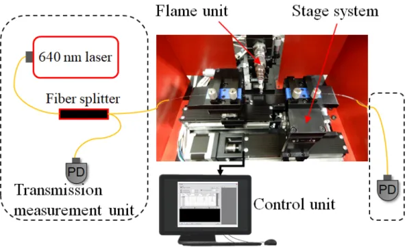
Figure 2.2 shows the schematic of the fabrication setup. The ONFs fab-rication system consists of four main elements [85]. (i) two synchronized stage systems, (ii) flame unit, (iii) control unit, and (iv) transmission measure-ment unit, and all systems are fully automated and computer-controlled. The
Figure 2.2: Schematic layout of the ONF fabrication system, the dashed box shows the transmission measurement unit. The flame unit, stage system and control unit are indicated in the photograph.
whole system is inside a clean booth equipped with a high-efficiency partic-ulate air (HEPA) filter-based air cleaner. More details of the system can be found in the Ref. [86]. The stretching distance and scan length are deter-mined by the four input parameters of the stage system which are (i) swing width (SW), (ii) swing speed (SS), (iii) stretching speed (StS), (iv) stretching distance (StD).
We used commercial single-mode fibers (SM 600, Fibercore, fiber diame-ter: 125.7 µm, cut-off wavelength: 519 nm, mode field diamediame-ter: 4.3 µm) for the ONF fabrication. The polymer coating (jacket) from some section (5 cm) of the fiber was removed by keeping in acetone for about 15 minutes. We use a procedure where the flame is stationary, and the two stages holding the fiber section oscillate and stretch inside the flame of hydrogen-oxygen gas.
Since we use the quantum dots with an emission wavelength of 650 nm, the channeling efficiency has the highest value for a fiber size parameter of 1.44, which corresponds to a nanofiber diameter of 310 nm. Therefore fab-ricate the nanofiber with a diameter of 310 nm and a uniform waist length
Table 2.1: Typical parameters for producing ONFs with uniform waist length of 2.5 mm and diameter 310 nm. SW, SS, StS, StD represents swing width, swing speed, stretching speed, stretching distance, respectively.
Step SW (mm) SS (mm/sec) StS (mm/sec) StD (mm)
1 5.5 3.2 2 0
2 5.5 3.2 0.2 4.81
3 5.5 3.2 0.1 11.68
4 5.5 3.2 0.2 32.4
5 2.5 3.2 0.48 48.05
of 2.5 mm by using a 5 step process.Table 2.1 lists the parameters such that the adiabatic condition was satisfied for minimal transmission loss. In the first step, the flame brushes on the fiber with a 5.5 mm swing width (SW) at a swing speed (SS) of 3.2 mm/sec without stretching. The stretching was started from the second step onwards while the flame brushes on the fiber with the corresponding swing width and the fiber was stretched to a length of 48.05 mm to achieve the desired nanofiber diameter. The stretching dis-tance determines the nanofiber diameter, whereas the speed and amplitude of oscillation control the taper shape.
2.1.3
Transmission and Diameter Measurements of ONF
To measure and monitor the transmission of ONF, a 650 nm laser was sent through the fiber while heating and pulling the fiber. The transmission mea-surement unit is shown in the Fig. 2.2. For better accuracy of measurement, the light from the laser is split into two via fiber beam splitter, where one of them was sent to a detector for reference and the other to another de-tector through the fiber, which was used for ONF fabrication. The simul-taneously recorded reference and the signal during the heating and pulling process yields the transmission profile of the ONF. Figure 2.3 display the transmission profile of ONF, measured during the fabrication process. The effective single-mode transmission after the fabrication was estimated to be 99.1±0.1%. The transmission drop around 150 sec represents the core-mode
0 100 200 300 80 85 90 T r a n sm i ssi Time (s)
Figure 2.3: Transmission characteristics of ONF measured during the heating and pulling process. ONF transmission after the fabrication was estimated to be 99.1±0.1%.
cut-off transition region where the core begins to vanish and the fiber mode transitions from a core guided-mode to a clad guided-mode, which is strongly confined by the silica–vacuum interface (vacuum-clad fiber).
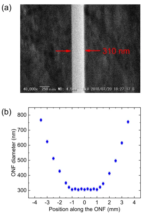
The diameter profile of the fabricated ONF was measured using a scan-ning electron microscope (SEM)(Keyence VE-9800). The ONF was gently mounted on a metal plate using UV curable glue and sputtered with a few nanometer layers of platinum. The sputtering helps to prevent the charg-ing up of the ONF due to the electron beam of SEM. The images at different positions along the ONF with a step of 0.25 mm were taken by placing the sample in SEM. A typical SEM image of the ONF with a diameter of 310 nm is shown in Fig. 2.4(a). These images were analyzed to determine the diam-eter profile of the ONF. Figure 2.4(b) shows the measured diameter profile of 310 nm ONF. Each data point in Fig. 2.4(b) corresponds to the average
-4 -3 -2 -1 0 1 2 3 4 300 400 500 600 700 800 O N F d i a m e t e r ( n m )
Position along the ONF (mm)
(b) (a)
310 nm
Figure 2.4: Characteristics of the fabricated ONF. (a) SEM image of an ONF with a diameter of 310 nm. (b) Measured diameter profile of the ONF.
of measured diameter in the same image with a standard deviation as error bars. The fabricated nanofiber has a uniform waist diameter for a length of 2.5 mm with a waist diameter of 310 ±10 nm. The diameter and transmis-sion were reproducible within the experimental error for the designed ONF pulling parameters.
Figure 2.5: Photograph of the ONF holder.
2.1.4
Design of Holder for ONF
The holding structure for ONF was carefully designed for compatibility with the experimental systems. Since most of the experiments were performed at cryogenic temperature, the holder was made of silica and invar to min-imize the thermal contractions due to the cooling. Figure 2.5 display the photograph of the holding structure with ONF. The holder has a U- shaped design with an opening length of 70 mm for the optical access. The ONF was mounted straight between the two arms of the holder. The ONF was fixed to the V-groove of the U-shaped holder by mechanically fixing it with a piece of silica structure at the top edge of each U-pillar. Mechanical fixing with silica plate was chosen to match the expansion coefficient of the fiber and to make sure that the tension on the fiber is minimum during the cooling process.
2.2
Characteristics of CdSe Core/Shell Colloidal QDs
For the experiments demonstrated in this thesis, we used CdSe QDs with a thick gradient shell of CdS and an outermost ZnS shell in the toluene col-loidal solution. The QDs were synthesized in lab-scale in collaboration with a Japanese company, NS materials, Inc.
Figure 2.6: CdSe core/shell colloidal QDs. (a) Scanning electron microscope image of the QDs. (b) Absorbance spectrum of QDs in toluene colloidal solution, in the inset an enlarged view of the band-edge absorption is shown.
Core/shell structured QDs with thick and gradient shells, which emit 640 nm fluorescence, were synthesized using an improved method described in Refs.[87, 88]. The core structure of the QDs mainly composed of cadmium (Cd) and selenium (Se) was first synthesized by reacting a Cd based com-pound and Se at a high temperature above 250◦C in non-polar organic sol-vents. The QD-core was separated by precipitation with ethanol, followed by centrifugation (7,500 rpm) to purify the QD-core. Protection of the CdSe-core with an inorganic shell was performed by reacting zinc (Zn) based com-pounds and sulfur (S) at a high temperature above 280◦C. The reaction was repeated at least two times to generate a thicker and gradient shell structure of more than 5 nm thickness. The core-shell structured QD was purified by a combination of precipitation and centrifugation (7,500 rpm), then stored in toluene. The QE of the QDs was measured as 85±5% in a colloidal solution using an integrating-sphere photometer.
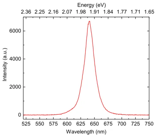
Figure2.6(a) shows the scanning electron microscope image of the synthe-sized thick gradient shell QDs. The average size of the single QDs is less than 10 nm. The ensemble absorption spectrum of QDs is plotted in2.6(b), and an enlarged view around the band-edge is shown in the inset (black curve). The band-edge absorption occur at 631 nm (1.96 eV). Figure2.7 display typical
525 550 575 600 625 650 675 700 725 750 0 2000 I n t e n s i t y W avelength (nm)
Figure 2.7: Emission spectrum of a single CdSe QD at room temperature.
emission spectrum of a single QD at room temperature. The central wave-length of PL emission spectrum is 640 nm (1.94 eV) with an FWHM of 20 nm (61 MeV). The emission spectra of single QDs in the sample shows a relative shift due to the size distribution of QDs in the colloidal solution.
The broad emission spectral width of the single CdSe QDs makes them less preferable for applying such QDs to photonic applications. But this fee-ble factor can be overcome by extending the working temperature to cryo-genic temperatures, and it is one of the main objectives of this thesis. At cryogenic temperature, the narrowing of spectral width could be expected.
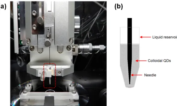
Figure 2.8: Sub-picoliter needle dispenser system. (a) Photograph of the needle dis-penser system installed on an inverted microscope. (b) Schematic illustration of the needle and the liquid reservoir.
2.3
Precise Deposition of Single CdSe QDs on an
ONF
Deterministic and precise deposition of single solid-state quantum emitters on nanophotonic structures is essential for real application in quantum in-formation science. Until now, various techniques have been developed for depositing single solid-state emitters, especially on the nanofiber [56,89,90]. We developed a sub-picolitre needle dispenser system to deposit single CdSe QDs deterministically on the nanofiber. The experimental system and the procedures are detailed in this section.
2.3.1
Sub-picoliter Dispenser System and Inverted
Micro-scope
We developed a sub-picoliter needle dispenser system installed on an in-verted microscope for depositing the single QDs on the nanofiber. Figure
direction, and the whole system is installed on a separate X-Y-Z microme-ter stage. The function of the glass tube is to act as a reservoir for the QD solution. We used a tungsten needle with a tip diameter of 5 µm so that it dispenses only a small amount (pico-liter volume) of the QD solution.
To manipulate the position of the nanofiber, we used an inverted micro-scope (Nikon, Eclipse Ti-U) [91] with a high precision X-Y translation stage (Sigma koki, FC-401G) [92]. The precision stage has a travel range of ±15 mm from the center with a step resolution of 50 nm, which is controlled by the computer. The microscope has two input ports having beam splitters (60 (T):30 (R)), one is for QD excitation, and the other is for white light illumi-nation. The microscope is equipped with objective lenses of different mag-nification (5X, 10X, 20X, 40X) for excitation and imaging along with a CCD camera. The whole system is inside a clean booth equipped with a HEPA filter-based air cleaner.
2.3.2
Deposition Procedure for Single QDs on an ONF
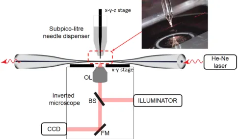
Single CdSe QDs are deposited on the ONF using the computer-controlled sub-picoliter needle dispenser. Fig. 2.9 shows the schematic of the mental system. An ONF with a diameter of 310 nm is used for the experi-ments, which is fixed to the X-Y stage on the microscope. The central part of the nanofiber is located and imaged on the CCD using an objective lens. A tungsten needle with a tip size of 5 µm was used for the experiment to get a very localized spacial control on the ONF. The objective axis is fixed and
Figure 2.9: Schematic diagram of the experiment. OL, BS, and FM are objective lens, beam splitter, and flipper mirror, respectively
the needle axis is adjusted to coincide with the axis of the objective lens us-ing the X-Y of the micrometer stage. The glass tube filled with CdSe QDs in toluene colloidal solution (concentration of 1013 dots/cm3) acts as the reser-voir of QDs solution for the deposition. The glass-tube end was set 100 µm above the nanofiber.
A He-Ne laser was sent through the ONF prior to the QD deposition to monitor the process. The contact between the needle tip and nanofiber was controlled via computer by monitoring the scattered laser light from the nanofiber through a CCD camera. Once the needle tip passes through the glass tube containing the QD solution, it carries a small amount at its edge, and the needle tip was allowed to touch the nanofiber surface to deposit a single QD. The speed of the needle was adjusted to 100 µm/s so that the tip could touch the nanofiber surface before toluene on the tip dried up. After the needle touches the nanofiber surface for 10 ms, the needle tip was moved back into the glass tube. The spatial accuracy of the QD deposition along the nanofiber axis was estimated to be 0.4 µm. The above process allows QDs to be deposited very precisely with a success probability of about 60% for single QD deposition for each trial.
Figure 2.10: Schematics of the cryogenic system and the associated components.
2.4
Optical Cryostat System for Cooling the
Hy-brid System
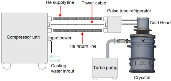
An optical cryostat was designed and build aiming to cool the hybrid sys-tem of an optical nanofiber and single quantum dots. The uniqueness of the cryostat is that the hybrid system is cooled down to 3.7 K via He buffer-gas cooling. The following sections describe each component of the setup.
2.4.1
Cryostat System
Figure2.10display the schematic of the cryogenic system and the associated components. The cryostat exhibit an elongated aluminum chamber consist of a two-layer structure and a sample chamber made of copper. The cryo-stat chamber can be opened from underneath, and the sample chamber is fixed to the bottom of the cold plate. The two-layered heat shield surround-ing the sample chamber protects from black-body radiation. There are fused silica glass windows mounted on the side of the sample chamber and the shields to provide optical access to the sample chamber. The whole cryostat is mounted and hanging on a support frame, which is fixed to the optical table. A vacuum value connecting to the inside of the cryostat is provided at
Figure 2.11: Photographs of the cryogenic system (a) Front View of the cryostat and cold head. (b) Bottom view of the cryostat showing the sample chamber attached to the cold plate
the top to evacuate the cryostat. The photographs of the cryostat are shown in Fig. 2.11. Figure2.11(b) display the bottom view of the cryostat showing the sample chamber attached to the cold plate.
The cryostat can be cooled down to 3.7 K by a pulse-tube refrigerator (RP-082B2S, Sumitomo Cryogenics). The pulse-tube refrigerator consists of a cold head, valve unit, and a compressor. The main function of the cold head is to produce continuous closed-cycle refrigeration at temperatures, depend-ing upon the heat load imposed. The cold head is attached to the cryostat through a metal expansion joint. The cold head is mounted on a support frame, which is fixed to the ground to reduce the effect of vibration. The key factors which distinguish the pulse-tube refrigerator from the conventional cryocooler are that it has no moving part in the cold head and generates less vibration, which is essential for the nanophotonics experiments. The cold
Fiber feedthrough
He gas pipe Sample Chamber
ONF Holder
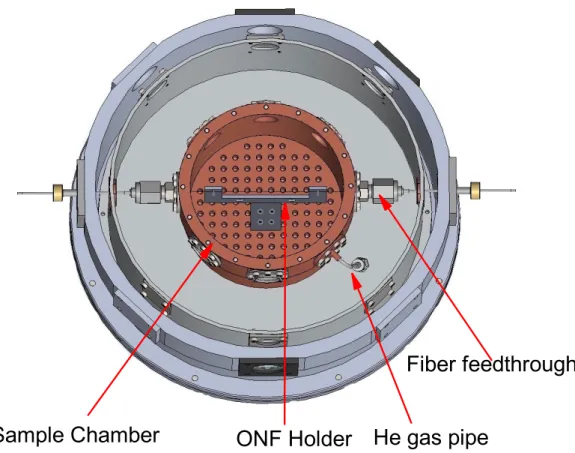
Figure 2.12: Cross sectional view of the cryostat showing the copper sample chamber
head of the refrigerator is driven by a He compressor (F-70, Sumitomo Cryo-genics) in closed-cycle mode, and the compressor is water-cooled. The sup-ply pressure of He in the compressor is maintained at 15 bar. The function of the compressor is to provide the high-pressure He-gas and power to the cold head.
2.4.2
Sample Chamber
The sample chamber underneath the cold plate has an inside diameter of 13 cm and a height of 10 cm. Fig.2.12shows the cross-sectional view of the cryo-stat showing the sample chamber. The sample chamber has a feedthrough pipe, which is used to evacuate the sample chamber and to fill the sample chamber with He buffer-gas at a pressure of 15 kPa at room temperature. The sample chamber also has two feedthroughs for optical fiber access along
0 2 4 6 8 0 100 200 300 Time (hour) T e m p e r a t u r e ( K ) 3.7 K
Figure 2.13: Cooling characteristics of the cryostat versus time
an axis. All the feedthrough are vacuum-sealed using vacuum coupling ra-diation (VCR) metal gaskets. A temperature sensor and a heater are placed at the inside bottom of the chamber.
The hybrid system of ONF and single QDs can be installed into the sam-ple chamber. Both ends of the fiber are then taken outside through the fiber feedthrough, which is vacuum-sealed using a silicone elastomer (CAF4, Blues-tar silicones). A stage allows the translation along the fiber axis. The sample chamber is covered with a copper body, which is vacuum-sealed to the insu-lation vacuum by an indium wire vacuum seal. The sample chamber can be fixed into the clod plate of the cryostat.
pressure He-gas to the cold head. The He supply gas will be passed into the displacer-regenerator assembly of the cold head where the He expansion takes place and provides a cooling condition for the first stage (operates in the range of 45-90 K, with a cooling power of 35 W) and second stage (less than 10 K, with a cooling power of 0.9 W) of the refrigerator. Each stage, in turn cools an extended surface and the cold plate of the cryostat. The other line (He return line) returns low-pressure He-gas from the cold head.
In order to cool down the cryostat, it is necessary to establish an insulat-ing vacuum inside the cryostat first. Before startinsulat-ing the coolinsulat-ing, the sample chamber is evacuated to 10−2Torr using a turbo molecular pump (TMP)(TMH 261, Pfeiffer) and filled with He-gas at a pressure of 15 kPa at room temper-ature. Then the TMP is connected to cryostat and pumped to an insulating vacuum of 10−5 Torr before cooling. By starting the compressor unit, the cryostat cools down to 3.7 K from room temperature after about 8 hours. Fig-ure 2.13 shows the cooling characteristics of the cryostat versus time. The cooling rate of the cryostat is about 40 K/hr. The temperature of the cryo-stat was measured at the inside bottom of the sample chamber and also at the cold plate using a temperature controller (Cryocon 24C). This way, the ONF/QD hybrid system installed inside the sample chamber can be cooled down to 3.7 K via the He buffer-gas cooling.
Figure 2.14: Measurement setup: OMA, F, BS, and SPCM denote optical multichan-nel spectrum analyzer, colour-glass filter, beam splitter, and single-photon counting module, respectively.
2.5
Photoluminescence Measurements
This section will detail the measurement techniques used to study the emis-sion characteristics of the single QDs in the hybrid system. Figure 2.14 il-lustrates the measurement setup for the emission characteristics of the single QDs in the hybrid system. The single QDs were excited perpendicularly to the nanofiber with cw or pulsed lasers at different wavelengths. The excita-tion laser was focused on the nanofiber using an objective lens or a combi-nation of lenses. The photoluminescence (PL) photons from the single QDs were measured through the fiber.
A 560 nm long-pass filter (O56, HOYA) is used to remove the scattered laser light from the signal. The PL photons from one side of the ONF were introduced into a spectrometer for spectral measurements. The PL photons from the other side of the ONF were used for photon counting/correlation measurements.
2.5.1
Spectral Measurements
The emission spectral measurements of the single QD were measured us-ing an optical multichannel analyzer (OMA) spectrometer. The OMA con-sists of a 35-cm monochromator (MS3504i-SOL) with a focal length of 35 cm
Figure 2.15: Hanbury-Brown and Twiss (HBT) set-up: BS, SPCM and TCSPC denote beam splitter, and single-photon counting module and time correlated single photon counting, respectively.
equipped with a water-cooled CCD camera (Andor, DV420A-OE). The PL photons from the single QDs are introduced into the OMA through a multi-mode fiber. We used three gratings of the monochromator with groove den-sities of 300 lines/mm, 600 lines/mm and 1800 lines/mm leading to instru-mental widths of 0.83±0.03 nm, 0.31±0.03 nm and 0.11±0.02 nm, respec-tively. The instrumental widths were estimated by measuring the spectral width of a He-Ne laser, which has a narrow spectral width of 2 pm.
2.5.2
Photon Correlation Measurement System
The photon correlation measurements of the PL photons were performed us-ing a Hanbury-Brown and Twiss (HBT) setup, as illustrated in Fig.2.15. It is an essential tool to demonstrate the emission of a non-classical light source. The setup consists of a 50:50 beam splitter, two single-photon counting mod-ules (SPCM-AQRFC, Perkin Elmer) that detect light with single-photon sen-sitivity and a time-correlated single-photon counting (TCSPC) system. The fiber guided photons from the single QDs are split into two using a 50:50 beam splitter, and the two output was coupled to multi-mode fibers, which
Figure 2.16: Time resolved PL measurement setup set-up: SPCM and TCSPC denote single-photon counting module and time correlated single photon counting, respec-tively.
was then connected to two separate fiber-coupled SPCMs. The arrival times of the photons at the two SPCMs were recorded using a TCSPC system (Pi-coharp 300). From the photon arrival times, a histogram of the detection time differences of the photons between the two channels can be generated in post-processing. This histogram represents the photon coincidence as a function of delay time between the two channels. The histogram was then normalized to the coincidences at a long time delay to get the second-order correlation function (g2(τ)). An electrical delay in one of the SPCM paths was introduced to get the correlation in the negative time delay. The overall resolution of the detection setup was 290 ps.
2.5.3
Time Resolved Photoluminescence Measurement
Sys-tem
Time resolved PL is one of the most employed techniques to investigate the temporal behavior of PL emission. The temporal behavior of QD emission