Density‑functional theory based calculations of spin‑orbit interaction in ZnO
著者 モハマド アドヒブ ウリル アブソル
著者別表示 Moh Adhib Ulil Absor journal or
publication title
博士論文要旨Abstract 学位授与番号 13301甲第4311号
学位名 博士(理学)
学位授与年月日 2015‑09‑28
URL http://hdl.handle.net/2297/43818
doi: 10.7567/APEX.7.053002
Creative Commons : 表示 ‑ 非営利 ‑ 改変禁止 http://creativecommons.org/licenses/by‑nc‑nd/3.0/deed.ja
Abstract for Dissertation
Density-Functional Theory Based Calculations of Spin-Orbit Interaction in ZnO
ZnO
におけるスピン軌道相互作用の密度汎関数理論に 基づく計算MOH. ADHIB ULIL ABSOR 1223102008
Graduate School of Natural Science and Technology Division of Mathematical and Physical Sciences
Kanazawa University
July 2015
1
I. Introduction
Recently, the field of spintronics attracted much scientific interest because of their potential applications in future electronic devices [1,2]. The spintronics or spin electronics refers to the study of the physical properties of electron spin in solid state physics, and related to the possible devices by exploiting spin in addition to charge degree of freedom. One of the important discovery of spintronics is giant magnetoresistance (GMR), which is observed in metallic multilayers by using a spin-dependent electron transport measurement [3,4]. Furthermore, the next generation of the spintronics is focused on the semiconductor class, such as dilute magnetic semiconductors (DMS), which has been extensively studied [5,6]. Here, some of important novel physical properties which are useful for spintronics such as carrier-induced ferromagnetism and photoinduced ferromagnetism were found [7,8].
Thus far, recent development of spintronics relies on the new pathway for exploiting carrier spins in semiconductors without any addition of magnetic materials or external magnetic fields, which can be realized by incorporating the spin orbit interactions (SOI) [9,10]. This approach becomes an alternative way since SOI enables the generation and manipulation of spin solely by electric fields or strain effect. Especially, the Rashba effect [9] attracted much attention because it plays an important role in the spintronics device operation such as the spin-field effect transistor (SFET) [10]. On the other hand, current-induced spin polarization [11] and spin Hall effect [12] are the important of example fundamental phenomena in spintronics where the SOI has a crucial contribution.
Recently, a new spintronics system based SOI known as persistent spin helix (PSH) attracted much scientific attention [13-20]. In this system, the strongly enhanced spin lifetime has been experimentally observed, which opens a new gateway to realize an efficient spintronics devices.
For the spintronics based SOI, two dimensional electron gas (2DEG) system is an ideal platform for spintronics since it can be effectively controlled by using the external electric field or by strain effect. In this case, ZnO is promising since the high quality of the 2DEG has been experimentally observed. Here, the quantum Hall effect [21] and the fractional quantum Hall effect [22] has been experimentally observed. The high carrier concentrations (up to 1013 cm-2 ) and the high mobility (larger than 105 cm2.V-1.s-1) at low temperature have been reported [22]. Furthermore, the fabrication of the 2DEG in samples grown with metalorganic vapor deposition has been conducted, which is suitable for mass production [23]. Therefore, the application of ZnO as a spintronics material is plausible, which is supported by the fact that the spin polarization of the 2DEG [24] and the long spin lifetime [25] of ZnO interface have been experimentally observed.
Since ZnO is promising for spintronics applications as mentioned above, the study of SOI is crucially important. In this dissertation, the effect of the SOI on ZnO has been studied by using density functional theory (DFT) implemented on the OpenMX code [26]. We evaluate the spin structures to analyse the physical properties induced by SOI. Here, two different cases have been considered: (i) the strained bulk system and (ii) the surface system oriented on the [10-10] direction.
2
II. Some of Important Results and Discussion
A. Tunable Rashba effect on strained ZnO
The first part of this dissertation is to investigate the effect of SOI on strained ZnO. In the most stable phases, ZnO forms wurtzite structure in which the unit vectors of the unit cell are given by a1=(1/2,31/2/2,0)a, a2=(1/2,-31/2/2,0)a, and a3=(00,c/a)a, where a and c are the lattice constant in the a- and c-directions, respectively [see insert Fig. 1(b)]. The Zn atoms are located at (0,0,0) and (2/3,1/3,1/2) whereas the O atoms are located on (0,0,u) and (2/3, 1/3,1/2+u). The length of Zn-O bond along c-axis is givn by d = uc, where u is the internal parameter.
Figure 1. (a) The effect of strain on the bulk ZnO. Two different cases are considered that are the tensile biaxial
strain (right side) and compressive biaxial strain (left side). (b) The calculated result of the optimize structural parameter as a function of strain. The insert shows the unit cell of wurtzite ZnO.
We consider a wide range of biaxial strain (up to ±8%) which is perpendicular to the c axis.
We study two different cases, i.e, the tensile biaxial strain (TBS) which increases the in-plane lattice constant a and the compressive biaxial strain (CBS) which decreases a [Figures 1 (a)]. The calculated result of the optimized structural parameter is shown in Fig. 1(b). We find that the value of c/a ratio decreases (increases) under the TBS (CBS), whereas the internal parameter u increases (decreases) under TBS (CBS). Therefore, we clarify that the structural parameter is sensitively affected by the strain, which is expected to induce new physical properties for spintronics.
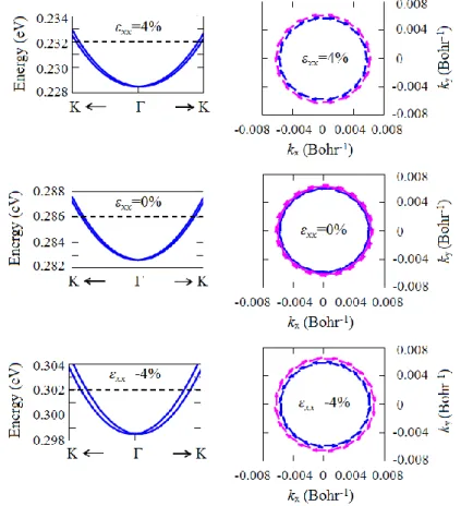
We then investigate the effect of the SOI on strained ZnO. We focused on the SOI on the conduction band minimum (CBM) since n-type ZnO is achieved by introducing Mg doping [27]. As shown in Fig. 2, for the case of unstrained system, very small spin-split bands are identified, which are degenerated at the Γ point because of time reversibility. In these spin-split bands, we find anti-clockwise and clockwise orientation of the Rashba spin rotation for the upper and lower band, respectively. When we introduce biaxial strain, the band splitting substantially enhances. In the case
3
of TBS, the Rashba spin rotations are similar to those of the unstrained system. On the contrary, the direction of Rashba spin rotations becomes opposite in the case of CBS, indicating that the Rashba spin rotations can be inversed by applying biaxial strain.
Figure 2. The spin-split band and spin textures under strain effect. The spin textures are calculated on 3.5 meV above the degenerate state of at CBB
To understand the origin of the inversion of the Rashba spin rotation, we consider the SOI Hamiltonian of the two dimensional free electron system which is expressed as HSOI=αR(kyσx-kxσy), where kx and ky are the wave vectors in the x- and y-directions, respectively, and σx and σy are Pauli matrixes. In this expression, αR is the Rashba spin-orbit strength which is defined as αR =-eħEz/4m2c2, where Ez, m, c, and e are the electric field in the z-directions, theeffective mass, the light velocity, and the elementary charge respectively. When Ez >0, this leads to the fact that the condition of αR >0 is obtained. Therefore, the Rashba spin-rotation are clockwise and anti-clockwise direction for the upper and lower band respectively. On the contrary, opposite Rashba spin rotations are achieved when Ez >
0 since it leads to the case of αR<0.
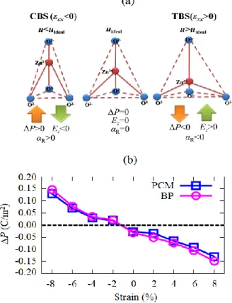
Considering the above arguments and our calculation results of the Rashba spin rotation in Fig. 2, we expect that the negative and positive electric fields Ez are introduced under the CBS and TBS, respectively. These signs of the electric field are consistent with those calculated by using a simple point charge model (PCM) as discussed hereafter. We here consider the PCM including Zn2+
and O2- ions as shown in Fig. 3(a). We evaluate the polarization difference defined as
4
ΔP=P(c/a,u)-P(c/a,uideal), where c/a and u are optimized for a given biaxial strain and uideal = 0.375.
Under substantial CBS, u<uideal [Fig. 3(a)]. Therefore, the PCM leads to the positive ΔP [Fig.3(b)].
This positive value of ΔP is expected to induce the fact that Ez >0. On the contrary, substantial TBS leads to the fact that u>uideal. As a result,the negative ΔP and positive Ez are induced. We therefore conclude that the negative and positive Ez are introduced under CBS and TBS, respectively, and that the directions of the Rashba spin rotations in Fig. 2 are well-explained based on the PCM.
Figure 3. (a) Relation between structural parameter and Rashba spin-orbit strength. (b) The calculated data of the electric polarization different as a function of strain calculated by the PCM and BP methods
To confirm the reliability of the above-mentioned PCM, we here calculate the electric polarization by using Berry phase (BP) method [28,29] [Fig. 3(b)]. In the case of the unstrained system, the value of ΔP calculated from the BP method is -0.031 C/m2, which is very close to the result obtained by using the PCM (-0.0271 C/m2). These values are close to those of past calculations (-0.032 to -0.057 C/m2) [30-31]. When we introduce biaxial strain, we find that our results of ΔP calculated from the PCM are close to those calculated from the BP method, which indicates that the PCM is reliable [Fig. 3(b)].
Here, we present the calculated results of the Rashba spin-orbit strength αR, which is useful for spintronics devices applications. As shown in Fig. 4 that the absolute values of Rashba spin-orbit strength αR enhances under increasing of strain. This indicates that the values of αR can be effectively controlled by tuning the strain. This strain can be achieved by using impurity doping [32] and/or
5
introducing lattice mismatch between ZnO and substrate [33]. Then, our findings of the tunable Rashba effect by applying the biaxial strain are useful to realize spintronics applications of ZnO.
Figure 4. The absolute values of the Rashba spin-orbit strength as a function of strain.
Recently, the quantum well structure of ZnO has been extensively studied [34,35]. Our calculations indicate that two quantum wells consisting of n-type ZnO having opposite directions of the Rashba spin rotations can be realized. By using two quantum wells separated by an energy barrier, an effective spin-filtering due to tunneling is expected to be achieved. In fact, for the spin-filtering device proposed by Koga et. al, two quantum wells having the opposite directions of the Rashba spin rotations were used [36]. Their proposal may give some hint for the device applications of the reversible Rashba effect on ZnO.
Finally, we discuss another possible application of strained ZnO. We find that the Rashba splitting of the unstrained system is small [the absolute values of αR=1.15 meVÅ], which is consistent with the observed long spin relaxation time [37]. In fact, a very small Rashba effect on MgZnO/ZnO interface [αR=0.70 meVÅ] has been experimentally observed [38]. It is expected that the zero (or very small) Rashba splitting can be achieved when we introduce suitable small biaxial strain. When the Rashba effect on ZnO is extremely small, we can achieve a very long spin coherence. Then, ZnO can be used as an efficient spintronics devices.
B. Persistent spin helix on ZnO(10-10) surface
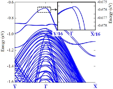
The second part of this dissertation is to study the effect of SOI on the surface system. Here, we consider a surface system oriented on the [10-10] direction. The crystal geometric of the surface and its Brillouin zone are shown in Fig. 5 (a) and (b). Our calculation revealed that occupied surface states appear in band structures in the energy range of -1.3 to -0.65 eV [Fig. 5(c)]. We calculate the partial density of states (PDOS) projected onto the surface atoms [Fig. 5(d)] and find that that the occupied surface state is characterized by O-2p orbitals, which is consistent with the results of past calculations [39]. Given that the surface states are occupied, doping is expected to create a p-type system. Indeed, several studies have succeeded in producing p-type, non-polar wurtzite ZnO films [40,41], giving credence to the notion of creating a p-type wurtzite ZnO(10-10) surface.
The effect of SOC on the surface states can be seen in Fig. 6, wherein the band splitting is small in the Γ-Y direction, but quite large in the Γ-X direction. In these pin-split surface state bands,
6
we find that the spin textures exhibit a quasi-one-dimensional orientation in the inplane y-direction [Fig. 7(a)], yet also have out-of-plane z- components [Fig. 7(b)]. These quasi-one dimensional spin textures are expected to generate current in a direction perpendicular to the spin orientation, as well as induce a greatly enhanced spin relaxation time through the PSH mechanism[13]. This is supported by the fact that a similar PSH has been observed in [110]-oriented zinc-blende QWs with out-of-plane spin orientations [20].
Figure 5. (a) Top view of the crystal geometry of ZnO (10-10) surface. (b) Surface Brillouin zone. (c) Band
structure of ZnO(10-10) surface. The blue and black lines correspond to the band structures of surface and bulk system, respectively. (d) Total and partial density of states projected onto the surface atoms.
To better understand the origin of spin textures, we must consider the SOI of surface states based on group theory[42-44]. This states that the ZnO(10-10) surface belongs to the symmetry point group Cs: the mirror reflections in operation in this symmetry transforms (x,y,z) to (-x,y,z).
Considering the fact that the SOI Hamiltonian is totally symmetric in the Cs point group and includes first-order terms over the wave vectors, SOC can be expressed as HSOI=α1kxσz+α2kxσy+α3kyσx, where α1, α2, and α3 are the spin-orbit strengths. Here, α1 is characterized by the in-plane electric field Ey, whereas α2 and α3 relate to the out-of-plane electric field Ez that originates from the surface effect.
In the case of a bulk system oriented in the [10-10] direction, the out-of-plane electric field Ez vanishes. Consequently, in the kx – ky plane, both α2 and α3 are zero. This leads to a case in which only the first term of HSOI in Eq. (4) remains, meaning that the bands are spin degenerated in the Γ-Y direction and the spin textures are oriented to the out-of-plane z-direction. In surface states, on the other hand, a band split is introduced in the Γ-Y direction due to the third term of HSOI in Eq. (4) [Fig.
7
6]. Furthermore, as a result of the second term in this equation, a tilting of the spin textures in the in-plane y-direction is induced [Fig. 7]. It can therefore be concluded that the above spin-orbit Hamiltonian of the surface state matches well with the calculated results, i.e., the band split in the Γ-Y direction and the tilt of the spin textures.
Figure 6. The spin-split states bands at valence band maximum. The insert shows the spin-split band of the surface states.
Figure 7. (a) The spin textures of the surface state at VBM. The band energy of the spin textures is 1 meV below the highest energy in the occupied surface state. The arrows represent the spin directions projected to the kx-ky plane. (b) Relationships between rotation angle (φk) and spin components.
Since HSOI is strongly affected by the electric field as mentioned above, the origin of the spin textures can be further clarified by studying the electric polarization. On the basis that the spin-split surface state is strongly localized in the first two-bilayers [Fig. 8(a)], the strong electric polarization is expected to occure in these bilayers. To clarify this, the layer-dependence of the electric polarization
8
was calculated using a point charge model (PCM). As shown in Fig. 8(b), this reveals that the strongest electric polarization is identified near the first bilayer.
Electric polarization in the out-of-plane ΔPz and in-plane ΔPy directions was calculated to be 0.077 C/m2 and -0.081 C/m2, respectively. These values indicate that the electric field in the out-of-plane Ez direction is comparable to that in the in-plane Ey direction, which would induce a tilting of the spin orientation [Fig. 8(c)]. However, only the in-plane electric polarization is observed in the case of bulk system [ΔPy-bulk= -0.027 C/m2 ]. This leads to the fact that the in-plane elctric field Ey is generated, but induces a spin orientation with a fully out-of-plane z-direction [Fig. 8(d)]. This would confirm that the spin textures in Fig. 7 are well-consistent with the PCM results.
Figure 8. (a) Expected values of spin projected to the atoms in each bilayers. The calculations are performed in
the surface state in Fig. 7(a). The top of the surface is represented by N=1. (b) Calculated data on the in-plane and out-of-plane electric polarizations in each bilayers using PCM. Schematic view of the spin textures and electric fields for the case of the surface (c) and bulk systems (d).
Recently, PSH that induces a greatly enhanced spin relaxation time has been extensively studied [13-20], with our calculations indicating that this is in fact achieved using the ZnO(10-10) surface. Since the calculated results of spin textures show a quasi-one-dimensional orientation, this inhibits the precession of the spins, thereby increasing the spin relaxation time. A similar mechanism behind long spin relaxation times has been reported in [110]-oriented zinc-blende QWs [45-47], suggesting that the ZnO(10-10) surface could provide an efficient spintronics device.
The spin-orbit strength of the PSH (αPSH), a variable of interest in spintronics device applications, was calculated using the band dispersion in Fig. 2. This found that the value of αPSH is
9
quite substantial (34.78 meVÅ) and much larger than what has been observed in the PSH of various zinc-blende n-type QW structures of GaAs/AlGaAs [3.5 to 4.9 meVÅ) [15], 2.77 meVÅ [19]] and InAlAs/InGaAs [1.0 meVÅ [17], 2.0 meV˚A [18]]. This large value of αPSH should ensure a small wavelength of PSH (λPSH), which is important to the miniaturization of spintronics devices. As it happens, the calculated value λPSH (0.19 μm) was in fact one-order less than that observed in the direct mapping of PSH (7.3 to 10 μm [15]) and the resonant inelastic light-scattering measurement (5.5 μm [19]) of GaAs/AlGaAs QWs.
III. Conclussion
We have systematically studied the effect of SOI on ZnO by using first-principles DFT calculations. For the case of the strained bulk system, we revealed that the SOI shows the Rashba type.
We found that the Rashba spin rotation can be inversed by applying biaxial strain. Furthermore, we revealed that the Rashba spin-orbit strength can be effectively controlled by tuning the strain, suggesting that the strained bulk system is suitable for spintronics applications.
In the case of surface system, on the other hand, we found that the SOI leads to the persistent spin helix (PSH), exhibiting a quasi-one dimensional orientation of the spin textures. This particular of PSH is expected to induce the long spin lifetime, which is important to realize energy-saving spintronics devices. Furthermore, we revealed that the wavelength of this PSH is smaller than that observed with various zinc-blende quantum well structures, suggesting that the present system enables for the miniaturization of the spintronics devices.
Finally, we conclude that both the strained bulk and the surface system are promising for spintronics applications.
Bibliography
[1] I. Zutic, J. Fabian, and S. D. Sarma, Rev. Mod. Phys. 76, 323 (2004).
[2] A. Hirohata and K. Takanashi, J. Ohys. D, Apl. Phys. 47, 193001 (2014).
[3] M. N. Baibich et. al., Phys. Rev. Lett. 61, 2472 (1988).
[4] G. Binasch et. al., Phys. Rev. B 39, 4828 (1989).
[5] R. Fiederling et. al., Nature 402, 787 (1999).
[6] H. Ohno et. al., Nature 408, 944 (2000).
[7] M. Tanaka and Y. Higo, Phys. Rev. Lett. 87, 026602 (2001).
[8] S. Mishra, G. S. Tripathi, and S. Satpathi, Phys. Rev. B 77, 125216 (2008).
[9] Y. A. Bychkov and E. I. Rashba: J. Phys. C 17, 6039 (1984).
[10] S. Datta and B. Das: Appl. Phys. Lett. 56, 665 (1990).
[11] S. Kuhlen, et. al., Phys. Rev. Lett. 109, 146603 (2012).
[12] X.-L. Qi, Y.-S. Wu, and S.-C. Zhang, Phys. Rev. B 74, 085308 (2006).
[13] B. A. Bernevig, J. Orenstein, and S.-C. Zhang, Phys. Rev. Lett. 97, 236601 (2006).
[14] J. D. Koralek, et. al., Nature 458, 610 (2009).
10
[15] M. P. Walser, C. Reichl, W. Wegscheider, and G. Salis, Nat. Phys. 8, 757 (2012).
[16] M. Kohda, et. al., Phys. Rev. B 86, 081306 (2012).
[17] J. Ishihara, Y. Ohno, and H. Ohno, Applied Physics Express 7, 013001 (2014).
[18] A. Sasaki, et. al., Nat. Nano. 9, 703 (2014).
[19] C. Schonhuber, et. al., Phys. Rev. B 89, 085406 (2014).
[20] Y. S. Chen, S. Falt, W. Wegscheider, and G. Salis, Phys. Rev. B 90, 121304(2014).
[21] A. Tsukazaki, et. al., Science 315, 1388 (2007).
[22] A. Tsukazaki, et. al., Nat. Mater. 9, 889 (2010).
[23] J. Ye et. al., Sci. Rep. 2, 533, (2012).
[24] K. Han, et. al., Appl. Phys. Lett. 100, 192105 (2012).
[25] S. Ghosh, V. Sih, W. H. Lau, and D. D. Awschalom, Appl. Phys. Lett. 86, 232507 (2005).
[26] T. Ozaki, H. Kino, J. Yu, M. J. Han, N. Kobayashi, M. Ohfuti, F. Ishii, T. Ohwaki, H. Weng, M. Toyoda, and K. Terakura: http://www.openmxsquare.org/
[27] R. Dutta and N. Mandal: Appl. Phys. Lett. 101 (2012) 042106.
[28] R. D. King-Smith and D. Vanderbilt: Phys. Rev. B 47 (1993) 1651.
[29] R. Resta: Rev. Mod. Phys. 66, 889 (1994).
[30] A. Malashevich and D. Vanderbilt: Phys. Rev. B 75, 045106 (2007).
[31] A. D. Corso, M. Posternak, R. Resta, and A. Baldareschi, Phys. Rev. B 50, 10715 (1994).
[32] H. Matsui and H. Tabata: J. Appl. Phys. 113, 183525 (2013).
[33] R. Ghosh, D. Basak, and S. Fujihara: J. Appl. Phys. 96, 2689 (2004).
[34] P. Pant, J. D. Budai, and J. Narayan: Acta Mater. 58, (2010) 1097.
[35] M. Al-suleiman et al., Appl. Phys. Lett. 91 (2007) 081977.
[36] T. Koga, J. Nitta, H. Takayanagi, and S. Datta, Phys. Rev. Lett. 88, 126601 (2002).
[37] S. Ghosh, V. Sih, W. H. Lau, and D. D. Awschalom, Appl. Phys. Lett. 86. 232507 (2005).
[38] Y. Kozuka, S. Teraoka, J. Falson, A. Oiwa, A. Tsukazaki, S. Tarucha, and M.
Kawasaki, Phys. Rev. B 87, 205411 (2013).
[49] H. H. Zhang, et. al., App. Phys. Lett. 104, 112106 (2014).
[40] P. Schroer, P. Kruger, and J. Pollmann, Phys. Rev. B 49, 17092 (1994).
[41] P. Ding, et. al., J. Cryst. Growth 331, 15 (2011).
[42] T. Oguchi and T. Shishidou, J. Phys. Cond. Matt. 21, 092001 (2009).
[43] E. Simon, et. a, Phys. Rev. B 81, 235438 (2010).
[44] S. Vajna, et. al., Phys. Rev. B 85, 075404 (2012).
[45] S. Dohrmann, et. al., Phys. Rev. Lett. 93, 147405 (2004).
[46] O. D. D. Couto, et. al., Phys. Rev.Lett. 8, 036603 (2007).
[47] Y. Ohno, et al., Phys. Rev. Lett. 83, 4196 (1999).