九州大学学術情報リポジトリ
Kyushu University Institutional Repository
フレキシブル有機熱電変換素子の実用化に向けて
黄, 善彬
https://doi.org/10.15017/1806988
出版情報:Kyushu University, 2016, 博士(工学), 課程博士 バージョン:
権利関係:Fulltext available.
1
Toward the Practical-Use of
Flexible Organic Thermoelectric Generators
A Dissertation Presented to the Academic Faculty
By
SUNBIN HWANG
In Partial Fulfillment
Of the Requirements for the Degree Doctor of Philosophy in Engineering
Department of Chemistry and Biochemistry Graduate School of Engineering
Kyushu University
March 2017
2
Table of Contents
CHAPTER 1 Introduction to organic thermoelectric generators ... 5
1.1 Thermoelectric generators ... 6
1.2 Physics of thermoelectric generator ... 8
1.2.1 Thermoelectric (Seebeck) effect ... 8
1.2.2 Thermal conduction and Joule heating ... 10
1.2.3 Thermoelectric figure of merit (𝒁) and power conversion efficiency (𝜼) ... 11
1.3 Organic thermoelectric generators ... 13
1.3.1 General thermoelectric materials ... 13
1.3.2 Organic thermoelectric materials ... 14
1.3.3 Doping of organic materials ... 15
1.3.4 Existing processes and challenges for making organic thermoelectric modules . 19 1.3.5 State-of-the-art and challenges for OTEGs ... 21
1.4 Goal of the dissertation ... 25
CHAPTER 2 Processing and doping of thick polymer active layers for flexible organic thermoelectric modules... 26
2.1 Introduction ... 27
2.2 Experimental ... 30
2.3 Results and Discussion ... 32
2.3.1 Effect of doping on thermoelectric properties ... 32
2.3.2 Morphology ... 34
2.3.3 Air stability ... 36
2.3.4 Solution-processed modules ... 38
2.3.5 Module doping concentration optimization ... 41
2.3.6 Analysis of module design ... 43
2.4 Conclusions ... 45
CHAPTER 3 Solution-processed organic thermoelectric material exhibiting doping- concentration-dependent polarity ... 46
3.1 Introduction ... 47
3.2 Experimental ... 49
3.2.1 Device fabrication ... 49
3.2.2 Thermoelectric properties ... 49
3.2.3 UPS and XPS measurements ... 50
3.2.4 Other measurements ... 50
3.3 Results and discussion ... 51
3
3.3.1 Effect of doping on thermoelectric properties ... 51
3.3.2 Doping mechanism between P(PymPh) and NaNap ... 53
3.3.3 Thermoelectric properties ... 54
3.3.4 Temperature dependence of thermoelectric properties ... 56
3.3.5 Analysis of electronic structure ... 58
3.3.6 Mechanism of doping-concentration-dependent polarity ... 60
3.4 Conclusions ... 63
CHAPTER 4 Interplay among thermoelectric properties, atmospheric stability, and electronic structures in solution-deposited thin films of poly (nickel 1,1,2,2-ethenetetrathiolate)64 4.1 Introduction ... 65
4.2 Experiment ... 67
4.2.1 Device fabrication ... 67
4.2.2 Thermoelectric properties ... 67
4.2.3 UPS and XPS measurements ... 68
4.2.4 Other measurements ... 68
4.3 Results and discussion ... 69
4.3.1. Thin-film fabrication process and morphology ... 69
4.3.2. Qualitative analysis ... 70
4.3.2. Effect of dehydration on the electronic states ... 72
4.3.3. Effect of dehydration on thermoelectric properties ... 74
4.3.4. Air stability ... 75
4.4 Conclusions ... 79
CHAPTER 5 Results and discussion ... 80
5.1 Summary of the dissertation ... 81
5.2 Future strategy ... 82
Appendix A ... 87
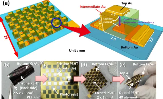
A-1 Fabrication of P3HT nano- and micro-films ... 87
A-2 Patterning by photo-etching process ... 88
A-3 Changes of doped state of P3HT and stability of electrical conductivity in air condition ... 89
A-4 Thermoelectric performance of recycled P3HT ... 90
A-5 Thermoelectric measurement system for flexible thermoelectric modules ... 91
Appendix B ... 92
B-1 Synthesis ... 92
B-2 Measurement of Seebeck coefficient of single OTEGs... 94
4
B-3 Comparison between DMBI and NaNap as electron donors... 97
B-4 XPS ... 98
B-5 Thermally stimulated doping of P(PymPh) ... 98
B-6 TG-DTA measurement ... 99
B-7 XRD ... 100
B-8 Hall measurement ... 101
B-9 Morphology ... 103
B-10 Picture of measurement system ... 103
Appendix C ... 104
C-1 Solution processed P(NaX[Niett]) gel and net ... 104
C-2 XPS ... 105
C-3 TG-DTA measurement ... 106
C-4 UPS ... 107
References ... 108
List of Tables ... 119
List of Figures ... 120
List of Symbols and Abbreviations ... 126
Publication list ... 130
List of presentations at international conferences ... 131
Acknowledgments ... 132
5
CHAPTER 1
Introduction to organic thermoelectric generators
6
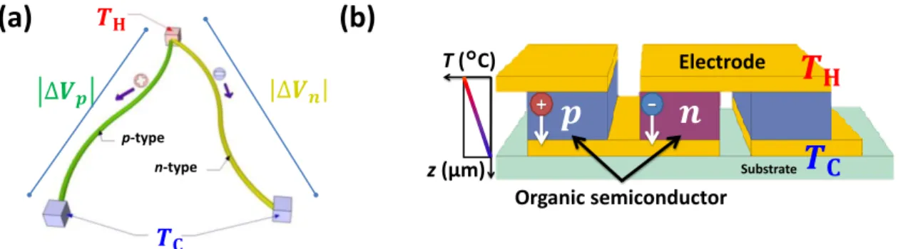
1.1 Thermoelectric generators
Figure 1.1: Practical examples and the typical π-leg type structure of flexible organic thermoelectric generators.
Electronic devices have become an indispensable tool for modern society as their presence continues to grow. To continue the rapid development of information technology and the spread of mobile electronics, power source and consumption issues must be addressed. Currently, the development and dissemination of high-performance batteries is progressing, but there are still various performance problems and limitations that inhibit the further development and proliferation of electronics. Energy harvesting technologies that can collect unused energy that exists around us (e.g., solar, vibration, heat and wind) have been targeted as a key strategy to solve these power supply problems.1–4
Thermoelectric energy conversion is one attractive possible solution as it offers an extremely reliable and silent power source with no moving parts. Furthermore, electricity can be generated from the waste heat produced by things such as power plants and machinery even at low temperatures because only a small temperature difference is required across a thermoelectric generator (TEG). However, if TEGs are too bulky, heavy, or rigid, the number of existing industrial and natural environments to which they can be easily adapted will be limited. Additionally, although the thermoelectric effect driving the devices has been known for nearly two centuries, growth of the inorganic TEG industry has been limited because of very low efficiencies and high production costs.5
Organic thermoelectric generators (OTEGs) replace the traditional inorganic active materials in TEGs with organic compounds and have additional advantages such as low
Sensor
Automobile Electricity
Daimler & BASF Germany
Fujitsu laboratories ltd Japan
Engine Plant & factory
Solar heat
Body heat
T (°C)
z (μm) Substrate
Electrode
Organic semiconductor
7
thermal conductivity, light weight and flexibility. Such properties give OTEGs the potential to be used to easily cover large heat-exchanger surfaces of any shape and size. Organic materials also offer the prospect of low-temperature solution processing, which could enable the roll- to-roll mass printing of large-area, integrated modules and reduce costs.6 Therefore, as shown in Fig. 1.1, OTEGs could become the most versatile distributed power generation technology in the near future with applications from wearable electronics to power supplies for mobile devices and distributed sensor networks.2
8
1.2 Physics of thermoelectric generator 1.2.1 Thermoelectric (Seebeck) effect
A temperature difference between two points in a conductor or semiconductor results in an electromotive force between these two points. In other words, a temperature gradient in a conductor or a semiconductor generates a built-in electric field. This phenomenon, which was discovered by Estonian-German physicist Thomas Johann Seebeck in 1820, is referred to as the Seebeck effect or the thermoelectric effect and makes possible the conversion of heat to electricity.7 The Seebeck coefficient (𝑺) is a measure of the magnitude of this effect and is defined as the thermo-electromotive force (thermoelectric voltage, ∆𝑽𝐓𝐄) produced per unit Kelvin of temperature gradient (∆𝑻) applied across a conductor or semiconductor (Eq 1.1).
𝑺 = 𝐥𝐢𝐦
∆𝑻→𝟎
∆𝑽𝐓𝐄
∆𝑻 =𝐝𝑽𝐓𝐄
𝐝𝑻 . (Equation 1.1)
Figure 1.2: Effect of a temperature gradient on the charge carrier diffusion in a single conductor and change of potential.
The physical mechanism driving the Seebeck effect is shown in Fig. 1.2 and can be understood as follows. Charge carriers available for conduction in the material under the influence of a temperature gradient start to diffuse from the high temperature region, where the carriers have higher energy, to the low temperature region. This process continues until steady state is reached. Steady state is characterized by a stable Seebeck voltage, which arises as a force to act against the further migration of charge carriers.
Considering the case of open circuit in a p-type element with more holes than electrons, thermally excited holes on the hot side will have excess energy and diffuse to the low- temperature side. On the other hand, high energy electrons in the conduction band of the hot side of an n-type element with an excess of electrons will diffuse to the low-temperature side.
As a result, ionized acceptors, which are negatively charged, remain on the hot side of the p- type element, and the cold side is positively charged. Conversely, positively charged donors remain on the high temperature side of an n-type element, and the cold side is negatively
E
0 1 F(E)
EF QC
E
0 1 F(E) EF
QH
− −
− −
+ + + +
ΔVTE
9
charged. Thus, the Seebeck coefficient is positive if the majority of charge carriers are holes, whereas it is negative when the majority carriers are electrons.
As holes or electrons accumulate on the cold side, an electric field is produced that induces a current in the direction opposite to that of the carriers under the temperature gradient. Steady state is reached when the temperature-driven current and field-induced current balance to zero, resulting in the open-circuit voltage. Temperature can be measured from the voltage across two terminals of a thermocouple that are at the same temperature by using the fact that the Seebeck coefficients of n-type and p-type material are different.
Figure 1.3: (a) Seebeck effect illustrated in a circuit comprising two dissimilar materials. (b) π-leg type thermocouple for power generation based on the Seebeck effect.
For example, Fig 1.3a shows a standard thermocouple configuration consisting of two dissimilar materials connected to form a circuit. When the junction is heated to a temperature 𝑻𝐇 and the reference points held at a cooled temperature 𝑻𝐂 to create a temperature gradient (𝚫𝑻 = 𝑻𝐇 − 𝑻𝐂), an electromotive force (thermoelectric voltage) is induced that can be expressed as
Δ𝑉TE,Total = Δ𝑉TE,𝑝− Δ𝑉TE,𝑛 = ∫TTH𝑆𝑝(𝑇) − 𝑆𝑛(𝑇)
C . (Equation 1. 2)
In a junction between two dissimilar materials like Fig. 1.3a, charge carriers of each conductor with higher electronic pressure will tend to diffuse into a lower pressure region of the other conductor and once again the thermoelectric voltage will build up. This voltage difference is of course dependent on a material type (n- or p-type) and temperature gradient.
At higher temperature, the charge carriers’ velocity is substantially increased, which corresponds to a greater “electronic pressure.” In this situation, the voltage difference measured in a circuit will be further increased. As it is seen from Eq. 1.2, one needs to use two conductors with Seebeck coefficients having opposite signs to acquire high ∆𝑽𝐓𝐄. Based on this principle, thermocouples consisting of p- and n-type semiconductors that have known
T (°C)
z (μm) Substrate
Electrode
Organic semiconductor
(a) (b)
n-type p-type
10
Seebeck coefficients are often used as temperature sensors. A similar structure can be used for power generator by modifying the configuration and connecting a large number of p- and n-elements to further increase the output voltage (Fig. 1.2b).
Direct measurement of the absolute Seebeck coefficient of a conductor is not possible because contacts, which will almost certainly have different properties than the material being studied, must be made to the sample to measure the voltage. Even if contacts can be made from the same material as the sample, the internal electrodes of the measurement system will be at the same temperature, so no net thermoelectric voltage can be measured. For that reason, the combination of two different materials is always used in Seebeck coefficient measurements. Individual coefficients can be calculated if, at a given ∆𝑻, the Seebeck coefficient of one of the materials (e.g., a reference such as Platinum) forming the thermocouple is known with good precision or negligibly small compared to the second material.8
1.2.2 Thermal conduction and Joule heating
The thermoelectric effect is accompanied by two irreversible processes, Joule heating and thermal-heat conduction, that always tend to lower the thermoelectric device performance.
Their presence prevents device efficiency from attaining its thermodynamic limit, better known as the Carnot efficiency.
Joule heating inevitably occurs as a consequence of any electric current and, in the case of thermoelectrics, is particularly undesirable as it converts useful electric energy into heat that is dissipated, resulting in a so-called ohmic loss. The amount of Joule heating is a function of electrical current (𝑰) and resistivity (𝑹), as shown in Eq. 1.3.
𝐼2𝑅 (Equation 1.3) Joule heating
Figure 1.4: (a) The heat conduction in a plate-shaped solid layer. (b) p-type and (c) n-type operation modes of thermoelectric elements.
Temperature (K)
Thickness (m)
p-type
n-type
(a) (b)
(c)
11
In a conductor subject to a temperature gradient, an increase in the temperature of its cold side is always observed as a result of heat conduction. The quantity of heat flow (𝑸) across a temperature gradient can be expressed by Fourier’s law as
𝑄 = −𝐴𝜅d𝑇
d𝑡, (Equation 1.4) Fourier's law
where 𝑨 is the cross-section area of the conductor, 𝜿 is the material’s thermal conductivity, 𝑻 is the temperature gradient as function of thickness, and 𝒕 is the thickness of the conductor, as shown in Fig. 1.4a. The thermoelectric efficiency loss caused by heat conduction is directly proportional to 𝜿; hence, materials with low thermal conductivity are required for efficient energy conversion.
1.2.3 Thermoelectric figure of merit (𝒁) and power conversion efficiency (𝜼)
Next, the power conversion efficiency of thermoelectric elements based on the aforementioned equations will be discussed. Consider power-generating thermoelectric elements placed under a temperature gradient (𝑻𝐇 and 𝑻𝐂 at each ends), as shown in Fig.
1.4b and c. In the following, it is assumed that the temperature difference (∆𝑻 = 𝑻𝐇− 𝑻𝐂) is small and the transport coefficients (𝑺𝒙, 𝝈𝒙, 𝜿𝒙) do not depend on the temperature. If the thermal power flowing into the hot side of the element and out of the cold side of the element are defined as 𝑸𝐇 and 𝑸𝐂, respectively, the decrease in thermal power (∆𝑸 = 𝑸𝐇− 𝑸𝐂) is the portion converted into electricity. Thus, the thermoelectric conversion efficiency can be defined as the ratio ∆𝑸/𝑸𝐇. The incoming thermal power at the hot side of the element and the decrease of thermal power can be expressed by Eq. 1.5 and Eq. 1.6, respectively.7
𝑄H = 𝜅𝑥∆𝑇 + 𝑆𝑥𝐼𝑇H−1
2𝐼2𝑅 (𝑥 = 𝑝 or 𝑛) (Equation 1.5)
∆𝑄 = 𝐼2𝑅 + 𝑆x𝐼∆𝑇 (Equation 1.6)
From Eqs. 1.5 and 1.6, conversion efficiency can then be expressed as
𝜂 = ∆𝑄
𝑄H = 𝐼2𝑅+𝑆𝑥𝐼∆𝑇
𝜅𝑥∆𝑇+𝑆𝑥𝐼𝑇H−1
2𝐼2𝑅 . (Equation 1.7)
On the base of the temperature gradient distribution, the electric current at the maximum thermoelectric power conversion efficiency (Eq. 1.7) should satisfy 𝝏𝜼/𝝏𝑰 = 𝟎.
12
The electric current that satisfies this condition is given by 𝑰 =𝜿𝒙∆𝑻
𝑺𝒙𝑻̅ (√𝟏 + 𝒁𝑻̅ − 𝟏), and the maximum thermoelectric power conversion efficiency (𝜼𝐌𝐚𝐱) can then be defined by the following equation.
𝜂Max=Δ𝑇
𝑇H
√1+𝑍𝑇̅−1
√1+𝑍𝑇̅+𝑇C 𝑇H
(𝑇̅ =𝑇H+𝑇C
2 , 𝑍 =𝜎𝑆𝑥2
𝜅𝑥 ) (Equation 1.8)
The first term of this equation (𝚫𝑻/𝑻𝐇) is the Carnot efficiency, which 𝜼𝑴𝒂𝒙 cannot exceed.
The relationship between 𝜼𝑴𝒂𝒙 and 𝒁𝑻̅ for different temperature gradients is shown in Fig 1.5. From these graphs, 𝜼𝑴𝒂𝒙 is shown to be a monotonically increasing function of 𝒁𝑻̅. Thus, 𝒁𝑻̅ is a key figure to evaluate performance and is called the dimensionless thermoelectric figure of merit, which consists of the figure of merit (𝒁) and the average of the temperatures on the two sides of the device (𝑻̅).
Figure 1.5: Relationship of 𝒁𝑻̅ and maximum thermoelectric power conversion efficiency (𝜼𝑴𝒂𝒙) for various 𝚫𝑻 with the temperature of the cold side 𝑻𝐂 maintained at 0 °C (273.15 K).
0.0 0.5 1.0 1.5 2.0
0 2 4 6 8 10
Max (%)
ZT (-)
T = 20 °C T = 40 °C T = 60 °C T = 80 °C T =100 °C
TC = 0 °C
(-)
13
1.3 Organic thermoelectric generators 1.3.1 General thermoelectric materials
According to the definition of 𝒁𝑻̅ in Fig 1.6a, where the thermal conductivity 𝜿 is the sum of a carrier component (𝜿𝐞𝐥) and a lattice (phonon) component (𝜿𝐩𝐡), a high electrical conductivity (𝝈) and high Seebeck coefficient (𝑺) are required while maintaining a low thermal conductivity to obtain high performance thermoelectric materials.7,9–11 These factors are all a function of free carrier concentration as shown in Fig 1.6b.
Figure 1.6: (a) Factors influencing the performance of thermoelectric device. (b) Seebeck coefficient and electrical and thermal conductivity as a function of free carrier concentration.
Heavily doped semiconductors can have high electrical conductivities that approach those of metals, but the Seebeck coefficients of heavily doped semiconductors are usually very low. In general, carriers with energy above the Fermi level tend to increase the Seebeck coefficient, and those with lower energies contribute to making it smaller. Consequently, in metals that typically have half-filled bands, the thermopower is relatively small. The resulting thermoelectric efficiency is further decreased by high thermal conductivities. Likewise, low- doped inorganic semiconductors with their extremely large Seebeck coefficient (up to several mV K−1) and some of the lowest thermal conductivities (less than 1 W m−1 K−1) of known materials are equally unfit for thermoelectric applications due to poor electrical conduction.
Thus, controlling the carrier density in the active materials is important for optimizing performance in thermoelectric devices.
Because quantum effects, which can reduce the high lattice thermal conductivity (𝜿𝐩𝐡) of an inorganic material by inducing phonon drag with superlattices and quantum wells, in inorganic thermoelectrics can be used to achieve good thermoelectric materials, the search for efficient thermoelectric materials has accelerated again in recent year. The list of
Optimum doping level
Seebeckcoefficient σ(S cm−1)
κel
Carrier density
1017 1018 1019 1020 1021
|S| (μVK−1) Electric Conductivity
p or n (cm−3)
|S| σ
S2σ
Power Factor
Thermal conductivityκ(W m−1 K−1)
κph κ = κel+ κph
Electron Lattice
TE figure of merit (-)
Seebeck coefficient (μV K−1)
Conductivity (S cm−1)
Thermal Conductivity (W m−1K−1)
(a) (b)
14
candidates is long and plentiful. Among them, some of the most studied thermoelectrics are Bismuth chalcogenides, inorganic clathrates, Half Heusler alloys, skutterudite materials, silicides, and oxides.12–14
1.3.2 Organic thermoelectric materials
Figure 1.7: (a) sp2 hybridization in π-conjugated system where electron density can be delocalized over many carbon atoms. (b) An example where the metal center donates electrons through a d orbital to the ligand's empty orbital (d-π conjugated system).
The majority of organic thermoelectric materials in the literature are based on π- conjugated polymers. Such π-conjugated (see Fig 1.7a) organic conducting polymers represent a rather overlooked class of thermoelectrics that is nonetheless suitable for room temperature energy conversion.10,15 Their generally low thermal conductivities and satisfactory Seebeck coefficients and electrical conductivities are not the only reason they are being considered for low temperature thermoelectric generation. Organic semiconductor materials have potential advantages of a wide range of form factors, reduced production cost, nontoxicity, no reliance on rare metals, and abundance.
Many π-conjugated polymers have already been tested in the search for thermoelectric materials that have great potential. For example, polyaniline (PANI), polythiophene (PTH), poly(3,4-ethylenedioxythiophene):poly(styrenesulfonate) (PEDOT:PSS), polyacetylene (PA), polypyrrole (PPy), polycarbazoles (PC), polyphenylenevinylene (PPV), and their derivatives show promise and are certainly worth further investigation for p-type thermoelectric materials.16 Polymers consisting of electronic acceptor units such as pyridine (Py), naphthalene diimide (NDI), diketopyrrolopyrrole (DPP), benzodifurandione (BDF), benzobisthiadiazole (BBT), and their derivatives have also been investigated as n-type thermoelectric materials.17–26 In particular, recent progress using poly(3,4- ethylenedioxythiophene):iron(III) p-toluenesulfonate (PEDOT:Fe3+-tos3) has yielded remarkably high performance comparable to that of inorganic materials.11
Recently, d-π conjugated (See Fig 1.2b) metallo-organic complexes with nickel and copper as the metal centers have attracted attention because of their high electrical conductivities. A conducting metallopolymer called a metal-organic-framework (MOF) can be chemically
2p orbital (filled) 3d orbital
(empty)
(b) (a)
15
prepared through the reaction of ethenetetrathiolate with metal halide to give an insoluble, amorphous polymer. These MOFs can be either linear or two- or three-dimensional and can be obtained with a wide range of physical and electronic properties.11 In particular, poly(metal 1,1,2,2-ethenetetrathiolate) P(Mett) based MOFs have yielded remarkably high performance as stable n-type thermoelectric materials.11
1.3.3 Doping of organic materials
The presence of a π-π and/or d-π conjugated chain is the first fundamental requirement for a polymer to become conducting. However, the band gaps of conjugated polymers generally range from 1 to 3 eV,27 which is consistent with semiconducting or even insulating properties. To obtain high electrical conductivity, a doping process is used. In contrast to inorganic doping processes involving the replacement of atoms, doping in conducting polymers is due to an oxidation (p-type doping) or reduction (n-type doping) process. The oxidation level in conducting polymers can be extremely high, sometimes up to 50%,28 exceeding that of inorganics by several orders of magnitude. Oxidation/reduction can be achieved by removing/adding an electron from/to a polymer via an electron transfer (i.e., charge transfer) reaction with a chemical species (chemical redox reaction) or with an electrode (electrochemical reaction). The doping charge on the polymer is stabilized by a counter ion (cation/anion) to ensure electroneutrality of the materials. Polymers can also be synthesized either in a doped state or a neutral state.
The oxidation level can be controlled in a number of ways. Chemical doping is a method that involves the exposure of a polymer to a solution or vapor that contains the dopant.29 Throughout the doping process, chemical dopants can physically penetrate into or move out of the polymer, putting a strain on the polymer film that can cause swelling, shrinking, or other morphological changes. An increase in the charge carrier concentration by doping results in a change in electrical conductivity, which can lead to conductivities similar to metals in some highly ordered polymers.30
The redox potential, ionization potential, and electron affinity of the dopant and polymer must be considered when searching for a good dopant/polymer pair. The ionization potential of a material is related to the electrochemically measured oxidation potential and can be correlated to the energy of its highest occupied molecular orbital (HOMO). The electron affinity, which is related to the electrochemical reduction potential, can be correlated to the lowest unoccupied molecular orbital (LUMO).31–33
16
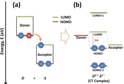
Figure 1.8: Schematic of (a) the charge transfer from donor to acceptor and (b) the formation of new effective energy levels.
For charge transfer to occur and create additional carriers, the HOMO of the donor and LUMO of the acceptor should be aligned so that an electron can transfer from the donor to acceptor, as shown in Fig 1.8a. If the dopant acts as acceptor, then excess holes are created on the semiconductor polymer; for a dopant that is a donor, excess electrons are created.
When a donor and acceptor with the necessary properties for charge transfer are adjacent, an intermolecular complex called a charge-transfer (CT) complex can be formed.
One characteristic of CT complexes is that they can form their own effective ground and excited state levels that can absorb light, as shown in Fig 1.8b.34,35 As a consequence, the HOMO (donor)–LUMO (acceptor) energy difference can sometimes determine the lowest energy electronic transition in the UV-vis spectrum of the charge-transfer complex formed by the same species according to Eq. 1.9.36
𝒉𝝂 = 𝑰𝑷𝐃− 𝑬𝑨𝐀− 𝑲(𝑫𝜸+𝑨𝜸−) ~ 𝑬𝑨𝒄𝒄𝒆𝒑𝒕𝒐𝒓𝟎 −𝑬𝑫𝒐𝒏𝒐𝒓𝟎 (Equation 1.9)
Here, 𝒉𝝂 is the absorption energy of the non-ionic ground state of the CT complex (i.e., neutral CT complex), 𝑰𝑷𝐃 and 𝑬𝑨𝐀 are the ionization potential of the donor and electron affinity of the acceptor, respectively, and 𝑲(𝑫𝛄+𝑨𝛄−) is the electrostatic energy between the donor and acceptor. 𝜸(≥ 𝟎) is the amount of charge transfer (𝜸 = 1 is ionic and 𝜸 = 0 is a neutral CT complex). 𝑬𝐃𝐨𝐧𝐨𝐫𝟎 and 𝑬𝐀𝐜𝐜𝐞𝐩𝐭𝐨𝐫𝟎 are standard reduction potentials of the donor and acceptor, respectively.
For example, if the polymer being doped is an electron donor and the dopant is an acceptor, the HOMO of the polymer and the LUMO of the dopant should be similar for charge transfer to occur. For any host and dopant combination, confirming whether free carriers are
(a)
Acceptor
Donor
Acceptor
− −
LUMO HOMO
Energy, E (eV)
+ Donor
−
−
−
−
(CT Complex)
−
−
LUMO+1
LUMO
HOMO
HOMO-1
(b)
17
generated by the doping process is very important. Based on the previous description, UV- Vis-NIR absorption spectroscopy is an effective method to confirm the CT between polymer and dopants.
Figure 1.9: General electronic structures of (a) n- and (b) p-type polymer chains having quinoid resonance at various reduction (left to right) and oxidation (right to left) states respectively.7,37 The transitions of these species are labeled with Roman numerals corresponding to features in (c). (c) The general optical spectra of these species.
Most conjugated polymers have a non-degenerate ground state, which impedes soliton formation. Polarons and bipolarons in such polymers are suggested to be created upon doping (see Fig.1.9a and b).38 The reduction or oxidation of the polymer leads to the formation of a radical anion or cation, respectively. Their presence causes an attenuation of neighboring bond alteration amplitudes and the formation of sub-electronic levels between the conduction and valence bands. A polaron is a single charge excitation that can be either positive when an electron is removed from a polymer chain or negative in the case when an
Intensity (a.u.)
Energy (eV)
0.0 0.5 1.0 1.5 2.0 2.5 2500 1250 800 620 500Wavelength (nm)
I
II III
IV Polaron
(n−) Neutral
n-type
High doping level (metallic-like electric properties)
Bipolaron (n− −) III
Neutral p-type
Non-doping level Non-doping level
Polaron (p+) Bipolaron
(p+ +)
e- e- e- e-
EF
(a)
(c)
(b)
I I
III
II IV II
IV
V
18
electron is added to a polymer chain. The distortion caused by a polaron can spread over three to four monomers depending on the polymer’s chemical structure. Removal/addition of an electron from a polaron produces a bipolaron (i.e., a radical ion pair) associated with a strong local lattice distortion.39
This unique energy structure of the film and the charge carrier affects the optical properties. The evolution of the optical properties of a conjugated polymer subject to doping is illustrated in Fig. 1.9c.
A neutral polymer chain of planar symmetry displays a first optical transition from the top of the valence band to the bottom of the conduction band (transition I). The absorption feature is associated with a transition between the HOMO–LUMO of the neutral polymer.
Upon doping, new polaronic or bipolaronic states appear in the band gap of the polymer. Due to the planar symmetry of a polymer chain, these intra-band gap states manifest themselves as new optical transitions (transitions II and III in the case of a radical-cation or radical-anion (polaron) and a single transition IV in the case of a dication or dianion (bipolaron) on a polymer chain).
In the solid state, the aggregated polymer chains make more transitions possible.40 With additional shifting and broadening effects, strictly identifying transitions for polarons and bipolarons becomes difficult. The situation is also complicated at high doping levels, but a (bi)polaron band typically exhibits a broad IR absorption eventually extending in the far IR.41
Though doping is necessary to increase carrier concentration, the choice of chemical dopants is rather limited since the requirements for a dopant are affected by the unique polymer electronic structure on a case-by-case basis. Moreover, there are some known downsides to this approach, such as chemical stability issues of the dopants due to their high reactivity. Another problem arises from the difficulty of maintaining the doped samples in the initial doped state. Because of this, a conductive polymer that is initially in a heavily doped state may fail to sustain its doped state and high conductivity.42 For thermoelectric devices, maintaining and controlling the doped state is crucial since the thermoelectric properties will change with the doped state. An alternative method that overcomes some of these problems is electrochemical doping.
In electrochemical doping, an electrolyte is used between a conducting polymer and an electrode that supplies the charge to the polymer when a potential is applied between the polymer and electrode. Ions from the electrolyte diffuse in and out of the polymer to maintain its charge neutrality. In the case of n-doping, the polymer is reduced and cations from the electrolyte are introduced into the polymer as counterions. Upon p-doping, the polymer is oxidized, and anions penetrate into the polymer film as charge balancing ions. This method provides precise control of the doping level, which is set by the applied potential between the electrode and the polymer film.
Almost any conjugated polymer can be electrochemically doped, but the stability of the
19
obtained samples strongly depends on the applied voltage. Furthermore, compared to chemical doping, the electrochemical doping procedure is technologically more complicated to perform as it requires an electrolyte and a counter electrode. When electrochemical doping is performed, the polymer must be connected to the applied potential. Thus, if an additional electrode is used to bias the polymer layer, the polymer must be separated from the electrode after doping for device fabrication. Consequently, it is not ubiquitously used.
This doping method is employed in electrochemical batteries, light-emitting electrochemical cells,43 and electrochemical transistors.44
Other doping methods include photodoping45 based on photo-absorption and charge separation (photovoltaic devices), doping by charge injection without involving counterions (organic field-effect transistors),46 and doping by acid-base treatment.
1.3.4 Existing processes and challenges for making organic thermoelectric modules As mentioned previously, to obtain high performance thermoelectric devices, a high electrical conductivity (𝝈) and high Seebeck coefficient (𝑺) are required while maintaining a low thermal conductivity (𝜿). In addition to optimizing the properties of the materials used to make individual thermoelectric elements by controlling the carrier density, the connection of many devices, in series electrically and in parallel thermally, is necessary to get practically useful thermoelectric voltages.
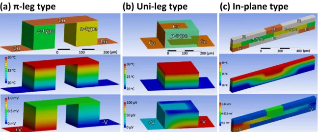
As shown in Fig. 1.10a, a typical thermoelectric generator consists of p-type and n-type legs for hole and electron conduction, respectively. This structure, which is called π-leg type, achieves electrical series connection and thermal parallel connection by placing each element in a π-shape (overall electrical conduction is in the plane of the substrate and thermal conduction is normal to the substrate). However, in addition to the scarcity of good candidates for n-type materials, the balance of p- and n-type legs must also be taken into account. Because of differences in the transport coefficients (i.e., 𝑺, 𝛔 and 𝜿) of p and n materials, unbalanced structures will lead to a loss of power output.
20
Figure 1.10: Schematic of heat conduction and electric field distribution at steady state of (a) π-leg type, (b) uni-leg type and (c) in-plane type thermoelectric generators when the temperature gradient is applied perpendicular to the substrate.
Compared with the conventional π-leg type module, the uni-leg type module reduces some of these problems (Fig. 1.10b). The uni-leg type, in which the top electrode is directly connected to the bottom electrode of the adjacent device, does not need both p and n materials like a π-leg module. Instead, uni-leg type modules enable the generation of power by using only one type of thermoelectric material (p-type or n-type).6 A drawback of the uni- leg design is that the intermediate electrodes can provide a highly conductive thermal path from the hot side to the cold side, resulting in a smaller temperature gradient and output power.
Generally, having the longest thermal and electrical conduction paths (i.e., the thickest active layer) possible while maintaining flexibility is very important for flexible organic thermoelectric modules because a larger temperature gradient from the same heat source can be obtained with a thicker layer. Recently proposed in-plane-type modules can overcome the need for a thick active layer by incorporating a heat spreader as shown in Fig. 1.10c.52 The heat spreader creates a horizontal temperature gradient from a vertical one, making both thick or thin active layer compatible with in-plane modules.
(a) π-leg type (b) Uni-leg type (c) In-plane type
21
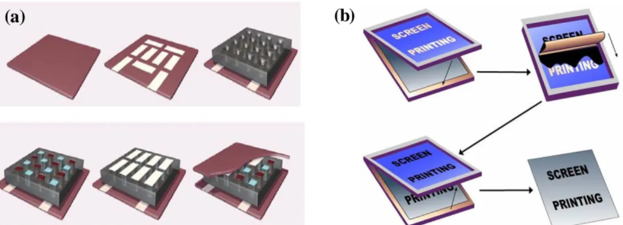
Figure 1.11: Existing processes for making organic thermoelectric modules: (a) micro- cavity-assisted ink-jet process and (b) screen-printing process.
Micro-cavity-assisted ink-jet (Fig. 1.11a), one of the most studied methods for fabricating modules, has limits on the properties of the polymer-containing solutions (e.g., solvent type, temperature, viscosity, and pH) that can be used with inkjet nozzles.9 Furthermore, the rigid epoxy-based micro cavities that are used to prevent the spreading of ink and help form the thick active layers are a cause of heat leakage and lower the mechanical flexibility of the module. Screen printing (Fig. 1.11b), an alternative fabrication method, also has the problems of poor film-forming properties and the need for ink development.6 Thus, stable and reliable patterning technologies must be developed to make high-density thermoelectric modules.
1.3.5 State-of-the-art and challenges for OTEGs
Because the carriers in inorganic thermoelectric materials conduct by band conduction (not hopping conduction), the Seebeck coefficient is proportional to the temperature, but the thermal and electrical conductivity follow an inverse relationship with temperature (Fig.
1.12a). Thus, inorganic thermoelectric materials designed for high temperature operation exhibit low 𝒁𝑻̅ at room temperature because of low Seebeck coefficients and high thermal conductivities. Figure 1.12b summarizes the highest 𝒁𝑻̅ in various inorganic thermoelectric materials as a function of temperature.53–65
(a) (b)
22
Figure 1.12: (a) Thermoelectric properties of spark-plasma-sintered PbTe:SrTe:Na, which exhibits that best 𝒁𝑻̅ value for a p-type material of 2.2 at 915 K.65 (b) The dimensionless thermoelectric figure of merit(𝒁𝑻̅) for the best inorganic thermoelectric materials as a function of temperature. (Data from the Kanatzidis Research Group and the Office of Naval Research).
Compared with inorganic thermoelectric materials, there are still many remaining challenges to the widespread use of organic thermoelectric generators even though many organic materials have already been screened. Figure 1.13 summarizes the thermoelectric properties of many of the best-performing organic material systems. In addition, the properties of BiTe-based inorganic materials are also included because their high 𝒁𝑻̅ values for p-type and n-type operation near room temperature make them the best inorganic thermoelectric material in the operating region where organic materials are expected to be most promising.65
300 400 500 600 700 800 900 1000 200
400 600 800 1000 1200 1400 1600
Electrical conductivity, σ (S cm−1 )
Temperature (K)
σ
50 100 150 200 250 300 350 S
Seebeck coefficient, S (μV K−1 )
0.0 0.5 1.0 1.5 2.0 2.5 3.0
κ
Thermal conductivity, κ (W m−1 K−1 ) (-)
Temperature (K)
(a) (b)
23
Figure 1.13: Thermoelectric properties of representative (a) p-type and (b) n-type organic materials at room temperature. Diagonal lines: Equivalence power factor (𝑺𝟐𝝈) line for each value.
Recent progress using PEDOT, one of the most studied p-type thermoelectric materials, has yielded remarkably high performance comparable to that of inorganic materials. However, a lack of good candidates for n-type materials is a serious problem. Therefore, in addition to p-type materials, further research of n-type thermoelectric materials that have high thermoelectric energy conversion efficiencies and good processibility is essential. Of course,
101 102 103 104
101 102 103
(Clevios PH1000) PEDOT:PSS PEDOT:Fe3+-tos3
P3HT: Fe3+-tos3·6H2O
PEDOT:PSS:DMSO:EG P(KX[Cuett]) (Bulk) CNT:O2
PA:I2 BiTe(Bulk)
S2σ= 100
104
102
Seebeck coefficient, S (μV K−1 )
Electrical conductivity, σ (S cm−1)
101 102 103 104
-101 -102 -103
CNT:dppp CNT:PEI:NaBH4
C60:K CNT@CoCp2 P(KX[Niett]) (Bulk)
P(NaX[Niett]) P(PymPh):NaNap
TTF:TCNQ
BiTe(Bulk)
S2σ= 100
104
102
Seebeck coefficient, S (μV K−1 )
Electrical conductivity, σ (S cm−1)
(a)
(b)
Goal for OTEGs
~1.0
~0.5 W m−1K−1
~1700 μW m−1K−2
~1.0
~1.0 W m−1K−1
~1.0
~1.0 W m−1K−1 Goal for OTEGs
~1.0
~0.5 W m−1K−1
~1700 μW m−1K−2
This work
This work
24
being free of rare metals, environmentally stable, and nontoxic are also requirements.
Another challenge is that the transport coefficients of thermoelectric materials (i.e., 𝑺, 𝝈, and 𝜿) are all a function of free carrier concentration as mentioned in Section 1.3.1. Thus, controlling the carrier density in the active thermoelectric materials is necessary for optimizing 𝒁𝑻̅. Although chemical doping is good way to control an organic material’s redox levels, the choices for proper dopants that can transfer charges to the organic materials are limited, and maintaining the doped state of organic material remains a challenge, as mentioned in Section 1.3.3.
Finally, in addition to materials with good thermoelectric properties, connecting a large number of elements in a module is needed to achieve huge thermoelectric voltages and high power output. Microcavity-assisted ink-jet and screen printing, the currently reported processes to make flexible thermoelectric modules, have many problems as mentioned in Section 1.3.4. Thus, a stable patterning technology is required to make thermoelectric modules with a high density of many series connected devices.