• 検索結果がありません。

ポリ(3-ヘキシルチオフェン)の次元制御とその応用の研究

N/A
N/A
Protected

Academic year: 2021

シェア "ポリ(3-ヘキシルチオフェン)の次元制御とその応用の研究"

Copied!
101
0
0

読み込み中.... (全文を見る)

全文

(1)

九州大学学術情報リポジトリ

Kyushu University Institutional Repository

ポリ(3-ヘキシルチオフェン)の次元制御とその応 用の研究

胡, 建臣

https://doi.org/10.15017/1398361

出版情報:Kyushu University, 2013, 博士(工学), 課程博士 バージョン:

権利関係:Fulltext available.
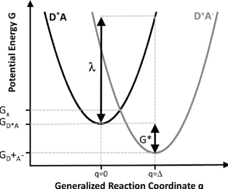
(2)

Study on Dimensional Control of Poly(3- hexylthiophene) and Their Corresponding

Applications

Hu Jianchen

Supervisor: Wakayama Yutaka

Kyushu University

2013

(3)
(4)

Content

Content ………..………...I

Chapter 1. Introduction ………...………1

1.1 Development of polythiophenes (PTs) …………..……….1

1.1.1 Development of unsubstituted PTs………..…1

1.1.2 Development of poly(3-alkylthiophene)s (P3ATs)………..4

1.2 Electric and photoelectric properties of P3ATs and P3HT …...7

1.2.1 Charge carrier mobility and the influence factors………....7

1.2.2 Exciton Formation by absorption of photon………....9

1.2.3 Formation of Charge-transfer excitons………..10

1.2.4 Dissociation of Charge-transfer excitons………...14

1.2.5 Charge Transport………16

1.2.6 Charge carriers recombination………...17

1.3 Current issues of P3HT applications ………...………….….17

1.4 Strategies proposed in this thesis and their motivations ……..20

References ………..23

Chapter 2. Fabrication of sub-1D P3HT nanopillars array and the application in solar cell ………...31

2.1 Introduction ………...31

2.2 Strategy of fabrication of sub-1D P3HT nanopillars and interdigitated solar cell ………...…32

2.3 Information of main chemicals and equipment ………33

2.4 Experimental details ………35

2.4.1 General procedure for the preparation of AAO template……….35

2.4.2 Preparation of P3HT pillars standing on P3HT film………35

2.4.3 Transfer pillars array contained P3HT film to ITO substrate…..35

(5)

2.4.4 Characterization method………...36

2.5 Results and discussion ………37

2.5.1 Dimensional control of P3HT pillars by AAO template………..37

2.5.2 Fabrication of P3HT/C 60 interdigitated p-n heterojunction…….38

2.5.3 Photovoltaic properties of fabricated P3HT/C 60 interdigitated p-n heterojunction and analysis of the preliminary result………40

2.6 Summary ……….…………...…41

2.7 Motivations and significances of this work ………..42

References ………43

Chapter 3. Fabrication of one-dimensional (1D) P3HT nanowires and the improvement of their electrical conductivities ………....47

3.1 Introduction ………..………...48

3.2 Strategy of fabrication of 1D P3HT nanowires doped with F4-TCNQ in different doping level ………...………...48

3.3 Informations of main chemicals and equipments ……..……..50

3.4 Experimental details of fabrication of F4-TCNQ doped P3HT nanowires and films, and the measurement methods ... 50

3.4.1 Fabrication of F4-TCNQ doped P3HT nanowires………...50

3.4.2 Fabrication of F4-TCNQ doped P3HT films………...51

3.4.3 Electrical conductivity measurement of F4-TCNQ doped P3HT nanowires and films………....52

3.4.4 Absorption measurement of F4-TCNQ doped P3HT nanowires and films………..…………54

3.5 Results and discussion ………....54

3.5.1 Resistivity calculation of F4-TCNQ doped P3HT nanowires…..54

3.5.2 Resistivity calculation of F4-TCNQ doped P3HT films………..56

3.5.3 Comparison of the resistivities of F4-TCNQ doped P3HT nanowires and films………57

3.5.4 Analysis of the influence of AAO template on the improvement

of F4-TCNQ doped nanowires conductivities………...58

(6)

3.6 Summary ………...63

3.7 Motivations and significances of this work ………..64

References ………65

Chapter 4. Fabrication of two-dimensional (2D) P3HT:PCBM films and the application in organic solar cell ………..71

4.1 Introduction ………...71

4.2 Strategy of fabrication of 2D ITO/PEDOT:PSS/P3HT:PCBM structure in a large scale …72 4.3 Informations of chemicals and equipments ………...73

4.4 Experimental details ………....75

4.4.1 Fabrication of ITO/PEDOT:PSS/PCBM:P3HT structure……..75

4.4.2 Fabrication of P3HT film on water surface and fabrication of P3HT:PCBM films on water surface………...….76

4.4.3 Fabrication of P3HT film and P3HT:PCBM films transferred to quartz substrates………..76

4.4.4 Fabrication of OPV device and performance measurement…...76

4.5 Results and discussion ………..77

4.5.1 Understanding of the floating phenomenon………...77

4.5.2 P3HT film formed on water surface (Experiment S1)……...77

4.5.3 Effect of PCBM on morphologies of P3HT:PCBM films on water surface (Experiment S2)………80

4.5.4 Effect of PEDOT:PSS on formation of continuous P3HT:PCBM/PEDOT:PSS composite film (Scheme 1)……82

4.5.5 Device performance………...85

4.6 Summary ………...86

4.7 Motivations and significances of this work ………..…..86

References ………..88

Chapter 5. Conclusions and perspective ………..………91

Acknowledgment ………..………...93

(7)
(8)

Chapter 1. Introduction

1.1 Development of polythiophenes (PTs).

1.1.1 Development of unsubstituted PTs

In 1977, Shirakawa and his co-researchers found that iodine (I 2 ) doped polyacetylene (PA) had conductivity [1], which overturned the conception that polymer could not be utilized as conductive material. Besides, this new discovery extended the application fields of polymer materials and promoted their development. During the passed decades, because of the advantages in easily synthesis, separation and recycling [2, 3], a series of conductive polymers were sequential explored, such as polypyrrole (PPy) [4, 5], polythiophene (PT) [6, 7], polyaniline (PAn) [8, 9], poly(3,4-ethylenedioxythiophene) (PEDOT) [10, 11], and poly(phenylene vinylene) (PPV) [12], etc. Untill now, conductive polymer materials are still attractive, even in many fields they are utilized to replace inorganic materials.

Figure 1-1. Synthesis of polythiophene by using precursor 2,5-Dibromothiophene and metallic catalyst nickel(bipyrine)dichloride (Ni(bipy)Cl 2 ). [13]

In the big family of conductive polymers, semiconductive polymers are currently studied to identify, understand and apply the useful optoelectronic properties inherent in the electron-rich π-systems. Many research groups were inspired to study its properties and to find new, effective semiconductive architectures. Conjugated polymers proved the most durable and robust structures with diverse electronic and physical properties easy to design.

Semiconductive polythiophenes (PTs) are such kind of conjugated polymers, possessing the

structure like aromatic rings. In 1980, Yamamoto’s group [13] firstly synthesized PT by

using precursor 2,5-Dibromothiophene and metallic catalyst nickel(bipyrine)dichloride

(9)

(Ni(bipy)Cl 2 ) (Figure 1-1). Then Wochnowski and co-wprkers [14] improved the synthesis method by introducing Uv-vis light as an irradiation source and explained the polymerization mechanism (Figure 1-2).

Figure 1-2. Improved process of synthesis of conductive polythiophene by introducing Uv- vis light as an irradiation source. [14]

In PTs, the thiophene rings couple in the 2 and 5 positions, which allows for the conjugation of π orbitals along the polymer chain, leading to the development of semiconductor/insulator band structure for the solid-state materials. That’s because the electrophilic reactions favor sites α to the sulfur atom, enchaining predominantly 2,5- couplings to form an extended π-system with quasi one-dimensional delocalization[13].

Higher electrical conductivity in PT can be achieved when the material is oxidized (or

doped). The consequence of the oxidation of PT is a prominent change in the electronic

(10)

band structure, namely, new midgap states are created and quinoidal type of resonance structure is formed (Figure 1-3). This allows for the production of charge carriers called bipolarons [15]. The oxidation leads to an effective reduction in the band gap and an increase in the electrical conductivity of the material.

Figure 1-3. Neutral and oxidized forms of polythiophene (R = H or alkyl). [15]

A quinoidal type of resonance structure necessitates that a coplanar orientation of rings be readily accessible, thus a small band gap and high conductivity could be achieved [16].

If high energy constraints prevent the forming coplanar, then a low conductivity will be

resulted. In the solide state, electrical conductivity is attributed two aspects: one is dense

packing of polymer chains which can allow for overlap to occur in three dimensions (3D)

and this 3D conductivity creates low resistivity pathways for carriers (electrons or holes) to

travel; the other one is dense chain packing with overlap of the π orbitals which can also

lead to high electrical conductivities. In general, the processing of the polymer plays a very

important role in controlling the assembly of the 3D structure, determines the polymer

morphology, and influences the resulting electrical conductivity [17].

(11)

On the other hand, a strong tendency to associate causes some intermolecular overlap but also renders PT insoluble and infusible and therefore difficult to characterize. Yamamoto and co-workers traced this effect to regioisomeric couplings. They developed an exclusively 2,5-coupled PT and found the solubility was negligible. Enchaining 2, 4 defects enabled dissolution but caused backbone twisting, electron localization and widened the optical bandgap [18, 19]. In one word, eliminating couplings β to sulfur resulted in the maximization of effective conjugation length, but formed a material with low processability.

1.1.2 Development of poly(3-alkylthiophene)s (P3ATs)

The insolubility and intractability of PTs, difficult to characterize and study, confined their applications [20]. To extend the practical application of PTs, in the molecular design the molecular propertities should be considered, including the solubility, molecular weight, mechanical strength, stability and, of course, the production cost. Solubility improvement was well realized by adding ring substituents, particularly at 3 position. Because the introduction of ring substituents at 3 position caused the reduction of the interaction between the molecular chains, enabling the increasing of solubility. When the number of carbon atoms of the introduced alkyl or alkoxy substituents is no smaller than 4, the substituted PTs could be dissolved in the solvents like chloroform, tetrahydrofuran (THF), chlorobenzene and N-methyl-2-pyrrolidone (NMP) [21]. The incorporation of 3-alkyl substituents results in a loss of symmetry along the polymer backbone, causing the improvement of processability.

Sugimoto and co-workers reported that FeCl 3 -mediated polymerization afforded high molecular weight poly(3-alkylthiophene)s (P3ATs) (Mn = 30,000-300,000) [22].

Nevertheless, switching from symmetric thiophene to asymmetric 3-alkylthiophene

reintroduces a problem of structural inhomogeneity, which is attributable to regiochemical

isomers. This result was obvious observed in the NMR spectrum [23, 24]. The complexity

arises from poorly controlled coupling of the asymmetric monomer (Figure 1-4). The

chemical environment for a given ring in a homopolymer depends on the orientation of

both neighbors, requiring four regioisomeric triads for complete description: head-to-tail

(12)

with head-to-tail (HT-HT), tail-to-tail with head-to-head (TT-HH), head-to-tail with head- to-head (HT-HH) and tail-to-tail with head-to-tail (TT-HT). The irregulation of the side chain orientations causes polymer twisting because of the their hindrance. Normally, the twisting confines polymer conjugation and widens the band gap, impacting polymer properties, like conductivity. In contrast, regular (HT-HT) poly(3-alkylthiophene)s are easily to form planar structure with lower band gap and higher conjugation. In addition, these regular P3ATs exihibit fast and large nonlinear optical responses [25, 26], photo- and electroluminescence [27, 28] behavior, and other band gap dependent phoenomena.

Figure 1-4. Traditional syntheses incorporate multiple regioisomers. [23, 24]

(13)

Figure 1-5. Synthesis of regioregular poly(3-alkylthiophene) by McCullough method. [29]

To achieve a high regulation, in 1992, McCullough R K and co-workers [29] firstly reported their synthesis of regioregular P3AT, and the HT regulation was higher than 98%

(Figure 1-5). In 1995, they improved the synthesis technology [30] to reduce by-product types and increase productivity of regioregular P3AT with HT structure (Figure 1-6). In 2008, Seung and co-workers improved synthesis process by using active zinc powder under room temperature, reducing the product cost [31].

Figure 1-6. Synthesis of regioregular poly(3-alkylthiophene) by improved McCullough method. [30]

In brief, by meaning of introducing ring substituents at 3 position and forming HT

regular P3ATs, the solubility is well improved. One the other hand, P3ATs remain the

conductivity of unsubstituted PTs [32].

(14)

1.2 Electric and photoelectric properties of P3ATs and P3HT

1.2.1 Charge carrier mobility and the influence factors

For organic semiconductors to be valuable in most practical applications, a charge carrier mobility of at least 0.1 cm 2 V −1 s −1 is needed (with on/off ratio greater than 10 6 ) [33]. Bao first report of a relatively high charge carrier mobility for a conjugated polymer was obtained using regioregular poly(3-hexylthiophene) (rr-P3HT), at the level of 0.045 cm 2 V −1 s −1 [34]. Later, Sirringhaus improved mobilities in the range 0.05-0.1 cm 2 V −1 s −1 for rr- P3HT [35]. Regioregularity is critical for good electrical properties [36].

rr-P3HT has been extensively used for studying factors that impact charge carrier mobility, such as processing conditions [37], surface treatment [35] and molecular weight [38]. Generally, the best mobilities are obtained using relatively high molecular weight rr- PHT (Mn >25 k) under slow evaporating conditions on hydrophobic substrates. These conditions promote self-organization of rr-P3HT with the π–π stacking direction perpendicular to the substrate surface, and also good interconnectivity of crystalline domains [39].

Molecular weight and processing influence the field effect mobility. Zhang et al. showed that careful processing of rr-P3HT samples with narrow molecular weight distributions allows assembly into nanofibrils with contour length corresponding to the polymer length [40]. Field effect mobility increased exponentially with nanofibril width. The width of nanofibrils initially increased linearly with Mw and then leveled off. Yang et al. [41]

observed nanofibrils for slower cast films of rr-P3HT and the nanofibril width also did not increase with molecular weight above a certain molecular weight threshold. They argued that chain folding limits the nanofibril width and that the resulting entanglements lower crystallinity and mobility [42]. It can be concluded that higher mobility could be obtained if the chain folding could be prevented.

Another important factor that influences mobility in conjugated polymers is charge

carrier density: mobility tends to increase with charge carrier density as traps become filled

(15)

[43]. Furthermore, when the charge density is sufficiently high, conjugated polymers can reach a very high conductivities like metal-insulator boundary [44].

The studies on effect of side-chain length on field effect mobility suggest that a longer side-chain length is detrimental to field effect mobility. It is suggested that the alkyl side- chains act as a barrier to charge transport between π-conjugated main chains. In 2005, Babel and Jenekhe demonstrated that P3HT was in fact the best, followed by P3BT, P3OT and P3DDT [45].

Both water and oxygen are responsible for the lower on/off ratio, moisture being the dominant factor [46]. High on/off ratios and good stability can be obtained if rr-P3HT is kept under an inert atmosphere [35, 47].

Another related issue with rr-P3HT is its environmental stability. Because of its relatively low ionization potential, rr-P3HT may be susceptible to oxidation in wet air [48].

Furthermore, PTs can undergo photochemical reactions and therefore must be protected from the combination of light and oxygen [49].

In the absence of light, oxygen was not a strong dopant for any of these polymers.

Instead, ozone was found to be a strong dopant for PT polymers. Above results explain the variations in stability reported in the literature and suggest that environmental stability studies should be conducted in controlled environments in order to define realistic limits to stability.

The conduction mechanism in polythiophene is the subject of intense investigation [50].

One of the most basic questions still to be answered to understand conductivity and

electronic properties in doped PTs remains whether the charge carriers in doped PTs are

spinless bipolarons or spin-carrying polaron pairs. Correctly answering this question is

crucial for the design and application of PT-based organic semiconductor devices. Initial

experimental studies [51] of highly doped PT showed the bipolaron structure to be

dominant. Later, this finding was supported by theoretical studies [52].

(16)

1.2.2 Exciton Formation by absorption of photon

Inorganic semiconductors have rather high dielectric constant ( ε > 10), thus enabling promotion an electron from the valence band to the conduction band by absorbing a photon, resulting in a free electron in the conduction band and a free hole in the valence band.

Screened by the surrounding material, these two charge carriers usually do not feel their mutual electrostatic attraction except at very low temperatures under which the kinetic energy of the charge carriers lower than their Coulomb attraction and they form a bound state termed an exciton.

For organic semiconductors, the the dielectric constant is much lower (ε ≌ 3-4), causing the electrostatic attraction between the charge carriers not screened as efficiently. This leads to a much stronger attraction between the charge carriers and ultimately to binding energies of more than 0.5 eV that far exceed the thermal energy at room temperature [53].

At the end of last century, It was argued that whether free charge carriers or bound excitons comprise the primary photoexcitations in conjugated polymers. An agreement was made on that excitons indeed are the primary photoexcitation, mainly because photoexcitation near the bandgap does not directly lead to photoconduction as would have been expected for the generation of free charge carriers [54]. One consequence of this is that optical excitation does not lead to a transition of an electron from the highest occupied molecular orbital (HOMO) to the lowest unoccupied molecular orbital (LUMO), but to a transition to an exciton state that is lower in energy than the LUMO by the binding energy of the exciton.

Three models were found for excitons: Wannier-Mott model was found in inorganic

semiconductors and excitons are delocalized over several lattice constants, Frenkel model

was found on the basis of excitons are localized on single sites such as small molecules or

single conjugated segments of a polymer chain. Charge transfer excitons, comparing to

Frenkel excitons, apart from that the two charge carriers are not located on the same site,

insteading, on two adjacent sites. These sites can be within the same polymer chain, on two

(17)

identical neighboring molecules or even on different adjoining molecules. Depending on the charge carriers spinning orientation, excitons are defined as singlets and triplets, for the former the spins are anti-parallel (total spin 0) and for the latter the spins are parallel (total spin 1). Carbon bonds determine that the ground state of organic molecules is always a singlet state. It is essential to have a change in the symmetry of the wave function for a dipole transition between a ground and an excited state and this change can only be achieved by a change in the angular momentum quantum number (∆l = ±1). A photon involved in such a transition can compensate this change with its spin (s = 1), but an additional change in the spin for counteracting is unexpected. This explains why it is spin- forbidden for optical transitions between the singlet ground state and the triplet excited state , also explains optical excitation of organic molecules leads to the formation of singlet excitons. Nevertheless, sometime transitions between singlet and triplet states are available, a precondition of which is that the difference in spin is compensated by the molecule, such as spin-orbit coupling in the presence of heavier atoms like sulfur or by spin-lattice relaxation. This process is termed intersystem crossing and typically occurs on a time scale of 10 -10 to 10 -8 s [55].

1.2.3 Formation of Charge-transfer excitons

Preceding section established that in organic semiconductors the formation of a strongly bound singlet exciton by absorption of a photon. Dissociation is essential for obtaining free charge carriers, which can be achieved by blending two organic semiconductors in different energy levels, thus it is favorable for an electron to undergo a charge-transfer process from the bound singlet exciton state to a less tightly bound charge-transfer exciton.

Marcus [56] theoretically intuitively described charge-transfer reactions, and then Jortner

[57] extended it to a full many-particle quantum mechanical analysis. The detailed

introduction to charge-transfer theory can be found in reference [58].

(18)

Figure 1-7. Quantum well and potential energy surfaces relevant for charge transfer.

Arrows indicate fluctuations about the generalized reaction coordinate leading to changes in the energy levels of the quantum wells which corresponds to oscillations along the potential energy surface [58].

A simplified quasi one particle model was established to describe the movement of an

electron in the potential energy landscape created by the atomic nuclei of the donor and the

acceptor sites involved in the transfer of an electron from an excited donor site D* to an

acceptor site A in the form D*A→D + A - . This potential energy landscape essentially creates

donor and acceptor quantum wells with width and depth depending on the momentary

configuration of the atomic nuclei. Such quantum wells along with the corresponding

electronic energy levels are illustrated on the left side of Figure 1-7. Assuming no energy

exchange between the electron and its environment, the electronic energy levels of the

donor and the acceptor have to be equal in order to satisfy the conservation of energy

during the transfer. Consequently, all nuclei involved in the transfer process have to

reorganize by statistical fluctuations about their equilibrium positions, by meaning of which

the energy levels in the donor and the acceptor quantum well match. This can also be

illustrated with the help of so called potential energy surfaces. On the right side of Figure 1-

7 these potential energy surfaces before (labeled D*A) and after charge transfer (labeled

(19)

D + A - ) are represented by parabolas plotted against a generalized reaction coordinate accounting for all degrees of freedom of the nuclear configurations. As indicated by arrows in Figure 1-7, vibrations, rotations and similar fluctuations of the nuclei cause the system to oscillate along the potential energy surface D*A. When the system reaches the point where the energy of the states before and after charge separation are identical (link of the parabolas), charge transfer can occur.

In classical Marcus theory the molecular fluctuations along a potential energy surface are described by harmonic oscillations about an equilibrium position (minimum of a parabola).

Figure 1-8 shows the definition of the parameters used for describing the problem. Both potential surfaces are assumed to be parabolas with identical curvature c. The equilibrium configurations of the initial (D*A(q) = cq 2 + G D*A ) and of the charge transferred ( D + A - (q)

= c(q-∆) 2 + G D + A - ) states are denoted with q = 0 and q = ∆ and they are energetically displaced by the value of G* = G D*A – G D +

A - . G B * is the energy barrier the system needs to overcome before charge transfer can occur and G X is the intersection of the parabolas. The reorganization energy λ = D*A(∆) - D*A(0) = c∆ 2 is defined as the amount of energy that would be needed to change the molecular configuration of the initial state to that of the equilibrium position ∆ of the charge transferred state. It can be divided into a so called inner sphere describing the contribution of the molecule(s) directly involved in the transfer process and outer sphere contribution referring to all molecules in the closer vicinity of the directly involved molecule(s). In other words, through the formalism of reorganization Marcus’ theory explicitly takes the polaronic nature of charge carriers into account by considering the energy it takes for a charge carrier to move its associated lattice distortion along during the transfer process. All energies mentioned here are Gibbs free energies to account for entropic effects.

From geometrical considerations, the energy barrier is given by G B( 4 G *)

2

. While the

reorganization of the system directly forms a barrier for charge transfer, the influence of the

energetic displacement G* of the equilibrium configurations is a bit more complicated. In

the regime 0>G*≥-λ it acts as a driving force for charge transfer by decreasing the energy

(20)

barrier. However, if the absolute value of G* exceeds λ, G* < -λ, it has the opposite effect and increases the barrier. In thermodynamic equilibrium the charge-transfer rate of the system can be determined by Boltzmann statistics as

( * ) 2

exp[ ] exp[ ]

4

B CT

B B

G G

k A A

k T k T

     (1-1)

with Boltzmann’s constant k, at Temperature T, and with the coupling constant A that depends on the specific type of transfer reaction (e.g. intra- or intermolecular transfer).

Figure 1-8. Potential energy surfaces of the initial (D*A) and the charge transferred (D + A - )

state approximated by parabolas. [58]

(21)

In some cases not every site in a material is suitable for charge transfer so that an additional transport step precedes the transfer process. Comparing to the actual transfer time, if this transport step is slow the overall rate of the transfer process is reduced. For a transport mechanism of three dimensional isotropic diffusion an estimation of the reduced transfer rate can be obtained. Assuming an excitation has to travel a distance x on average between the site where it was created and a site suitable for charge transfer, the average rate k D for the excitation to reach a transfer site is given by

D 2

k D

x (1-2) with diffusion constant D. The total charge-transfer rate k CT in the limit of very fast transfer and very slow diffusion can be approximated by the diffusion rate k CTk D . If the phases segregate of blending organic semiconductors form large, pure domains so that the diffusion time of excitons to the interface between the phases is larger than the duration of the charge-transfer process itself, diffusion limited charge transfer can be found. For a diffusion constant of D = 10 -3 cm²/s and assuming that the charge-transfer time is lower than 100 fs, an average diffusion distance of as little as 0.1 nm will lead to a diffusion limited charge-transfer rate [59]. In blends for efficient organic solar cells domain sizes usually exceed 1 nm, so it seems likely that diffusion indeed limits the charge-transfer rates in such systems. Cowan et al. recently argued that for organic solar cells, excitons in donor- polymers are initially highly delocalized and relax into more localized excitons on a timescale comparable to charge transfer. Such an initial delocalization has effect on increasing the critical domain size at which diffusion effects start to become important.

1.2.4 Charge Separation: Dissociation of Charge-transfer excitons

The morphology have a huge influence on the separation of charge-transfer excitons in

various ways and consequently on a broad range of length scales. These scales range from

the orientation of molecules at the interface to the formation of interpenetrating phase

(22)

segregated networks of blended materials. A variety of methods for controlling the morphology have been developed experimentally. Among these are variations of the sample preparation conditions, like using different solvents [60] or annealing conditions [61], introducing smaller modifications in the molecular structure like a replacement of side-chains [62]. All of these approaches have in common that they involve rather subtle changes within a series of samples under study in order to keep secondary effects that could influence charge separation

Two processes determine the optimal size for nanoscale phase segregation in terms of charge separation. One is an upper limit given by the exciton diffusion length. If the phase domains are larger than this diffusion length, not all excitons will reach the interface to undergo charge transfer but will recombine insteadly. On the other hand the charge carriers have to be able to move far enough from the interface to be considered spatially separated.

Veldman and Quist found that the larger phase segregation is beneficial for the dissociation of charge-transfer excitons. Annealing in P3HT:PCBM was found to have a similar effect [61] and the simultaneous recovery of the photoluminescence [62], indicating an incomplete exciton quenching. These results further supported the conclusion that larger pure phase domains lead to a more facile dissociation of charge-transfer excitons.

Holcombe et al. [63] found that a larger distance between the donor and acceptor molecules resulted in a reduced charge-transfer exciton binding energy and a higher dissociation probability, showing that the precise interfacial structure strongly impacts the formation of spatially separated charges.

Liu et al. performed molecular dynamics simulations explicitly accounting for structural

variability at the interface of P3HT:PCBM [64]. They concluded that either charge

separated states or charge bridging states that can be assigned to charge-transfer excitons

can be formed after the dissociation of a singlet exciton at the interface depending on the

exact interface geometry.

(23)

Further theoretical calculations and experiments suggest that certain molecular arrangements can cause the formation of dipoles at the interface which can reduce the Coulombic attraction between an electron and a hole in a charge-transfer exciton, thus the dissociation probability increase [65].

1.2.5 Charge Transport

Charge transport repeats itself in the physical mechanisms as an omnipresent motif, which govern the device performance of organic solar cells. That is the reason why a detailed understanding of the underlying principles of charge transport is very important when trying to correlate molecular structures, charge transport properties and device performance.

Unlike inorganic semiconductors, organic semiconductors have no translational symmetry, but instead they have an ensemble of localized sites with slightly varying energetic levels and distances between them. Bässler [60] observed the sites that are very low in energy can act as traps for charge carriers, because they accept charge carriers very quickly but release them only slowly. Spatially isolated sites however cannot trap charges as efficiently because of the symmetry of the trapping and detrapping rates [61].

It was also found that [62] at high temperatures the charge carriers created in a sample can equilibrate within the density of states much faster than their average transit time through the sample. Consequently, the average charge carrier mobility obtained from an experiment is dependent of the equilibrium charge carrier mobility and is independent of the sample thickness.

At the temperature below critical temperature (Tc) the time needed for equilibration is longer than the transit time of charge carriers through the sample. This means that the charge carrier mobility determined from an experiment would no longer be the equilibrium charge carrier mobility, and the actual value would strongly depend on the sample thickness.

These two regimes of charge transport are termed non-dispersive and dispersive charge

transport, respectively.

(24)

1.2.6 Charge carriers recombination

The most basic requirement for recombination of independently moving opposite charge carriers (i.e. electrons and holes) is that they approach each other close enough to enter their mutual capture radius. This random process is basically dominated by the probability of two charge carriers meeting. This kind of recombination was first described by Langevin [53] for the recombination of ions in gases.

An important requirement for Langevin recombination to be applicable is that the mean free path of a charge carrier (i.e. the typical length scale of the motion of a charge carrier) is much shorter than the capture radius of two opposite charges. The typical length scale of charge motion in organic semiconductors can be considered to be limited either by the dimension of the conjugated system of the site or by the hopping distance between neighboring sites. In any case it is well below the Coulomb capture radius of more than 10 nm, so that this prerequisite can be considered fulfilled in disordered organic semiconductors.

Essentially, the recombination rate increases if there are more charge carriers and if the charge carriers move faster. In blends of organic semiconductors, as used for solar cell devices, electrons and holes are each confined to one of the material phases, thus recombination can only occur at an interface. This effectively decreases the recombination rate.

As has been pointed out by Juska et al. [63], the reaction order of the recombination can also be limited by the dimensionality of the charge carrier motion.

In brief, recombination strongly depend on the exact morphology of a sample that can be influenced not only by material properties but also by sample preparation conditions.

1.3 Current issues of P3HT applications

After the development of more than 20 years, synthesis of P3ATs is already

industrialized. The applications are also extened to many fields. Among them, poly-3-

hexylthiophene (P3HT) is one of the most extensively studied conjugated polymer because

(25)

of its relatively high carrier mobility coupled with solution processability [34, 35].

P3HT applications run from light-emitting diodes [70] to thin-film transistors [71].

Moreover, P3HT coupled with inorganic materials (e.g. TiO 2 [72], ZnO [73], carbon nanotubes [74], phenyl-C61-butyric acid methyl ester [75]) is an excellent component for use in low-cost photovoltaics. Polythiophene-based solar cells have reached power conversion efficiencies of about 7.4% [76].

The applications of P3HT are mainly based on its electrical and photoelectric properties, especially in the application of solar cell and improvement of its conductivity. Nevertheless, there are still some issues to be settled:

(1) For fabrication of P3HT-base organic solar cell, the spin coating method has been established as the most reliable and reproducible process using the solution process.

However, material waste is unavoidable in spin coating process. Moreover, this method is only suitable for a limited substrate size. For the future application of polymer solar cells (PSCs), somethings should be considered about, such like the production cost should be minimized, the producing process should be continuous and a high throughput should be achieved. Besides, the technique should be able transfer to the flexible substrates with large area, which is the main advantage of PSCs. During the passed decades, new deposition techniques have been demonstrated for PSC fabrication including ink-jet printing, spray coating, and screen printing. Each method was proposed to avoid the disadvantages of spin coating technique, but unfortunately, all these techniques require costly equipment. In contrast, the dip coating technique has been developed as a cost effective method but it cannot be applied to soft substrates because organic solvent may dissolve the plastic substrate during solution processes. Therefore, new technique should be found to fabricate large-scale PSCs at low cost with inexpensive equipment and little material waste.

Moreover, the improved technique should be easily applicable to soft substrates such as polyethylene terephthalate.

(2) Development of effective fabrication techniques to produce polymer solar cell is one

aspect for the further application. On the other hand, cell performance is the most important

(26)

parameter to evaluate the application prospect. The high performance should be harvested from the cells designed and prepared on the basis of well understanding of the material properties. Bulk heterojunction (BHJ) solar cells, the most reliable representative, are superior to single- and double-layer cells. The BHJ structure can be formed simply by mixing a donor and acceptor solution. This straightforward technique is advantageous in terms of increasing the donor/acceptor (D/A) interface, which provides the exciton dissociation sites. Meanwhile, a weak point as regards BHJs is that the pathways of the generated carriers are not ensured because of the random phase separation of the respective materials, namely, isolated domains may exist in each other. To ensure exciton dissociation and carrier collection, continuous percolation pathways are required.

An ideal structure would be an interdigitated interface, where the donor and acceptor phases are separate. The diameter and interspatial distance of the pillars should preferably be comparable to the diffusion length of the excitons, which is of the order of 10 nm. Then, the excitons can diffuse to the D/A interface during their lifetime. Furthermore, the interdigitated structure must be aligned perpendicularly to connect with the electrodes so as to provide direct pathways for efficient charge transportation. Meanwhile, the film thicknesses should be around 100 to 200 nm to absorb the incident light and to confine the series resistance. For these reasons, the dimensions of the interdigitated structures should be carefully designed to enhance photovoltaic effects. Interdigitated structures have been obtained using different techniques including self-organization and nanoimprinting.

However, there is still room for further optimization of the dimensions.

(3) Poly(3-hexylthiophene) (P3HT) has high field-effect mobility of 0.2 cm 2 V -1 s -1 , which is the highest reported for a polymer. Such a high mobility is caused by the formation of a lamellar structure by the self assembly of alkyl side chains. Except head-tail (H-T) regioregularity, the conductivity of P3HT depends on processing condition; e.g., the spin-coated samples have 2 orders higher conductivity than that of the solvent-cast film.

However, for organic semiconducting devices molecular doping is preferable, since field-

induced drift of the relative large-size charged molecular dopants can be suppressed. By

(27)

using iodine (I 2 ) as dopant the conduction in P3HT films could be enhanced, but different doping level should be performed by different techniques. Furthermore, in regionrandom P3HT (RRa-P3HT) the doping level achieved was found be higher than that in regioregular P3HT (RR-P3HT), indicating that I 2 was absorbed more deeply into RRa-P3HT than RR- P3HT. But RR-P3HT is much more popular in most applications because its better electrical properties. Recently, P3HT based OFETs doped with the strong acceptor 2,3,5,6- tetrafluoro-7,7,8,8-tetracyanoquinodimethane (F4-TCNQ) have been reported, in which P3HT works as a hole transport material. Meanwhile, F4-TCNQ can function as acceptors that increase the hole density owing to the high electron affinity of cyano groups and fluorine atoms. A advantage for F4-TCNQ is that it can be dissolved together with P3HT.

In these applications, a challenging task is to achieve uniform doping and thus improve the conductivity of P3HT. Besides, because of the dismatch of P3HT and dopant, the doping level is always limited.

1.4 Strategies proposed in this thesis and their motivations

Material properties decide the possibilities of the material applications. In the

applications, the preference of the material properties should be maximized. As an example,

the electrical and photoelectric properties of organic semiconductors make it possible to

apply these materials in many fields like discussed in Section 1.2 and 1.3. P3HT, a typical

representative, was widely studied in many fields, especially in organic field effect

transistor and organic solar cell. In organic devices, morphology strongly influences device

properties, since the morphology can impact on the material electrical or photoelectric

properties, such as carrier mobility, exicton generation and dissociation, carrier

transportation and recombination. Therefore, in the relevant applications, reasonable

designs on device structure, particularly nanostructure, are essential for improving device

performances. On the basis of these reasons, in this thesis, we focus on the dimensional

control, sub-1D, 1D and 2D, of P3HT in nanoscale and verify their applications in the

relevant fields.

(28)

(1) Fabrication of sub-1D P3HT nanopillars and the application in organic solar cell We employed an anodic aluminum oxide (AAO) template to prepare a poly(3- hexylthiophene) (P3HT)/fullerene (C 60 ) interdigitated structure to enlarge the D/A interface.

P3HT absorbs the light from 400 to 700 nm to generate excitons. Meanwhile, C 60 absorbs the light in the UV range of 300 to 400 nm and acts as an electron acceptor to transport such electrons to the electrode. This strategy has the following merits: Firstly, the sub-1D pillar size can be well controlled as regards diameter, interval, and height, making it close to the exciton diffusion length. Secondly, because the pillars and the P3HT film are integrated, a carrier pathway can be formed, which is directly connected to the electrodes.

Finally, self-standing pillars can be fabricated uniformly over a large area. Besides, because of the phase separation, no isolated domains exist. With this technology, costly imprinting equipment and cumbersome processes like dry etching are avoidable.

(2) Fabrication of 1D P3HT nanowires doped with dopant and the improvement in conductivity

We employed AAO as templates to fabricate 1D P3HT nanowires doped with F4-TCNQ.

A great advantage of the AAO template is that a large number of nanowires with a uniform diameter and length can be readily produced. In this strategy, the capillary force in the nanopores of the AAO template compels the chemical dopants to mix into the main matrix at a high doping level, resulting in enhanced conductivity in the molecular nanowires. Such high conductivity is not achievable with the conventional two-dimensional (2D) thin film geometry due to dopant segregation.

Methodologically, to measure the resistivity in individual nanowires precisely, we

employed a four-probe scanning tunneling microscope (STM), which was integrated with a

scanning electron microscope (SEM). The four-probe STM technique has significant

benefits in providing stable contacts, suppressing the contact resistance effect, accessing

individual measurement nano-objects, and especially in allowing multiple measurements on

the same nanowires. Results show that the resistivities of P3HT/F4-TCNQ nanowires were

(29)

tuned in the range of 0.1-10 Ωcm by changing the F4-TCNQ concentration from 10 to 0.1 wt., which were 2-4 orders of magnitude smaller than those of the corresponding P3HT/F4- TNCQ thin film composites. In contrast, the resistivities of F4-TCNQ doped P3HT films were around 4-5 × 10 3 Ωcm, almost independent of the F4-TCNQ concentration.

(3) Fabrication of 2D ITO/PEDOT:PSS/P3HT:PCBM mutilayered structure with a one- step technique and its application in solar cell

We described a one-step fabrication technique for large-scale indium tin oxide/poly(3,4- ethylenedioxythiophene):poly(styrenesulfonate)/ poly(3-hexylthiophene-2,5-diyl):[6,6]- phenyl-C61-butyric acid methyl ester (ITO/ PEDOT:PSS/P3HT:PCBM) multi-layered structures that uses a solution process. The structure was formed by droping P3HT:PCBM solution on the surface of PEDOT:PSS solution in which ITO/glass substrate was immersed.

After solvent evaporation, the substrate was picked up and thus the formed P3HT:PCBM

films could be transferred to the PEDOT:PSS covered substrate. We show that this process

is achievable under very simple conditions. Several motivations could be attained by this

method: simple method, inexpensive equipment, no material waste, thickness controllable

and large area. Preliminary device properties show that the fabricated structure can be used

for organic solar cells.

(30)

References

[1] Shirakawa, H; Louis, E. J.; MacDiarmid , A. G.; Chiang C. K.; Heeger, A. J. Synthesis of Electrically Conducting Organic Polymers: Halogen Derivatives of Polyacetylene, (CH) x . J. Chem. Soc., Chem. Commun. 1977, 16, 578-580.

[2] Hiraishi, K.; Masuhara, A.; Nakanishi, H.; Oikawa, H.; Shinohara, Y. Evaluation of Thermoelectric Properties of Polythiophene Films Synthesized by Electrolytic Polymerization. Jpn. J. Appl. Phys. 2009, 48, 0715011-0715014.

[3] Shinohara, Y.; Ohara, K.; Nakanishi, H.; Imai, Y.; Isoda, Y. Thermoelectric Properties of Poly(3- alkylthiophenes). Mater. Sci. Forum 2005, 492- 493, 141-144.

[4] Diaz, A. F.; Castillo, J. I.; Logan, J. A.; Lee, W. Y. Electrochemistry of Conducting Polypyrrole Films. J. Electroanal. Chem. 1981, 129, 115-132.

[5] Li, X. G.; Li, A.; Huang, M. R.; Liao, Y.; Lu, Y. G. Efficient and Scalable Synthesis of Pure Polypyrrole Nanoparticles Applicable for Advanced Nanocomposites and Carbon Nanoparticles. J. Phys. Chem. C 2010, 114, 19244-19255.

[6] Li, X. G.; Li, J.; Huang, M. R. Facile Optimal Synthesis of Inherently Electroconductive Polythiophene Nanoparticles. Chem.-Eur. J. 2009, 15, 6446- 6455.

[7] Waltman, R.; Bargon, J.; Diaz, A. Electrochemical Studies of Some Conducting Polythiophene Films. J. Phys. Chem. 1983, 87, 1459-1463.

[8] Macdiarmid, A. G.; Chiang, J. C.; Richter, A. F. Polyaniline: A new Concept in Conducting Polymers. Synth. Met. 1987, 18, 285-290.

[9] Li, X. G.; Huang, M. R.; Duan, W.; Yang, Y. L. Novel Multifunctional Polymers from

Aromatic Diamines by Oxidative Polymerizations. Chem. Rev. 2002, 102, 2925-3030.

(31)

[10] Greczynski, G.; Kugler, T.; Salaneck, W. Characterization of the PEDOT-PSS System by Means of X-ray and Ultraviolet Photoelectron Spectroscopy. Thin Solid Films 1999, 354, 129-135.

[11] Choi, J.; Cho, K.; Yim, J. Micro-patterning of Vapor-phase Polymerized Poly (3, 4- ethylenedioxy thiophene) ( PEDOT) Using Ink-jet Printing/Soft Lithography. Eur. Polym. J.

2010, 46, 389-396.

[12] Cernini, R.; Li, X. C.; Spencer, G. W. C.; Holmes, A. B.; Moratti, S. C.; Friend, R. H.

Electrochemical and Optical Studies of PPV Derivatives and Poly(aromaticox adiazoles).

Synth. Met. 1997, 84, 359-360.

[13] Yamamoto, T.; Sanechika, K.; Yamamoto, A. Preparation of Thermostable and Electric-conducting Poly(2,5-thienylene). J. Poly. Sci. Polym. Lett. Ed. 1980, 18, 9-12.

[14] Wochnowski, C.; Metev, S. UV-laser-assisted Synthesis of Iodine-doped Electrical Conductive Polythiophene. Appl. Surf. Sci. 2002, 186, 34-39.

[15] Bredas, J. L.; Street, G. B. Polarons, Bipolarons, and Solitons in Conducting Polymers.

Acc. Chem. Res. 1985, 18, 309-315.

[16] Baughman, R. H.; Bredas, J. L.; chance, R. R.; Elsenbaumer, R. L.; Shacklette, L. W.

Structural Basis for Semiconducting and Metallic Polymer Dopant Systems. Chem. Rev.

1982, 82, 209-222.

[17] Moulton, J.; Smith, P. Electrical and Mechanical Properties of Oriented Poly(3- alkylthiophenes): 2. Effect of Side-chain Length. Polymer 1992, 33, 2340-2347.

[18] Yamamoto, T.; Sanechika, K.; Yamamoto, A. Preparation of Poly(2,4-thienylene) and Comparison of Its Optical and Electrical Properties with Those of Poly(2,5-thienylene).

Chem. Lett. 1981, 8, 1079-1082.

[19] Sanechika, K.; Yamamoto T.; Yamamoto, A. Preparation of Copolymers Composed of

2,5-thienylene and 2,4-thienylene Units. Effect of Copolymer Composition on Electronic

(32)

Spectrum, Electric Conductivity and Chemical Properties. J. Polym. Sci., Polym. Lett. Ed.

1982, 20, 365-371.

[20] Jen, K. Y.; Miller, G. G.; Elsenbaudemr, R. L. Highly Conducting, Soluble, and Environmentally-stable Poly(3-alkylthiophenes). J. Chem. Soc., Chem. Commun. l986, 17, 1346-1347.

[21] Wang, Y.; Lucht, B. L.; Euler, W. B. Investigation of the Oxidative Coupling Polymerization of 3-alkylthiophenes with Iron(III) Chloride. Polymer preprints 2002, 43, 1160.

[22] Sugimoto, R.; Takeda, S.; Gu, H. B.; Yoshino, K. Preparation of Soluble Polythiophene Derivatives Utilizing Transition Metal halides as Catalysts and Their Property. Chem. Express 1986, 1, 635-638.

[23] Aime, J. P.; Bargain, F.; Schott, M.; Eckhardt, H.; Miller, G. G.; Elsenbaumer, R. L.

Structural Study of Doped and Undoped Polythiophene in Solution by Small-angle Neutron Scattering. Phys. Rev. Lett. 1989, 62, 55–58.

[24] Sato, M.; Morii, H. Nuclear Magnetic Resonance Studies on Electrochemically Prepared Poly(3-dodecylthiophene). Macromolecules 1991, 24, 1196–1200.

[25] Daoud, W. A.; Xin, J. H.; Regioregular Poly(3-alkylthiophenes): Synthesis, Characterization, and Application in Conductive Fabrics. J. Appl. Polym. Sci. 2004, 93, 2131-2135.

[26] Williams, D. J. Organic Polymeric and Non-Polymeric Materials with Large Optical Nonlinearities. Angew. Chem., Int. Ed. 1984, 23, 690-703.

[27] Burroughes, J. H.; Bradley, D. D. C.; Brown, A. R.; Marks, R. N.; Mackay, K.; Friend, R. H.; Burns, P. L.; Holmes, A. B. Light-emitting diodes based on conjugated polymers.

Nature, 1990, 347, 539-541.

[28] Xu, B.; Holdcroft, S. Molecular Control of Luminescence from Poly(3-

hexylthiophenes). Macromolecules 1993, 26, 4457-4460.

(33)

[29] McCullough, R. D.; Lowe, R. D. Enhanced Electrical Conductivity in Regioselectively Synthesized Poly(3-alkylthiophenes). J. Chem. Soc., Chem. Commun. 1992, 1, 70-72.

[30] McCullough, R. D.; Williams, S. P.; Nagles, S. T.; Jayaraman, M.; Ewbank, P. C.;

Miller, L. The First Synthesis and New Properties of Regioregular, Head-to-tail Coupled Polythiophenes. Synth. Met. 1995, 69, 279-282.

[31] Kim, S. H.; Kim, J. G. A Practical Approach for the Preparation of Regioregular Poly(3-hexylthiophene). B. Kor. Chem. Soc. 2010, 31, 193-195.

[32] McCullough R. D.; Lowe, R. D.; Jayaraman, M; Anderson, D. L.Design, Synthesis, and Control of Conducting Polymer Architectures: Structurally Homogeneous Poly(3- alkylthiophenes). J. Org. Chem. 1993, 58, 904-912.

[33] Katz, H. E.; Bao, Z. The Physical Chemistry of Organic Field-effect Transistors. J.

Phys. Chem. B 2000, 104, 671-678.

[34] Bao, Z.; Dodabalapur, A.; Lovinger, A. J. Soluble and Processable Regioregular Poly(3-hexylthiophene) for Thin Film Field-effect Transistor Applications with High Mobility. Appl. Phys. Lett. 1996, 69, 4108-4110.

[35] Sirringhaus, H.; Tessler, N.; Friend, R. H. Integrated Optoelectronic Devices Based onConjugated Polymers. Science 1998, 280, 1741-1744.

[36] Assadi, A.; Svensson, C.; Willander, M.; Inganas, O. Field-effect Mobility of Poly(3- hexylthiophene). Appl. Phys. Lett. 1988, 53, 195-197.

[37] Chang, J. F.; Sun, B.; Breiby, D. W.; Nielsen, M. M.; Soelling, T. I.; Giles, M.;

McCulloch, I.; Sirringhaus, H. Enhanced Mobility of Poly(3-hexylthiophene) Transistors by Spin-coating from High-boiling-point Solvents. Chem. Mater. 2004, 16, 4772-4776.

[38] Zen, A.; Saphiannikova, M.; Neher, D.; Grenzer, J.; Grigorian, S.; Pietsch, U.;

Asawapirom, U.; Janietz, S.; Scherf, U.; Lieberwirth, I.; Wegner, G. Effect of Molecular Weight on the Structure and Crystallinity of Poly(3-hexylthiophene). Macromolecules 2006, 39, 2162-2171.

[39] Chang, J. F.; Clark, J.; Zhao, N.; Sirringhaus, H.; Breiby, D. W.; Andreasen, J. W.;

(34)

Nielsen, M. M.; Giles, M.; Heeney, M.; McCulloch, I. Molecular-weight Dependence of Inter-chain Polaron Delocalization and Exciton Bandwidth in High-mobility Conjugated Polymers. Phys. Rev. B.: Condens. Matter Mater. Phys. 2006, 74, 115318/1-115318/12.

[40] Zhang, R.; Li, B.; Iovu, M. C.; Jeffries-El, M.; Sauve, G.; Cooper, J.; Jia, S.; Tristram- Nagle, S.; Smilgies, D. M.; Lambeth, D. N.; McCullough, R. D.; Kowalewski, T.

Nanostructure Dependence of Field-effect Mobility in Regioregular Poly(3-hexylthiophene) Thin Film Field Effect Transistors. J. Am. Chem. Soc. 2006, 128, 3480-3481.

[41] Yang, H.; Shin, T. J.; Bao, Z.; Ryu, C. Y. Structural Transitions of Nanocrystalline Domains in Regioregular Poly(3-hexyl thiophene) Thin Films. J. Polym. Sci. Part B: Polym.

Phys. 2007, 45, 1303-1312.

[42] Mena-Osteritz, E.; Meyer, A.; Langeveld-Voss, B. M. W.; Janssen, R. A. J.; Meijer, E.

W.; Bauerle, P. Two-dimensional Crystals of Poly(3-alkylthiophene)s: Direct Visualization of Polymer Folds in Submolecular Resolution.Angew. Chem. Int. Ed. 2000, 39, 2680-2684.

[43] Pasveer, W. F.; Cottaar, J.; Tanase, C.; Coehoorn, R.; Bobbert, P. A.; Blom, P. W. M.;

de Leeuw, D. M.; Michels, M. A. J. Unified Description of Charge-carrier Mobilities in Disordered Semiconducting Polymers. Phys. Rev. Lett. 2005, 94, 206601/1-206601/4.

[44] Heeger, A. J. Semiconducting and Metallic Polymers: the Fourth Generation of Polymeric Materials. Synth. Met. 2002, 125, 23-42.

[45] Babel, A.; Jenekhe, S. A. Alkyl Chain Length Dependence of the Field-effect Carrier Mobility in Regioregular Poly(3-alkylthiophene)s. Synth. Met. 2005, 148, 169-173.

[46] Hoshino, S.; Yoshida, M.; Uemura, S.; Kodzasa, T.; Takada, N.; Kamata, T.; Yase, K.

Influence of Moisture on Device Characteristics of Polythiophene-based Field-effect Transistors. J. Appl. Phys. 2004, 95, 5088-5093.

[47] Hamadani, B. H.; Natelson, D. Gated Nonlinear Transport in Organic Polymer Field Effect Transistors. J. Appl. Phys. 2004, 95, 1227-1232.

[48] de Leeuw, D. M.; Simenon, M. M. J.; Brown, A. R.; Einerhand, R. E. F. Stability of n- type Doped Conducting Polymers and Consequences for Polymeric Microelectronic Devices. Synth. Met. 1997, 87, 53-59.

[49] Abdou, M. S. A.; Holdcroft, S. Mechanisms of Photodegradation of Poly(3-

(35)

alkylthiophene)s in Solution. Macromolecules 1993, 26, 2954-2962.

[50] Barta, P.; Cacialli, F.; Friend, R. H.; Zagorska, M. Efficient Photo and Electroluminescence of Regioregular Poly(alkylthiophene)s. J. Appl. Phys. 1998, 84, 6279- 6284.

[51] Dodabalapur, A.; Bao, Z.; Makhija, A.; Laquindanum, J. G.; Raju, V. R.; Feng, Y.;

Katz, H. E.; Rogers, J. Organic Smart Pixels. Appl. Phys. Lett. 1998, 73, 142-144.

[52] Chen, T. A.; Wu, X.; Rieke, R. D. Regiocontrolled Synthesis of Poly(3- alkylthiophenes) Mediated by Rieke Zinc: Their Characterization and Solid-state Properties.

J. Am. Chem. Soc. 1995, 117, 233-244.

[53] Pope, M.; Swenberg, C. E. Electronic Processes in Organic Crystals and Polymers.

Oxfor University Press: New York, 1999.

[54] Lochner, K.; Bässler, H.; Tieke, B.; Wegner, G. Photoconduction in Polydiacetylene Multilayer Structures and Single Crystals. Evidence for Band-to-Band Excitation. Phys.

Status. Solidi. B 1978, 88, 653-661.

[55] Valeur, B. Molecular Fluoresence: Principles and applications. Wiley-VCH: Weinheim 2002.

[56] Marcus, R. A. On the Theory of Oxidation-Reduction Reactions Involving Electron Transfer. I. J. Chem. Phys. 1956, 24, 966-978.

[57] Jortner, J. Temperature Dependent Activation Energy for Electron Transfer between Biological Molecules. J. Chem. Phys. 1976, 64, 4860-4867.

[58] May, V.; Kühn, O. Charge and Energy Transfer Dynamics in Molecular Systems; 1 ed..

Wiley-VCH Verlag GmbH & Co.KGaA.: Weinheim 2004.

[59] Shaw, P. E.; Ruseckas, A.; Samuel, I. D. W. Exciton Diffusion Measurements in Poly(3-hexylthiophene). Adv. Mater. 2008, 20, 3516-3520.

[60] Zhang, F.; Jespersen, K. G.; Björström, C.; Svensson, M.; Andersson, M. R.;

Sundström, V.; Magnusson, K.; Moons, E.; Yartsev, A.; Inganäs, O. Influence of Solvent

Mixing on the Morphology and Performance of Solar Cells Based on Polyfluorene

Copolymer/Fullerene Blends. Adv. Funct. Mater. 2006, 16, 667-674.

(36)

[61] Hwang, I. W.; Moses, D.; Heeger, A. J. Photoinduced Carrier Generation in P3HT/PCBM Bulk Heterojunction Materials. J. Phys. Chem.C 2008, 112, 4350-4354.

[62] Howard, I. A.; Mauer, R.; Meister, M.; Laquai, F. DFT Study of the Structure and Reactivity of the Terminal Pt(IV)-Oxo Complex Bearing No Electron-Withdrawing Ligands. J. Am. Chem. Soc. 2010, 132, 14866-14900.

[63] Holcombe, T. W.; Norton, J. E.; Rivnay, J.; Woo, C. H.; Goris, L.; Piliego, C.; Griffini, G.; Sellinger, A.; Bredas, J. L.; Salleo, A.; Frechet, J. M. J. Steric Control of the Donor/Acceptor Interface: Implications in Organic Photovoltaic Charge Generation. J. Am.

Chem. Soc. 2011, 133, 12106-12114.

[64] Liu, T.; Cheung, D. L.; Troisi, A. Structural variability and dynamics of the P3HT/PCBM interface and its effects on the electronic structure and the charge-transfer rates in solar cells. Phys. Chem. Chem. Phys.2011, 13, 21461-21470.

[65] Arkhipov, V. I.; Heremans, P.; Bässler, H. Why is Exciton Dissociation So Efficient at the Interface between a Conjugated Polymer and an Electron Acceptor? AIP, 2003; Vol. 82.

[66] Borsenberger, P. M.; Pautmeier, L.; Bässler, H. Charge Transport in Disordered Molecular Solids. J. Chem. Phys. 1991, 94, 5447-5454.

[67] Arkhipov, V. I.; Emelianova, E. V.; Bässler, H. Equilibrium Carrier Mobility in Disordered Hopping Systems. Philosophical Magazine Part B 2001, 81, 985-996.

[68] Bässler, H.; Borsenberger, P. M. The Transition from Nondispersive to Dispersive Charge Transport in Vapor Deposited Films of 1-phenyl-3-p-diethylamino-styryl-5-p- diethylphenylpyrazoline (DEASP). Chem. Phys. 1993, 177, 763-771.

[69] Juška, G.; Genevičius, K.; Nekrašas, N.; Sliaužys, G.; Österbacka, R. Two Dimensional Langevin Recombination in Regioregular Poly(3-hexylthiophene). Appl. Phys.

Lett. 2009, 95, 013303.

[70] Valadares, M.; Silvestre, I.; Calado, H.; Neves, B.; Guimaraes, P.; Cury, L. BEHP- PPV and P3HT Blends for Light Emitting Devices. Mater. Sci. Eng. C 2009, 29, 571-574.

[71] Gburek, B.; Wagner, V. Influence of the Semiconductor Thickness on the Charge

Carrier Mobility in P3HT Organic Field-effect Transistors in Top-gate Architecture on

(37)

Flexible Substrates. Org. Electron. 2010, 11, 814-819.

[72] Coakley, K. M.; McGehee, M. D. Photovoltaic Cells Made from Conjugated Polymers Infiltrated into Mesoporous Titania. Appl. Phys. Lett. 2003, 83, 3380-3382.

[73] Günes, S.; Sariciftci, N. S. Hybrid Solar Cells. Inorg. Chim. Acta 2008, 361, 581-588.

[74] Giulianini, M.; Waclawik, E. R.; Bell, J. M.; Scarselli, M.; Castrucci, P.; Crescenzi, M.

D.; Motta, N. Poly(3-hexyl-thiophene) Coil-wrapped Single Wall Carbon Nanotube Investigated by Scanning Tunneling Spectroscopy. Appl. Phys. Lett. 2009, 95, 143116- 143119.

[75] Ma, C. Y.; Gong, X.; Lee, K.; Heeger, A. Thermally Stable, Efficient Polymer Solar Cells with Nanoscale Control of the Interpenetrating Network Morphology. Adv. Funct.

Mater. 2005, 15, 1617-1622.

[76] Liang, Y.; Xu, Z.; Xia, J.; Tsai, S. T.; Wu, Y.; Li, G.; Ray, C.; Yu, L. For the Bright Future-Bulk Heterojunction Polymer Solar Cells with Power Conversion Efficiency of 7.4%. Adv.

Mater. 2010, 22, E135-138.

(38)

Chapter 2. Fabrication of sub-1D P3HT nanopillars array and the application in solar cell

According to the discussion in section 1.2.4 and 1.2.6, in the application of organic semiconductor in organic solar cells, the phase separation in nanoscale is essential. Thus formed interface is a postulate for exiction dissociation. Meanwhile, to ensure the exictons move to the formed interface in their lifetime and then the separated carriers transport to the electrodes, the separated phase domains should be confined in small enough scales and be continuous, namely, avoiding isolated domains. In this chapter, we established the formation of uniform sub-1D P3HT nanopillars growing on a continuous P3HT back film.

By meaning of this, continuous P3HT phase was formed and the size of the formed pillars is tens of nanometers, close to the exciton diffusion length in polymer.

2.1 Introduction

Bulk heterojunction (BHJ) solar cells [1, 2] are superior to single- [3] and double-layer cells [4]. The BHJ structure can be formed simply by mixing a donor and acceptor solution.

This straightforward technique is advantageous in terms of increasing the donor/acceptor (D/A) interface, which provides the exciton dissociation sites. Meanwhile, a weak point as regards BHJs is that the pathways of the generated carriers are not ensured because of the random phase separation of the respective materials. To ensure exciton dissociation and carrier collection, continuous percolation pathways are required.

An ideal structure would be an interdigitated interface, where the donor and acceptor

phases are separate. The diameter and interspatial distance of the pillars should preferably

be comparable to the diffusion length of the excitons, which is of the order of 10 nm. Then,

the excitons can diffuse to the D/A interface during their lifetime [5]. Furthermore, the

(39)

interdigitated structure must be aligned perpendicularly to connect with the electrodes so as to provide direct pathways for efficient charge transportation [6, 7]. Meanwhile, the film thicknesses should be around 100 to 200 nm to absorb the incident light and to confine the series resistance [8, 9]. For these reasons, the dimensions of the interdigitated structures should be carefully designed to enhance photovoltaic effects. Interdigitated structures have been obtained using different techniques including self-organization and nanoimprinting [10, 11]. However, there is still room for further optimization of the dimensions [12].

2.2 Strategy of fabrication of sub-1D P3HT nanopillars and interdigitated solar cell

Figure 2-1 Polymer solar cell fabrication process. (a) AAO template. (b, c) Spin coating of

P3HT solution and infiltration into pores. (d, e) Extraction of P3HT pillar film and transfer

onto ITO substrate. (f, g) Vacuum deposition of C 60 molecules and Al electrode. (h) I-V

measurement.

(40)

In this chapter, we employed an anodic aluminum oxide (AAO) template to prepare a poly(3-hexylthiophene) (P3HT)/fullerene (C 60 ) interdigitated interface. P3HT absorbs the light from 400 to 700 nm to generate excitons. Meanwhile, C 60 absorbs the light in the UV range of 300 to 400 nm and acts as an electron acceptor to transport such electrons to the electrode [9, 13]. The fabrication process and experimental procedures are schematic illustrated in Figure 2-1 and the detailed description will be shown in the experimental section. This strategy has the following merits: Firstly, the pillar size can be well controlled as regards diameter, interval, and height, making it close to the exciton diffusion length.

Secondly, a carrier pathway can be formed, which is directly connected to the electrodes.

Finally, self-standing pillars can be fabricated uniformly over a large area. Besides, with this technology, costly imprinting equipment and cumbersome processes like dry etching [14, 15] are avoidable. By employing these advantages, we demonstrate the fine-tuning of nanostructures for organic solar cells and show preliminary device properties.

2.3 Information of main chemicals and equipment.

Figure 2-2. (a) Molecular structures of P3HT and C 60 . (b) Schematic energy level diagram

of each part of the fabricated cell.

(41)

P3HT and C 60 are commercial available, the molecular structures of P3HT and C 60 are shown in Figure 2-2. Also, the energy level of each part of the fabricated cell is illustrated, showing that each part involved in the formed device corresponds the fundamental mechanism of fabricating photovoltaic device according the discussion in section 1.2.3.

For deposition of C 60 , a vacuum deposition system was employed. The main structure of the vacuum system is schematic illustrated in Figure 2-3. In this system, C 60 located in a Knudsen Cell could be heated by the current of the outer surrounding resistance wire.

Tuning the current, the temperature could be controlled. When the temperature is higher than gasification temperature (T g ), C 60 irradiation occur and higher temperature leads to a higher irradiation rate. The irradiated C 60 malecules thus deposits on the fronting samples which is connected on the sample holder. Importantly, the deposition rate is controllable by the heating temperature and deposition time could be controlled by opening and closing the shutter.

Figure 2-3. A illustration of the vacuum system for deposition of C 60 . C 60 molecules were

placed in the Knudsen cell and the temperature and deposition rate can be controlled by

tuning the current of the resistance wire.

Figure 1-2. Improved process of synthesis of conductive polythiophene by introducing Uv- Uv-vis light as an irradiation source
Figure 1-3. Neutral and oxidized forms of polythiophene (R = H or alkyl). [15]
Figure 1-4. Traditional syntheses incorporate multiple regioisomers. [23, 24]
Figure 1-7. Quantum well and potential energy surfaces relevant for charge transfer.
+7

参照

関連したドキュメント

The idea is that this series can now be used to define the exponential of large classes of mathematical objects: complex numbers, matrices, power series, operators?. For the

Solutions of integral equa- tions are expressed by the inverse operators of auxiliary exterior and interior boundary value problems, i.e., theorems on the solvability of

We present sufficient conditions for the existence of solutions to Neu- mann and periodic boundary-value problems for some class of quasilinear ordinary differential equations.. We

In [7], assuming the well- distributed points to be arranged as in a periodic sphere packing [10, pp.25], we have obtained the minimum energy condition in a one-dimensional case;

Then it follows immediately from a suitable version of “Hensel’s Lemma” [cf., e.g., the argument of [4], Lemma 2.1] that S may be obtained, as the notation suggests, as the m A

7.1. Deconvolution in sequence spaces. Subsequently, we present some numerical results on the reconstruction of a function from convolution data. The example is taken from [38],

Jin [21] proved by nonstandard methods the following beautiful property: If A and B are sets of natural numbers with positive upper Banach density, then the corresponding sumset A +

Due to Kondratiev [12], one of the appropriate functional spaces for the boundary value problems of the type (1.4) are the weighted Sobolev space V β l,2.. Such spaces can be defined