Measurement of Displacement and Strain Fields near Interface of Bonded Structure Based on Digital Image Correlation Method Using Brightness Value on Material Surface
Takahiko Kurahashi
1*, Makoto Kasai
2, Hideo Koguchi
31,3Department of Mechanical Engineering , Nagaoka University of Technology,
1603-1 Kamitomiokamachi, Nagaoka, Niigata,940-2188, JAPAN, [email protected]
2Graduate school of Nagaoka University of Technology , Nagaoka University of Technology, 1603-1 Kamitomiokamachi, Nagaoka, Niigata, 940-2188, JAPAN
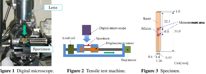
In this study, measurement of displacement and strain fields near interface of bonded structure is carried out based on digital image correlation method using brightness value on material surface. Digital image correlation method is frequently used to measure displacement and strain fields experimentally [1], [2]. Brightness value is obtained by image analysis for material surface image, and surface image is taken by digital microscope (See Figure 1.). In this method, two types surface image have to be prepared to calculate displacement field. One is surface image at before deformation, and the other is that at after deformation. To obtain surface image at before and after deformations, tensile test machine shown in Figure 2 is employed. In this study, specimen shown in Figure 3 is used, and displacement and strain fields near interface at vertex of silicon plate are measured. Each measurement area is singularity field, and it is considered that strain and stress distribution are drastically varied [3]. It is difficult to find report in which singularity field near interface of bonded structure is discussed based on experimental results.
Therefore, in this study, investigation for singularity field near interface of bonded structure is carried out based on digital correlation method.
Figure 1 Digital microscope. Figure 2 Tensile test machine. Figure 3 Specimen.
Acknowledgement
This work was supported by "Program for High Reliable Materials Designand Manufacturing in Nagaoka University of Technology" and Grants-in-Aid for scientific Research(B) Grant Number 90143693.
References
[1] M. Oka, S. Kawahara, T. Ikeda, N. Miyazaki, Improvement of the Accuracy of the Nonlinear Finite Element Analyses for a New 3D SIC Package Using the Thermal Strain Measurement with the Digital Image Correlation, Proceedings of The 13th International Conference on Electronic Materials and
Packaging(EMAP2011) ,pp.1-6(EMAP2011FP-41), 2011.
[2] K. Matsuda, T. Ikeda, N. Shishido, N. Miyazaki, Evaluation of Warpage and Residual Stress in Semiconductor Chips Caused by the Combination of Materials in Packages, Proceedings of The 13th International Conference on Electronic Materials and Packaging(EMAP2011) ,pp.1-8(EMAP2011FP-60), 2011.
[3] M. Kasai, H. Koguchi, T. Kurahashi, Strain singular field near the edge of interface in material with cuboidal inclusion based on experiment and numerical analysis , The 13th International Conference on Electronic Materials and Packaging(EMAP2011), pp.1-10(EMAP2011FP-55), 2011.
Lens
Specimen