Graduate School of Science and Technology
Gunma University
DESIGN OF GRAY CODE INPUT DAC
FOR GLITCH REDUCTION IN
COMPARISON WITH R-2R LADDER
DAC
By Gopal Adhikari
Masters in Electronics, Information and
Mathematics Education Program
Design of Gray Code Input DAC for Glitch
Reduction in Comparison with R-2R
Ladder DAC
A Dissertation Submitted to the
Graduate School of Science and Technology
Gunma University
As a Fulfillment of Thesis Requirement
for the Masters in Electronics, Information and Mathematics
Education Program
By
Gopal Adhikari
Gunma University
Department of Science and Technology
2017
Declaration
I hereby declare that the thesis entitled “Design of Gray Code Input DAC for Glitch Reduction
in Comparison with R-2R Ladder DAC” has been carried out in Gunma University, Faculty of
Science and Technology, Division of Electronics and Informatics, Kobayashi Laboratory. The work is original and has not been submitted in part or full by me for any degree or diploma at any other University. I further declare that the material obtained from other sources has been duly acknowledged in the thesis.
Gopal Adhikari Gunma University
Department of Science and Technology 2017
Gunma University
Department of Science and Technology
Certificate
It is certified that the work reported in this thesis entitled “Design of Gray Code Input DAC for
Glitch Reduction in Comparison with R-2R Ladder DAC” by Gopal Adhikari, has been carried
out under my supervision and is not submitted elsewhere for a degree.
---
Date
---
Supervisor
Professor Haruo Kobayashi Gunma University
Graduate School of Science and Engineering Department of Electronic, Information and
Gunma University
Department of Science and Technology
Approval
This is to certify that the thesis entitled “Design of Gray Code Input DAC for Glitch Reduction
in Comparison with R-2R Ladder DAC” written by Gopal Adhikari has been approved by the
thesis advisor, and further approved by the Board of Examiners as one of the requirements for the completion of Masters in Electronics, Information and Mathematics Education Program, Gunma University. This dissertation complies with the regulation of the University and meets the accepted requirements with respect to originality.
Signed and Approved by the Board of Examiners
_________________________________ Examiner
Professor Yasushi YUMINAKA
_________________________________ Date
_________________________________ Examiner
Professor Tadashi ITO
_________________________________ Date
_________________________________ Supervisor
Professor Haruo KOBAYASHI
_________________________________ Date
Acknowledgements
Occasionally in life there are those moments of unutterable fulfilment which cannot be completely explained by those symbols called words. Their meanings can only be articulated by the inaudible language of the heart.
-Martin Luther King, Jr. hen this thesis has been completed, many individuals have contributed to this work towards its success. Although the space allocated to acknowledge the help and suggestions from supervisors and colleagues is only about a small part of the entire thesis, the impact of their work has been much larger.
I am very much indebted to Professor Haruo Kobayashi for his deep engagement in this work. He supported me throughout my research work with his patience and immense knowledge. He even provided various materials and new ideas regarding analog circuit design. I would also like to take chance to acknowledge Prof. Yasushi Yuminaka and Prof. Tadashi Ito for examining my document and approving for publications.
I cannot remain without acknowledging my colleagues, Mr. Junya Kojima, Mr. Keita Kurihara and other lab members for helping with my research. Mr. Kojima helped me learn simulation software and provided me ideas in designing circuits. Mr. Kurihara and other lab members helped me with translating Japanese language and various other tasks. Moreover, their friendship made the time at the institute much more pleasant.
I am very grateful to my brother, Mr. Khem Raj Adhikari for providing me a chance to continue my studies in Japan. Without him, I would not be able to study in Gunma University, and thus set ground to this thesis.
I would like to take a chance to thank my wife Ms. Pooja Niroula Adhikari for encouraging me in every other things. On top of this, she was always there when I needed comfort, and giving someone a smile is often more important than technical advice. Last but not the least, I would like to thank all other people who were directly or indirectly involved with this research work.
Gunma University, 2017 Gopal Adhikari
Abstract
his dissertation deals with a technique to reduce glitches in digital-to-analog converters. It is well known that frequently used R-2R ladder DACs are prone to glitches. R-2R DACs use binary code as their input. Binary code DACs trigger multiple switches at one time for 1-LSB change. This is the reason for occurrence of glitch. Although, a reconstruction analog filter usually follows DAC, it comes with a disadvantage of taking larger chip area in an IC, and/or it requires more components and hence increases the cost. In addition, complete elimination of glitches is very difficult. So, techniques to reduce glitches should be implemented especially for the high-speed DAC. Here, we purpose a DAC which does not require extra space in IC, the number of components as well as the cost of implementation is reduced along with eliminating the glitches (within a simple circuit) that are thought to occur
One candidate as glitch reduction technique is using Gray code [1], which uses only one switch transition at one time for 1-LSB change. However, it has been considered that Gray code input DAC is difficult to realize efficiently and systematically. In fact only one patent [1] has been registered and it has already been expired. Here we take the challenge to develop some topologies for the Gray code input DAC, using the characteristics that binary and Gray codes can be converted to each other using exclusive OR operation.
This thesis also attempts to compare the R-2R DAC and Gray code DAC in terms of their glitch performance. Two topologies (Current Steering Mode and Voltage Mode) of R-2R DACs are compared to corresponding two topologies of Gray code DACs. All the DACs are designed using MOSFETs, and their operation with glitch behaviour was confirmed with SPICE simulation. It was found that the glitches occur due to the multiple switch transition. This happens only in case of the binary code input DAC and not in case of the Gray code input DAC.
Contents
Declaration... i Certificate ... ii Approval ... iii Acknowledgements ... iv Abstract ... v 1 Introduction ... 1 1.1 Thesis Organization ... 22 Digital to Analog Converter Overview ... 3
2.1 Types of Digital to Analog Converters ... 4
2.1.1 The Pulse Width Modulator ... 4
2.1.2 Oversampling DAC ... 4
2.1.3 The Binary Weighted DAC ... 4
2.1.4 The R-2R Ladder DAC ... 5
2.1.5 The Segmented DAC ... 5
2.1.6 Hybrid DACs ... 6 2.2 Specifications of DAC ... 6 2.2.1 Resolution: ... 6 2.2.2 Accuracy: ... 6 2.2.3 Stability: ... 6 2.2.4 Linearity: ... 6 2.2.5 Monotonicity: ... 7 2.2.6 Settling time: ... 7 2.2.7 Speed ... 8 2.3 Errors in DAC ... 8 2.3.1 Offset Error ... 8 2.3.2 Gain Error ... 8 2.3.3 Differential Non-Linearity ... 9 2.3.4 Integral Non-Linearity ... 9 2.3.5 Glitches ... 10
3 DAC Building Blocks ... 11
3.1 Two Stage OPAMP ... 11
3.1.1 Design specifications and design procedure ... 13
3.1.2 Simulation Results... 14
3.3 Binary to Gray Code Converter ... 16
3.4 Current Sources and Sinks... 17
3.5 Bandgap Voltage Reference ... 19
3.5.1 CTAT Circuit Design ... 20
3.5.2 PTAT Circuit Design ... 20
3.5.3 BGR Design ... 22
3.5.4 Simulation Results of BGR ... 22
3.5.5 Start-up Circuits for Current Mirror Based BGR ... 23
3.6 Source Followers ... 24
3.6.1 Simple Source Follower ... 24
3.6.2 Flipped Voltage Follower and Folded Flipped Voltage Follower ... 25
4 R-2R Ladder DAC ... 28
4.1 Voltage Mode R-2R DAC ... 28
4.2 MOSFET Only Voltage Mode R-2R DAC ... 30
4.3 Current Mode R-2R DAC ... 32
4.4 MOSFET Only Current Mode R-2R DAC ... 33
5 Purposed Gray Code Input DAC Architectures ... 37
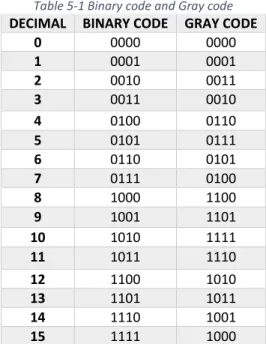
5.1 Number system ... 37
5.1.1 Binary Number system ... 37
5.1.2 Gray Code ... 38
5.2 Glitches... 39
5.3 Gray Code Input DAC Architecture ... 40
5.3.1 Voltage Mode Gray Code Input DAC (VMGCI DAC) ... 41
5.3.2 MOSFET Only VMGCI DAC ... 44
5.3.3 Current Mode Gray code Input DAC (CMGCI DAC) ... 46
5.3.4 MOSFET Only CMGCI DAC ... 50
6 Glitch Analysis of VMGCI DAC in case of sinusoidal signals ... 52
7 Conclusion and Future works ... 59
Bibliography
List of abbreviations Appendix
List of Figures
Figure 1-1 Basic Overview of Signal Processing System 1 Figure 2-1 Block Diagram of Digital to Analog Converter 3
Figure 2-2 Pulse Width Modulator 4
Figure 2-3 Oversampling DAC 4
Figure 2-4 Binary Weighted DAC 5
Figure 2-5 R-2R ladder DAC 5
Figure 2-6 Segmented DAC 5
Figure 2-7 Linearity 7
Figure 2-8 Monotonicity 7
Figure 2-9 Settling Time 7
Figure 2-10 Offset Error 8
Figure 2-11 Gain Error 8
Figure 2-12 Differential Non-Linearity 9
Figure 2-13 Integral Non-Linearity 9
Figure 2-14 Glitches 10
Figure 3-1 Block Diagram of two stage OPAMP 11 Figure 3-2 Small Signal Model of two stage OPAMP 12
Figure 3-3 Two stage OPAMP Schematics 13
Figure 3-4 AC response of the designed two stage OPAMP 14 Figure 3-5 Current Voltage Switch Matrix (a) Definition (b) Realization (c) Timing Diagram 15 Figure 3-6 MOSFET Implementation of DPDT Switch (a) Construction (b) Timing Waveforms 16 Figure 3-7 The conversion process from Binary to Gray (b) circuit diagram for Binary to Gray code conversion 16 Figure 3-8 Timing Diagram of (a) Binary code (b) Gray code 16 Figure 3-9 Simple MOSFET Current Mirror Circuit 17 Figure 3-10 Simulation Results of Current Mirror 18 Figure 3-11 Current Steering Circuit (a) NMOS (b)PMOS 18 Figure 3-12 Simulation Result of (a) PMOS and (b) NMOS Current Steering Circuit 19
Figure 3-13 Block Diagram of BGR 19
Figure 3-14 PTAT Circuit 21
Figure 3-15 BGR Circuit implementation. 21
Figure 3-16 Simulation results of a BGR Circuit 22 Figure 3-17 Transient simulation of different node voltages of BGR 23 Figure 3-18 Source Follower (a) Circuit Diagram (b) Small signal model 24 Figure 3-19 Simulation Results of Source follower 25 Figure 3-20 Flipped Voltage Follower Circuit 25 Figure 3-21 Simulation results of Flipped Voltage Follower 26 Figure 3-22 Circuit diagram of Folded Flipped Voltage follower 27 Figure 3-23 Simulation results of Folded Flipped Voltage follower 27 Figure 3-24 Transistor and resistor sizes for FVF and FFVF 27
Figure 4-1 Voltage Mode R-2R DAC 28
Figure 4-2 Simulation Results, (a) 4-bit R-2R DAC Output, (b) 8-bit R-2R DAC Output 29 Figure 4-3 (a) Differential Non-Linearity (b) Integral Non-Linearity of Voltage Mode R-2R Ladder DAC 30 Figure 4-4 MOSFET Only Voltage Mode R-2R DAC 30 Figure 4-5 Simulation Results, (a) 4-bit R-2R DAC Output, (b) 8-bit R-2R DAC Output 31 Figure 4-6 (a) Differential Non-Linearity (b) Integral Non-Linearity of Voltage Mode R-2R Ladder DAC 31
Figure 4-7 Current Mode R-2R DAC 32
Figure 4-8 Simulation Results of Current Mode R-2R DAC (a) Current Output (b) Voltage Output 32 Figure 4-9 (a) Differential Non-Linearity (b) Integral Non-Linearity of 4-Bit Current Mode R-2R Ladder DAC 33 Figure 4-10 Current Division Principle Using MOSFETs 34 Figure 4-11 4 bit MOSFET only Current Mode R-2R DAC 35
Figure 4-12 Simulation Results of 4-bit MOSFET only Current Mode R-2R DAC 35
Figure 4-13 DNL and INL of MOSFET only Current Mode R-2R DAC 36 Figure 5-1 (a): Glitch Due to MSB change in R-2R DAC 39
Figure 5-2 Glitches in DAC (a) two lobe Glitch (b) single lobe glitch 40 Figure 5-3 VMGCI DAC Architecture 41
Figure 5-4 Configuration of Ladder Network when Gray Code is 0000 42
Figure 5-5 Configuration of the Ladder Network when Gray Code is 0001 42
Figure 5-6 Configuration of Ladder Network when Gray Code is 0010 42
Figure 5-7 Configuration of Ladder Network when Gray Code is 0100 43
Figure 5-8 Configuration of Ladder Network when Gray Code is 1000 43
Figure 5-9 Simulation Results, (a) 4-bit Gray Code Input DAC (b) 8-bit Gray Code Input 43
Figure 5-10 (a) Differential Non-Linearity (b) Integral Non-Linearity of 4-Bit VMGCI DAC 44
Figure 5-11 Design of MOSFET only VMGCI DAC 45
Figure 5-12 Comparison of Simulation Results of 4-bit Gray Code and 4-bit R-2R DAC 45
Figure 5-13 (a) Differential Non-Linearity and (b) Integral Non-linearity of MOSFET Only VMGCI DAC 46
Figure 5-14 CMGCI DAC 47
Figure 5-15 Configuration of Current Mode DAC for Gray Code Input 0000 47
Figure 5-16 Configuration of CMGCI DAC for Gray Code Input 0001 48
Figure 5-17 Configuration of CMGCI DAC for Gray Code Input 0010 48
Figure 5-18 Configuration of CMGCI DAC for Gray Code Input 0100 48
Figure 5-19 Configuration of CMGCI DAC for Gray Code Input 1111 48
Figure 5-20 Configuration of CMGCI DAC for Gray Code Input 1000 49
Figure 5-21 Simulation Results (a) 4-bit Current Steering Mode Gray Code 50
Figure 5-22 (a) Differential Non-Linearity and (b) Integral Non-linearity of CMGCI DAC 50
Figure 5-23 Simulation Result of MOSFET only CMGCI DAC (a) Current Output (b) Voltage Output 51
Figure 5-24 (a) Differential Non-Linearity and (b) Integral Non-linearity of CMGCI DAC 51
Figure 6-1 Test bench for Sinusoidal response for Gray code and R-2R DAC 52
Figure 6-2 Sinusoidal response of VMGCI DAC and R-2R DAC for 1KHz 53
Figure 6-3 Input frequency of 10kHz 53
Figure 6-4 Input frequency of 100kHz 53
Figure 6-5 Input frequency of 200kHz 54
Figure 6-6 Input frequency of 300kHz 54
Figure 6-7 Input frequency of 500kHz 54
Figure 6-8 Input frequency of 800kHz 54
Figure 6-9 Input frequency of 1MHz 54
Figure 6-10 Input frequency of 10MHz 54
Figure 6-11 Input frequency of 15MHz 55
Figure 6-12 Input frequency of 20MHz 55
Figure 6-13 sampling frequency of 2kHz 55
Figure 6-14 sampling frequency of 5kHz 55
Figure 6-15 sampling frequency of 10kHz 56
Figure 6-16 sampling frequency of 20kHz 56
Figure 6-17 sampling frequency of 100kHz 56
Figure 6-18 sampling frequency of 1MHz 56
Figure 6-19 sampling frequency of 10MHz 56
Figure 6-20 sampling frequency of 50MHz 56
Figure 6-21 Response of VMGCI DAC when the bits are delayed. 57
List of Tables
Table 3-1 Design specifications of a two stage OPAMP 13
Table 3-2 Transistor sizes and Simulated results of two stage OPAMP 15
Table 3-3 Sizes of transistors and resistors for BGR during Simulation 23
Table 3-4 Transistor and resistor sizes for FVF and FFVF 27
Table 4-1 Calculation of DNL and INL for 4-bit Voltage Mode R-2R DAC 29
Table 4-2 Calculation of DNL and INL for MOSFET Only 4-bit Voltage Mode R-2R
DAC 31
Table 4-3 Calculation of DNL and INL for 4-bit Current Mode R-2R DAC 33
Table 4-4 Calculations of DNL and INL for MOSFET only Current Mode R-2R DAC 35
Table 5-1 Binary code and Gray code 38
Table 5-2 Calculations of DNL and INL for VMGCI DAC 44
Table 5-3 calculated values of DNL and INL for MOSFET only VMGCI DAC 46
Table 5-4 The Ideal and simulated outputs of CMGCI DAC with DNL and INL
Calculations 49
1
Introduction
lectronic products have become a vital resource for day-to-day life in todays perspective. We can barely think to manage our daily life without the help of electronic equipment like computers, television, or means of modern telecommunication. Most of these products are digital but the need of analog system is and will still be an important aspect in modern electronic world as the world stays analog in nature. Hence, the data conversion should be performed at various points in electronic systems.
There are two forms of data; digital and analog. Data conversion is the process of changing or converting one form of data in to another form. In today’s digitized world, processing and transmission of digital data has become easy and secure with computers. Most complicated applications or logic can easily be done by the use of digital systems than analog circuits. This encouraged the conversion of analog data to digital form. The processing of data is done in digital form. However, the output has to be in analog form because of the fact that human beings can perceive analog signals comfortably than digital. This encouraged the conversion of digital data to analog form. These conversions require devices that can convert digital signals to analog signals and vice versa. The device that converts digital data in to analog data is called Analog to Digital Converter (ADC) and device that converts digital to analog is called Digital to Analog Converter (DAC).
Figure 1-1 Basic Overview of Signal Processing System
The basic overview of signal processing system is depicted in figure 1-1. Generally, the electronic systems take analog signals as input. Because processing must be done using digital methods, an ADC is required to convert the analog signals into digital equivalents, and a DAC is needed to convert the processed signals back to analog for compatibility with analog devices. The filters eliminate undesired higher frequency components and correct other errors during the signal conversion process.
1.1 Thesis Organization
The thesis is organized as follows:
Chapter 1. Introduction. This chapter describes the basic introduction to DAC.
Chapter 2. Digital to Analog Converter Overview: Overview of different types of DACs,
specifications and Errors associated with DACs
Chapter 3: Describes the design of different building blocks of DAC like OPAMP, current mirror,
switch matrix, code converters, Bandgap Voltage reference and Flipped Voltage follower.
Chapter 4. R-2R Ladder DAC: This chapter describes the two architectures of R-2R Ladder DACs.
Current Mode and Voltage Mode architectures. These architectures are designed and simulated using resistors as well as MOS transistors. This chapter is the base to compare the purposed Gray code DAC architectures.
Chapter 5. Purposed Gray code input DAC. This chapter describes the two purposed architectures
of Gray code input DAC. These architectures are designed and simulated by using passive elements like resistors and current sources as well as MOS Transistors.
Chapter 6: Glitch Analysis of VMGCI DAC in case of sinusoidal signals: Contains simulation of
purposed DAC with different inputs and different configurations.
Chapter 7: Conclusion and future works
2
Digital to Analog Converter Overview
he Digital to Analog Converter (DAC) is an interface between the digital signal processing system and the analog world. It is a device that converts digital signals to analog signals (voltage levels, current levels or electric charge). Since human senses are analog in nature and can only perceive analog signals, the digital signals from the DSP systems should first be converted to the analog form before presentation. For example, if the presentation is in the form of strings of 1s and 0s, only people with high technical knowledge can generate the meaning out of it and is a tedious time consuming task. This is where a DAC comes to play a significant role. A DAC helps the user to interpret the data easily. Therefore, the need of DAC is inevitable.
Figure 2-1 Block Diagram of Digital to Analog Converter
The N-bit DAC takes digital data in the form of Binary code as input and converts it to its corresponding analog output in the form of voltage or current. Basic block diagram of a DAC is shown in Figure 2-1. Here, an input N-bit digital word (b1, b2...bN) has a value Digital Input given by Equation 2.1
𝐷𝑖𝑔𝑖𝑡𝑎𝑙 𝐼𝑛𝑝𝑢𝑡 = 𝐵𝑁−12𝑁−1+ ⋯ + 𝐵121+ 𝐵020
(2.1)
Where, 𝐵𝑁−1 is MSB, 𝐵0 is LSB and they take values of either 1 or 0.
DACs are commonly used in various electronic applications such as music players to convert digital data streams into analog audio signals. They are also used in televisions and mobile phones to convert digital video data into analog video signals, which connect to the screen drivers
to display monochrome or colour images. They find applications in various other signal processing equipment.
2.1 Types of Digital to Analog Converters
The most common types are DACs are;
2.1.1 The Pulse Width Modulator
The pulse width modulator is the simplest of DACs. A stable current (electricity) or voltage is switched into a low pass analog filter with a duration determined by the digital input code. This technique is used for motor speed control and is now commonly used in hi-fi audio systems.
Figure 2-2 Pulse Width Modulator
2.1.2 Oversampling DAC
It is a pulse density conversion technique. A simple 1-bit DAC is often chosen, as it is inherently linear. The DAC is driven with a pulse density modulated signal, created through negative feedback. Most very high resolution DACs (greater than 16 bits) are of this type due to its high linearity and low cost. Speeds of greater than 100 thousand samples per second and resolutions of 24 bits are attainable with Delta-Sigma DACs.
Figure 2-3 Oversampling DAC
2.1.3 The Binary Weighted DAC
It contains resistor or current source for each bit of the DAC connected to a summing point. These precise voltages or currents sum to the correct output value. This is one of the fastest conversion methods but suffers from poor accuracy because of the high precision required for each individual
voltage or current. Such high-precision resistors and current sources are expensive, so this type of converter is usually limited to 8-bit resolution or less.
Figure 2-4 Binary Weighted DAC
2.1.4 The R-2R Ladder DAC
Most commonly used type of DAC. It contains only two values of resistors per bit and a switch. This improves DAC precision due to the ease of producing many equal matched values of resistors or current sources, but lowers conversion speed due to parasitic capacitance.
Figure 2-5 R-2R ladder DAC
2.1.5 The Segmented DAC
The Segmented DAC contains an equal resistor or current source segment for each possible value of DAC output. An 8-bit segmented DAC would have 255 segments, and a 16-bit binary-segmented DAC would have 65,535 segments. This is perhaps the fastest and highest precision DAC architecture but at the expense of high cost.
2.1.6 Hybrid DACs
Hybrid DACs are those using a combination of the above techniques in a single converter. Most DAC integrated circuits are of this type due to the difficulty of getting low cost, high speed and high precision in one device.
2.2 Specifications of DAC
D/A converters are available with wide range of specifications specified by manufacturer. Some of the most important specifications are as follows:
2.2.1 Resolution:
Resolution is defined as the number of different analog output voltage levels that can be provided by a DAC. Or, alternatively resolution is defined as the ratio of a change in output voltage resulting for a change of 1 LSB at the digital input. Simply, the resolution is the value of 1 LSB.
𝑅𝑒𝑠𝑜𝑙𝑢𝑡𝑖𝑜𝑛(𝑉𝑜𝑙𝑡𝑠) =𝑉𝑅𝐸𝐹
2𝑁
(2.2)
Where 𝑽𝑹𝑬𝑭 is the reference voltage, N is the number of input bits.
2.2.2 Accuracy:
Absolute accuracy is the maximum deviation between the actual converter output and the ideal converter output. The relative accuracy is the maximum deviation after the gain and offset errors have been removed. Accuracy is also given in terms of LSB increments or percentage of full-scale voltage.
2.2.3 Stability:
The ability of a DAC to produce a stable output all the time is called stability. The performance of a converter changes with drift in temperature, aging and power supply variations. So all the parameters such as offset, gain, linearity error & monotonicity may change from the values specified in the datasheet. Temperature sensitivity also defines the stability of DAC.
2.2.4 Linearity:
The difference between the desired analog output and the actual output over the full range of expected values. The linearity of a DAC is also defined as the precision or exactness with which
the digital input is converted into analog output. An ideal DAC produces equal increments or step sizes at output for every change in equal increments of binary input.
Figure 2-7 Linearity
2.2.5 Monotonicity:
A Digital to Analog converter is said to be monotonic if the analog output increases for an increase in the digital input. If a DAC has to be monotonic, DNL error should be less than or equal to 1 LSB at each output level [2].
Figure 2-8 Monotonicity
2.2.6 Settling time:
Time required for the output signal to settle within +/- (1/2) LSB of its final value after a given change in input scale. The settling time is limited by slew rate of output amplifier. Ideally, an instantaneous change in analog voltage would occur when a new binary word enters into the DAC.
2.2.7 Speed
Rate of conversion of a single digital input to its analog equivalent. Conversion rate depends on clock speed of input signal and settling time of converter. When the input changes rapidly, the DAC conversion speed must be high.
2.3 Errors in DAC
The different types of errors that occur in DACs are briefly discussed below. The different types of errors include offset error, Gain Error, INL error, DNL error, and glitches.
2.3.1 Offset Error
It is the difference between an ideal and actual DAC output when zero digital code is applied to the input. Offset errors are normally bipolar and often expressed in a DAC data sheet in terms of millivolts.
Figure 2-10 Offset Error
2.3.2 Gain Error
It is the difference between an ideal and actual output when full-scale digital code applied to the input. The gain error strongly depends on VREF stability. Gain error of DAC indicates how well the slope of an actual transfer function matches the slope of the ideal transfer function. Gain error is usually expressed in LSB or as a percent of full-scale range (%FSR), and it can be calibrated out with hardware or in software. Gain error is the full-scale error minus the offset error.
2.3.3 Differential Non-Linearity
DNL (Differential Non-Linearity) shows how much two adjacent code analog values deviate from the ideal 1 LSB step. The end fit method corrects the gain and offset error [3]. So, this method is simple and effective. The DNL is calculated using the equation 2.3. Here actual refers to the simulated values and ideal means the end fit reference line.
𝐷𝑁𝐿(𝑛) = (𝑉𝑜𝑢𝑡(𝑛) − 𝑉𝑜𝑢𝑡(𝑛 − 1))𝑎𝑐𝑡𝑢𝑎𝑙− (𝑉𝑜𝑢𝑡(𝑛) − 𝑉𝑜𝑢𝑡(𝑛 − 1))𝐼𝑑𝑒𝑎𝑙 (2.3)
Figure 2-12 Differential Non-Linearity
2.3.4 Integral Non-Linearity
INL (Integrated Non-Linearity) shows how much the DAC transfer characteristic deviates from an ideal one. The ideal characteristic is usually a straight line; INL shows how much the actual voltage at a given code value differs from that line, in LSBs (1 LSB steps). Figure 2.13 shows an example of INL for a 3-bit DAC. INL is calculated using the equation 2.4.
𝐼𝑁𝐿(𝑛) = 𝑉𝑜𝑢𝑡𝑎𝑐𝑡𝑢𝑎𝑙(𝑛) − 𝑉𝑜𝑢𝑡𝑖𝑑𝑒𝑎𝑙(𝑛) (2.4)
2.3.5 Glitches
Glitches are a limitation at high-speed data transfers. They occur during a transition between two output values, as an undesired output value due to difference in signal propagation delay. For a short period of time a false code could be represented at the output [4]. For example if the code transition is from 0111 to 1000 and if the MSB is switching faster than the LSBs, the code 1111 may be present for a short time. This code represents the maximum value and hence the glitch would be large.
3
DAC Building Blocks
arious analog circuit blocks are required to design a fully functional electronic circuit. For example, current mirror circuits, an OPAMP, switches, a reference voltage generator, etc. The Gray code input DAC also requires some functional blocks like current mirrors, switch matrices, and an OPAMP. This chapter attempts to explain and design some of the circuit blocks required for DACs.
3.1 Two Stage OPAMP
Operational amplifier, abbreviated as OPAMP, is an integral part in most of the analog circuits and systems. The basic OPAMP is a 3-terminal device with two inputs; one of which inverts the phase of the signal, the other preserves the phase, and one output (excluding power supply pins). OPAMP is characterized by very high input impedance, very high bandwidth, very high gain, very low output impedance, low power consumption, very high common mode rejection, etc. The popular and most commonly used architecture of OPAMP is a two stage OPAMP. The basic block diagram of two stage OPAMP is depicted in Figure 3-1.
Figure 3-1 Block Diagram of two stage OPAMP
A two-stage operational amplifier consists of a differential amplifier in the 1st stage followed by a common source amplifier (CSA) in the 2nd stage [5]. Differential amplifier stage is to ensure high gain and CSA stage is to further increase the gain and also provide high voltage swing at the output. It can give a differential voltage or single ended voltage, depending on the configuration at the output which depends on differential input voltage. Single-ended output degrades the output
V
swing of the amplifier. Also the common mode rejection ratio (CMRR) degrades as the symmetry of the circuit is lost.
Figure 3-2 shows the small signal model of two-stage operational amplifier. The first stage differential amplifier is connected to the second stage source follower amplifier by a compensation capacitor Cc.
Figure 3-2 Small Signal Model of two stage OPAMP
The transfer function of the OPAMP is derived using the small signal model.
Determination of Transfer Function 𝑉𝑜𝑢𝑡 𝑉𝑖𝑛
=
𝑉2 𝑉𝑑×
𝑉𝑜 𝑉2(3.1)
Applying KCL at the input node,
𝑉2 1/𝑠𝑐1
+
1 𝑅1+ 𝐺𝑚1𝑉𝑑 +
𝑉2−𝑉𝑜𝑢𝑡 1/𝑠𝐶𝑐 (3.2) 𝑉2=
𝑉𝑜. 𝑠𝐶𝑐.𝑅1−𝐺𝑚1𝑉𝑑.𝑅11+𝑠𝑅1(𝐶1+𝐶𝑐) (3.3) Applying KCL at the output node,𝑉𝑜𝑢𝑡 [𝑠(𝐶2 + 𝐶𝑐) +𝑅21] = 𝑉2(𝑠𝐶𝑐 − 𝑔𝑚2) (3.4) From (3.3) and (3.4) 𝑽𝒐𝒖𝒕 𝑽𝒊𝒏
=
𝑔𝑚1𝑅1𝑔𝑚2𝑅2(1−𝑔𝑚2𝑠𝐶𝑐) 𝑠2[𝑅1𝑅2(𝐶1𝐶2+𝐶1𝐶𝑐+𝐶2𝐶𝑐)]+𝑠[𝑅2(𝐶2+𝐶𝑐)+𝑅1(𝐶1+𝐶𝑐)+𝐶𝑔𝑚1𝑅1𝑅2]+1 (3.5) Determination of poles, Zeroes, and other parameters from the transfer functionAt DC, s=0, so the poles and zero are given by
𝑷𝟏 ≈ 1 𝑔𝑚2. 𝑅2. 𝑅1. 𝐶𝑐, 𝑷𝟐 ≈ 𝑔𝑚2 𝐶2 , 𝒁 ≈ 𝑔𝑚2 𝐶𝑐 ≥ 10 ∙ 𝐺𝐵𝑊
For given specifications of DC Gain 𝐴𝐷𝐶 , Gain Bandwidth 𝐺𝐵𝑊, Slew Rate SR, Phase Margin PM, can be related to the circuit parameters as follows:
DC Gain: 𝐴𝐷𝐶 =𝑔𝑚1𝑅1𝑔𝑚2R2 (3.6) 𝐺𝑎𝑖𝑛 𝐵𝑎𝑛𝑑𝑤𝑖𝑑𝑡ℎ ∶ 𝐺𝐵𝑊 = 𝐴 𝐷𝐶 × 𝑃1 ≈𝑔𝑚1 Cc (3.7) 𝑆𝑙𝑒𝑤 𝑅𝑎𝑡𝑒: 𝑆𝑅 = 𝐼𝑜𝑢𝑡𝐶𝑐 (3.8) 𝑃ℎ𝑎𝑠𝑒 𝑀𝑎𝑟𝑔𝑖𝑛: 𝑃𝑀 = − tan−1 𝐺𝐵𝑊 𝑍 − tan −1 𝐺𝐵𝑊 𝑃1 − 𝑡𝑎𝑛 −1 𝐺𝐵𝑊 𝑃2 (3.9) 𝐶𝑜𝑚𝑝𝑒𝑛𝑠𝑎𝑡𝑖𝑜𝑛 𝐶𝑎𝑝𝑎𝑐𝑖𝑡𝑜𝑟: 𝐶𝑐 ≥ 0.22𝐶𝐿 (3.10)
3.1.1 Design specifications and design procedure
The two-stage OPAMP is designed using the TSMC 0.18 micrometer process. The design parameters and specifications are shown in Table 3.1. The design procedure [6] involves the determination of transistor sizes, gain and other specifications.
Figure 3-3 Two stage OPAMP Schematics Table 3-1 Design specifications of a two stage OPAMP
Design Specifications
Technology TSMC 018um Process
DC Gain ≥60dB
Gain Bandwidth (GBW) 30MHZ
Phase Margin ≥ 60°
Slew Rate ≈ 10𝑉/𝜇𝑆
Input Common Mode Range(ICMR) 1.6 (max) 0.8(min)
Load Capacitance 2pf
Power Dissipation ≤ 300𝜇𝑊
Vdd 1.8V-3.3V
Trans Conductance PMOS Kp 92.75𝑢𝐴/𝑉2 Trans Conductance NMOS Kn 246.79 𝑢𝐴/𝑉2
1. 𝐶𝑐 ≥ 0.22 ∙ 𝐶𝐿 = 0.44𝑝𝑓 ≈ 0.6𝑝𝐹 (3.11)
2. 𝑆𝑙𝑒𝑤 𝑅𝑎𝑡𝑒 = 𝐼5
3. 𝑔𝑚1 = 𝐺𝐵𝑊 ∙ 𝐶𝑐 ∙ 2𝜋 = 113.09𝜇 ≈ 170𝑢 (3.13) (𝑊/𝐿) 1, 2 = 𝑔𝑚1
2
𝜇𝑛𝐶𝑜𝑥∙2𝐼5 = 5.186 ≈ 7 (3.14)
4. For design of M3 and M4
(𝑊/𝐿) 3, 4 =𝜇𝑝𝐶𝑜𝑥∙[𝑉𝐷𝐷−𝐼𝐶𝑀𝑅𝑚𝑎𝑥−𝑉2𝐼𝐷3 𝑡3𝑚𝑎𝑥+𝑉𝑡1𝑚𝑖𝑛] ≈ 14 (3.15) 5. For design of M5 𝑉𝑖𝑛 ≥Vgs1+𝑉dsat 5 =>𝑉dsat 5 =0.1004 (3.16) (𝑊/𝐿) 5 = 2𝐼5 𝜇𝑛𝐶𝑜𝑥∙𝑉dsat 5 2 ≈ 16 (3.17)
6. Design of M6, for 60 Phase Margin, gm6=10gm1
(𝑊𝐿) 6= 𝑔𝑚6 𝑔𝑚4 ∙ ( 𝑊 𝐿)4 ≈ 150 (3.18) 7. Design of M7 𝐼6=(𝑊𝐿) 6/ ( 𝑊 𝐿)4× 𝐼4 = 110𝜇𝐴 (3.19) 𝐼7= (𝑊𝐿) 7/ ( 𝑊 𝐿)5𝐼5 => ( 𝑊 𝐿)7=88 (3.20)
Gain of first stage,
𝐺𝑎𝑖𝑛1 = 𝑔𝑚1(𝑟𝑜1||𝑟𝑜4) =𝑔𝑑𝑠1+𝑔𝑑𝑠4𝑔𝑚1 = 71.8894 (3.21) Gain of second stage,
Gain2 = 𝑔𝑚6 (𝑟𝑜6||𝑟𝑜7) = 𝑔𝑚6
(𝑔𝑑𝑠6+𝑔𝑑𝑠7) = 48.0059 (3.22)
Total gain
Gain (ADC) =20log71.8894+20log 48.0059=70.759
3.1.2 Simulation Results
The simulation results of the OPAMP is shown in Figure 3-4.
Table 3-2 Transistor sizes and Simulated results of two stage OPAMP
Transistors W/L Specifications Simulated
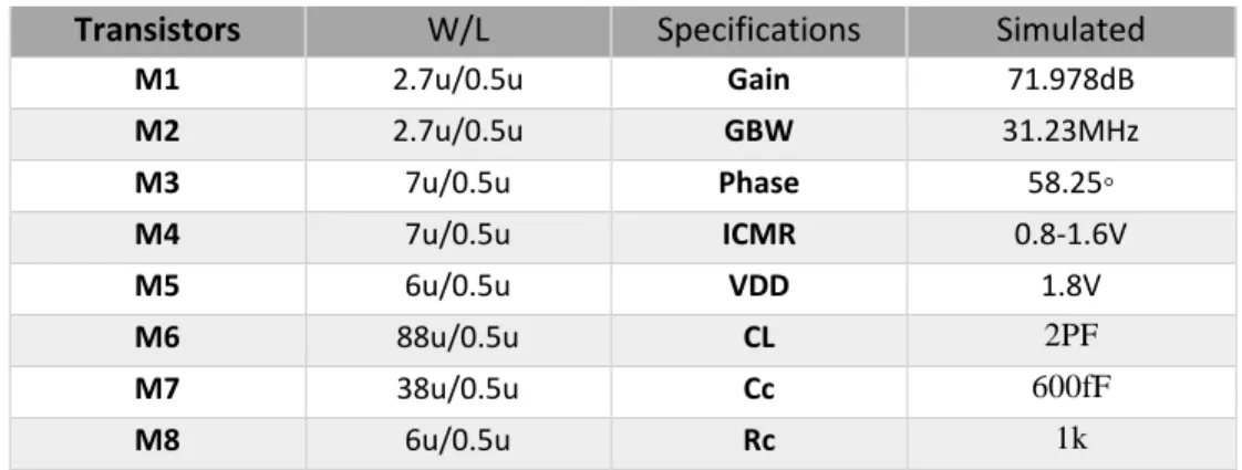
M1 2.7u/0.5u Gain 71.978dB M2 2.7u/0.5u GBW 31.23MHz M3 7u/0.5u Phase 58.25◦ M4 7u/0.5u ICMR 0.8-1.6V M5 6u/0.5u VDD 1.8V M6 88u/0.5u CL 2PF M7 38u/0.5u Cc 600fF M8 6u/0.5u Rc 1k
From the simulated results we can see that the designed OPAMP has met almost all the specifications. Although the phase and GBW trade-off is present in the design as every design does.
3.2 Switch Matrix
The current/voltage switch matrix is a double pole double throw (DPDT) switch, which contains two inputs (IN1 and IN2), two outputs (OUT1, OUT2), and a switch control pin (CTL). The switch connects IN1 to OUT1 and IN2 to OUT2 when CTL is logic LOW. Similarly, it connects IN1 to OUT2, and IN2 to OUT1 when CTL signal is logic HIGH. The CTL pins are provided with Gray code input as generated by circuit in Figure 5-2. The definition, realization and timing diagram of current/voltage switch matrix are shown in figure 3-5 (a), (b) and (c) respectively.
Figure 3-5 Current Voltage Switch Matrix (a) Definition (b) Realization (c) Timing Diagram
These DPDT switches are modelled using NMOS transistors. The transistors’ aspect ratio was used as W/L=2um/0.18um. Figure 3-6 shows the implementation and timing waveforms of MOSFET only DPDT switch for IC implementation.
(a) (b)
Figure 3-6 MOSFET Implementation of DPDT Switch (a) Construction (b) Timing Waveforms
3.3 Binary to Gray Code Converter
Conversion of Binary to Gray code can be realized by using the XOR operation of the binary bits [7]. Binary code: B3, B2, B1, B0, are converted to Gray code: G3, G2, G1, G0 as follows:
𝐺3 = 𝐵3, 𝐺2 = 𝐵3 ⊕ 𝐵2, 𝐺1 = 𝐵2 ⊕ 𝐵1, 𝐺0 = 𝐵1 ⊕ 𝐵0 (3.23) The conversion process and the circuit diagram used for binary to Gray code conversion are shown in Figure 3-7. Also timing diagrams for both binary and Gray codes are depicted in Figure 3-8 (a) and (b).
Figure 3-7 (a) The conversion process from Binary to Gray (b) circuit diagram for Binary to Gray code conversion
3.4 Current Sources and Sinks
A current mirror is a circuit which copies the input current to a current sink or current source as an output current. The principle of the current mirror is that if the gate-source potential of two identical MOSFETs are equal, then the current through these two transistors should be equal [6]. The output current can be identical to the input current or it can be scaled by some factor. It is a basic building block for analog circuits and is used to provide bias currents and voltages to different stages of analog circuits. The current mirror is characterized as:
Output current is linearly related to the input current as 𝐼𝑜𝑢𝑡 = 𝑘 × 𝐼𝑖𝑛
Input resistance is very low Output impedance is very high
A simple current mirror can be constructed using MOSFETs. It requires two identical MOSFETs M1 and M2 where M1 or the input MOSFET is diode connected. And the output is taken from the MOSFET M2. Figure 3-9 shows the circuit diagram of a simple current mirror.
Figure 3-9 Simple MOSFET Current Mirror Circuit
Since M1 is diode-connected, the MOSFET works in the saturation region. The current equation for a diode-connected MOSFET is given in equation 3.24.
𝐼𝑖𝑛 =12𝜇𝑛𝐶𝑜𝑥𝑊1𝐿1 (𝑉𝐺𝑆1− 𝑉𝑇𝐻)2 (3.24)
Assuming the MOSFET M2 is in saturation,
Iout= 12μnCoxW2L2(𝑉𝐺𝑆2− 𝑉𝑇𝐻)2 (3.25)
Dividing equation 3.25 by 3.24, we get Iout Iin = 1 2 μnCoxW2L2 (VGS1− VTH1)2 1 2 μnCoxW1L1 (𝑉𝐺𝑆2− 𝑉𝑇𝐻2)2
If the MOSFETs are matched, i.e. VGS1 = VGS2 and VTH1 = VTH2, then we have Iout Iin = W 2L1 W1L2 ⁄ (3.26) (a) (b) Figure 3-10 Simulation Results of Current Mirror
We know from equation 3.26 that it is possible to replicate the current in input MOSFET to the output if the aspect ratios of the transistors are the same. Also different values of currents can be produced by changing the aspect ratio of the MOSFETs. NMOS current source sinks current to ground, also known as a current sink. PMOS current source sources current from positive supply, hence termed as a current source.
In an integrated circuit, there is often need of multiple current sources and sinks. It is possible to tie up multiple current mirrors to single current source or sink. Multiple current sources or sinks generating from the same reference current is referred as current steering circuit.
(a) (b) Figure 3-11 Current Steering Circuit (a) NMOS (b)PMOS
For example, the reference current is 1µA, and aspect ratio of M1 is 2. We need to generate currents of I1=1µA, I2=2µA, I3=4µA and I4=8µA, then, the aspect ratios of M2, M3, M4 and M5 is calculated as:
(𝑊/𝐿)2= 𝐼1×(𝑊/𝐿)1
𝐼𝑅𝐸𝐹 = 1 ×
2 1= 2
(𝑊/𝐿)3= 𝐼2×(𝑊/𝐿)𝐼 1 𝑅𝐸𝐹 = 2 × 2 1= 4 (𝑊/𝐿)4= 𝐼3×(𝑊/𝐿)1 𝐼𝑅𝐸𝐹 = 4 × 2 1= 8 (𝑊/𝐿)5= 𝐼4×(𝑊/𝐿)1 𝐼𝑅𝐸𝐹 = 8 × 2 1= 16 a b
Figure 3-12 Simulation Result of (a) PMOS and (b) NMOS Current Steering Circuit
3.5 Bandgap Voltage Reference
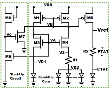
Bandgap voltage generators are widely used in many applications of Analog and Digital Circuits such as LDO (Low Drop Out), Buck/Boost Converters, A/D, D/A, DRAM and flash memories. The low-power and low voltage operations are increasingly in demand for battery operated portable devices. The output generators are designed to stabilize over supply voltage, process and temperature variations. Bandgap voltage reference is a self-biased reference voltage generator that can successfully achieve these requirements. The constant voltage can be generated by combining the PTAT (Proportional to Absolute Temperature) and CTAT (Complementary to Absolute Temperature) [8]. This is the basic idea behind the BGR.
The working principle of BGR Circuits can be illustrated in Figure 3-13. The voltage across the diode has a negative temperature coefficient of about -1.6mV / C also known as the CTAT. The VT has a positive temperature coefficient of about 0.086mV/C also known as PTAT. Since the PTAT is very low in comparison to CTAT so that the PTAT has to be multiplied by some factor to cancel the effect of CTAT to get the constant reference voltage at the output. The reference output voltage can be expressed as
𝑉𝑟𝑒𝑓 = 𝑉𝐷+ 𝐾𝑉𝑇 ……. (3.27)
3.5.1 CTAT Circuit Design
If we pass a constant current Io through a diode, the voltage across the diode is found to be a CTAT. 𝐼𝑜= 𝐼𝑆 𝑒𝑥𝑝𝑉𝐷/𝑉𝑇
𝑉𝐷 = 𝑉𝑇ln𝐼𝐼𝑜
𝑆……. (3.28)
Here 𝑉𝐷 is composed of two terms 𝑉𝑇 = 𝐾𝑇/𝑞 which is a PTAT as it is directly proportional to
temperature.
𝑑𝑉𝑇
𝑑𝑇 = 𝐾
𝑞 (3.29)
The second term ln𝐼𝑜
𝐼𝑆 is a CTAT as 𝐼𝑆 is a CTAT term. This can be verified as follows:
𝐼𝑆 μ. 𝐾. 𝑇. 𝑛𝑖2 (3.30)
μ μ𝑜𝑇𝑚 Where m-3/2
𝑛𝑖 𝑇3𝑒𝑥𝑝−𝐸𝑔/𝐾𝑇 (3.31)
Combining these terms, we have the followings:
𝐼𝑆 𝑇4+𝑚exp−𝐸𝑔𝐾𝑇 (3.32) 𝑑𝐼𝑆 𝑑𝑇 𝐼𝑆( 4+𝑚 𝑇 + 𝐸𝑔 𝐾𝑇2) (3.33) 𝑑𝑉𝐷 𝑑𝑇 (𝑉𝐷−(4+𝑚)𝑉𝑇−𝐸𝑔𝑞) 𝑇 (3.34) 𝑑𝑉𝐷 𝑑𝑇 − 1.88𝑚𝑉 (3.35)
3.5.2 PTAT Circuit Design
Let us consider a circuit as shown in Figure 3-14 to generate a PTAT Voltage. From this figure 𝑉𝐷1= 𝑉𝑇ln𝐼𝐼𝑜
𝑉𝐷2= 𝑉𝑇ln 𝐼𝑜
𝑛𝐼𝑆 (3.37)
𝑉𝐷1− 𝑉𝐷2= 𝑉𝑇ln(𝑛) (3.38) 𝑤ℎ𝑒𝑟𝑒 𝑛 = 𝑛𝑜 𝑜𝑓 𝑑𝑖𝑜𝑑𝑒𝑠.
Figure 3-14 PTAT Circuit
So in order to generate a PTAT circuit, we somehow need to equalize the voltages 𝑉𝐷1 and 𝑉2.
So when,
𝑉𝐷1= 𝑉2 (3.39)
We have the followings:
𝐼𝑜𝑅 = 𝑉𝐷1− 𝑉𝐷2= 𝑉𝑇ln(𝑛) (3.40) This is a PTAT voltage and it is across the resistor R1. So to get a PTAT node, we use the properties of the current mirror as shown in Figure 3-15.
3.5.3 BGR Design
The implementation of PTAT and CTAT is done. Now the BGR is the combination of PTAT and CTAT. Figure 3-15 shows the complete BGR implementation where the PTAT voltage and the CTAT voltage adds together to generate a constant voltage Vref.
𝑉𝑟𝑒𝑓 = 𝛼1∙ 𝑃𝑇𝐴𝑇 + 𝛼2∙ 𝐶𝑇𝐴𝑇 (3.41)
𝑉𝑅2= 𝐼𝑜𝑅2 (3.42)
𝑉𝑅2= 𝑅𝑅2
1 𝑉𝑇ln(𝑛) (3.43)
For Vref to be constant with respect to temperature,
𝜕𝑉𝑟𝑒𝑓 𝜕𝑇 = 0 𝑉𝑅2=𝑅𝑅2 1 𝑉𝑇ln(𝑛) + 𝑉𝐷 (3.44) 𝛼2= 1 𝛼1=𝑅2 𝑅1 ln(𝑛) (3.45) For n=2, 𝑉𝑇 = 26𝑚𝑉, 𝐼𝑜 = 5𝑢, R1=3.6k 𝑅2 =𝛼1∙𝑅1 ln(𝑛) = 97.94𝑘 (3.46)
3.5.4 Simulation Results of BGR
Figure 3-16 (a) shows that Vref is almost constant with respect to temperature, but Figure 3-16 (b) shows that Vref is slightly varying with change in VDD. This can be corrected using the cascode current mirror and the output is shown in Figure 3-16 (c).
Figure 3-16 Simulation results of a BGR Circuit (a) Variation of Different Voltage with change in Temperature (b) Variation of Reference Voltage with change in VDD (c) Stabilization of Reference Voltage employing Cascode Current Mirror
3.5.5 Start-up Circuits for Current Mirror Based BGR
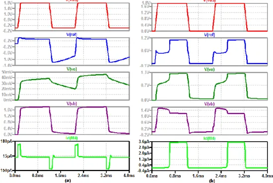
There are conditions in self-biased circuits where the circuit reaches in zero current state. In current mirror based circuit, this state is reached when VA= 0 and VB= VDD (refer Figure 3-15). An NMOS (M7) is connected to VB so when VB reaches to VDD, current starts to flow through M7 pulling VB below VDD. Hence current starts to flow through the mirror. As soon as the current mirror turns on, a big MOSFET M8 starts to conduct pulling VC below VDD. As the VC goes near to zero, M7 turns off, turning off the start-up circuit. The start-up issue is shown in Figure 3-17 (a). Where, the voltage at node VA is 0 and VB is VDD. The waveforms of Figure 3-3-17 (b) verifies the start-up issue being eliminated by using a start-up circuit. Table 3.3 shows the sizes of transistors and resistors during the time of simulation.
Figure 3-17 Transient simulation of different node voltages (a) Before employing Start-up Circuit (b) After employing Start-up Circuit.
Table 3-3 Sizes of transistors and resistors for BGR during Simulation
Transistors Sizes(W/L) M1, M2, M5 5µ/2µ M3, M4 10µ/2µ M6 1µ/2µ M7 2µ/2µ M8 80µ/20µ Resistors R1 5KΩ R2 135KΩ
3.6 Source Followers
The common drain amplifier is also known as the source follower (SF) or the buffer amplifier. The input signal is fed at the gate, and the output is taken from the source terminal. It is also termed as a voltage buffer as its voltage gain is almost equal to 1. It is termed as a source follower because the output voltage closely follows the input. The input resistance is very high and the output resistance is very low. Here some variations of source followers like source follower, flipped and folded flipped voltage followers are discussed and designed in detail.
3.6.1 Simple Source Follower
Figure 3-18 Source Follower (a) Circuit Diagram (b) Small signal model
The body terminal is connected to the lowest supply voltage (ground) to maintain source body junction reverse biased. Since source is connected to output, Vbs changes with output [9]. 𝑉𝑡ℎ= 𝑉𝑡ℎ0+ 𝛾 (√2Φ𝐹+ 𝑉𝑆𝐵− √2Φ𝐹 (3.47) 𝜕𝑉𝑡ℎ 𝜕𝑉𝑖𝑛 = 𝜂 𝜕𝑉𝑂𝑢𝑡 𝜕𝑉𝑖𝑛 (3.48) 𝑉𝑜𝑢𝑡 = 𝐼𝑑 ∗ 𝑅𝑠 =𝜇𝑛𝐶2𝐿𝑜𝑥𝑊[(𝑉𝑖𝑛− 𝑉𝑜𝑢𝑡− 𝑉𝑡ℎ)2] ∗ 𝑅𝑠 (3.49) 𝜕𝑉𝑜𝑢𝑡 𝜕𝑉𝑖𝑛 = 𝜇𝑛𝐶𝑜𝑥𝑊 𝐿 [(𝑉𝑖𝑛− 𝑉𝑜𝑢𝑡− 𝑉𝑡ℎ)(1 − 𝜕𝑉𝑜𝑢𝑡 𝜕𝑉𝑖𝑛 − 𝜕𝑉𝑡ℎ 𝜕𝑉𝑖𝑛)] ∗ 𝑅𝑠 (3.50) 𝑔𝑚 = 𝜇𝑛𝐶𝑜𝑥𝑊 𝐿 [𝑉𝑖𝑛− 𝑉𝑜𝑢𝑡− 𝑉𝑡ℎ] (3.51)
When the Rs is very large, we have the following: Voltage Gain
𝐴
𝑉=
𝑔𝑚𝑅𝑠 1+(𝑔𝑚+𝑔𝑚𝑏)𝑅𝑠≅
𝑔𝑚 𝑔𝑚+𝑔𝑚𝑏=
1 1+𝜂(3.52)
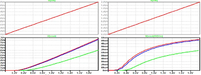
It is evident that the voltage gain (Av) of SF is never equal to 1 even if the value of R1≈ ∞. Here the value of resistor R1 is chosen as 1k 50k and 100k. 𝐼𝐷 depends heavily on the input voltage, introducing nonlinearity in the input output characteristics. So, in order to alleviate this
nonlinearity, the resistance can be replaced by a current source. The circuit of source follower is formed with a load resistance replaced with a simple MOS current source. This current source offers high resistance if it operates in saturation region [5].
Figure 3-19 Simulation Results of Source follower (a) Output voltage for different values of Rs (b) Gain for different values of Rs
3.6.2 Flipped Voltage Follower and Folded Flipped Voltage Follower
The “flipped voltage follower (FVF) [10]” is an enhanced buffer cell widely employed for low-power and/or low voltage operation. The basic FVF cell is a modification of the source follower which gives a more precise copy of the voltage than a traditional source follower. It is basically a two-transistor source follower where the input MOSFET is forced to work at a constant dc current.
Figure 3-20 Flipped Voltage Follower Circuit
M1 and M2 are interconnected as drain to source. Gate of M1 is used as input terminal and its source as output terminal. M3 and M4 form a current mirror. The operating current is supplied by M3 and M4. The mirror current Ix is set by setting the appropriate value of Rx. M1 passes constant
current so that the incremental voltage gain is close to unity. M1 provides shunt feedback and form a two pole negative feedback loop. The output impedance of the control transistor is minimized by the feedback loop [9]. The linear region decreases with increase in Vth. For M1 to provide a constant current, M1 and M2 should be operated in linear region. Conditions for linear region of operation are 𝑉𝐺 ≥ 2√ 2𝐼𝑥 𝜇𝑛𝐶𝑜𝑥(𝑊𝐿)+ 𝑉𝑡ℎ (3.53) And 𝑉𝐺 ≤ √𝜇𝑛𝐶𝑜𝑥(2𝐼𝑥𝑊 𝐿) + 2𝑉𝑡ℎ (3.54) Or, ∆𝑉𝐺 = Vth − √ 2𝐼𝑥 𝜇𝑛𝐶𝑜𝑥(𝑊𝐿) (3.54)
The input and output voltage ranges are very small given by 𝑉𝑡ℎ(𝑀1) − 𝑉𝑑𝑠(𝑀1). It has large sourcing capability thanks to the low output impedance 𝑅𝑜 = 1/𝑔𝑚2𝑔𝑚1𝑟𝑜1. VG may be unacceptably small at smaller values of Ix which causes nonlinearity
Figure 3-21 Simulation results of Flipped Voltage Follower
The direct connection of M1 and M2 of the basic FFV is replaced with a PMOS transistor M3 to form a “folded flipped voltage follower” (FFVF) circuit. The circuit diagram of the folded flipped voltage follower is shown in figure 3-22. M3 is also forced to operate at a constant current Iz. The current through M1 is 𝐼𝑦 − 𝐼𝑧. The function of M3 is to keep the drain-source voltage of M1 constant at the minimum level for saturation. This can be achieved if
√2𝐼𝑧𝛽𝑝+ |𝑉𝑡𝑝| ≥ √2(𝐼𝑦−𝐼𝑧)𝛽𝑛 (3.55)
Figure 3-22 Circuit diagram of Folded Flipped Voltage follower
Figure 3-23 Simulation results of Folded Flipped Voltage follower Table 3-4 Transistor and resistor sizes for FVF and FFVF
Transistors/Resistors Size for FVF (W/L) Size for FFVF (W/L)
M1 10µ/2µ 10µ/0.2µ M2 10µ/2µ 10µ/0.2µ M3 10µ/2µ 10µ/0.2µ M4 10µ/2µ 10µ/0.2µ M5 - 10µ/0.2µ M6 - 10µ/0.2µ Rx 1kΩ 2kΩ Rz - 0.5kΩ
The simulation results show that the FFVF gives increased gain with reduced output resistance in comparison with the FVF.
4
R-2R Ladder DAC
ne of the most common building blocks for a DAC is an R-2R resistor ladder network. It uses only two values of resistors and it is in the ratio of 2:1. For an N-bit ladder DAC, it requires 2N resistors in alternate R and 2R arrangement. The R-2R ladder DAC is very popular because it is easy to design and use less components. However, it is vulnerable to glitches (voltage spikes). There are two ways in which the R-2R DAC can be used, Voltage mode or normal mode, and current mode or inverted mode.
4.1 Voltage Mode R-2R DAC
The R-2R DAC consists of R and 2R resistors, N Switches and an OPAMP. In the voltage mode R-2R ladder DAC, the arms containing 2R resistors are switched between two voltage values namely a reference voltage (VREF), and ground or a lower voltage level (VL). Also its output is taken from the end of the ladder. Since the switches operate between low impedance VREF and ground, so capacitive glitch currents does not flow to the load. The digital input determines whether each resistor is switched to the ground or to the OPAMP [11]. The output voltage is given by:
𝑉𝑜𝑢𝑡 =
𝑉𝑟𝑒𝑓 2𝑏
𝑛−1+
𝑉𝑟𝑒𝑓 22𝑏
𝑛−2+ ⋯ +
𝑉𝑟𝑒𝑓 2𝑛−1𝑏
1+
𝑉𝑟𝑒𝑓 2𝑛𝑏
0(4.1)
Figure 4-1 Voltage Mode R-2R DAC
The advantages of the voltage mode R-2R DAC are
It allows interpolation between any two voltages, none of which must be zero.
Accurate selection and design of R and 2R resistors are possible with simple construction. The resolution can be easily increased by just adding R-2R sections and corresponding
switches.
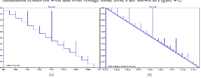
Simulation results for 4-bit and 8-bit voltage mode DACs are shown in Figure 4-2.
.
(a) (b)
Figure 4-2 Simulation Results, (a) 4-bit R-2R DAC Output, (b) 8-bit R-2R DAC Output
The simulation results show that the output is monotonic but contains glitches. The glitch is the largest when the MSB transition occurs.
The ideal and simulated values and calculation of DNL and INL are shown in Table 4-1. The DNL and INL calculations were done using the end-point line fitting algorithm.
Table 4-1 Calculation of DNL and INL for 4-bit Voltage Mode R-2R DAC
BITS SIMULATED IDEAL END POINTS LINE DNL INL GLITCHES(V)
0000 0.00000 0 0.0000000000 - 0.000000000 0 0001 0.19068 0.1875 0.1906153333 0.0000647 0.000064667 0 0010 0.38131 0.375 0.3812306667 0.0000147 0.000079333 0.17859 0011 0.57199 0.5625 0.5718460000 0.0000647 0.000144000 0 0100 0.76250 0.75 0.7624613333 -0.0001053 0.000038667 0.55 0101 0.95317 0.9375 0.9530766667 0.0000547 0.000093333 0 0110 1.14381 1.125 1.1436920000 0.0000247 0.000118000 0.16869 0111 1.33448 1.3125 1.3343073333 0.0000547 0.000172667 0 1000 1.52474 1.5 1.5249226667 -0.0003553 -0.000182667 1.28776 1001 1.71542 1.6875 1.7155380000 0.0000647 -0.000118000 0 1010 1.90605 1.875 1.9061533333 0.0000147 -0.000103333 0.90645 1011 2.09673 2.0625 2.0967686667 0.0000647 -0.000038667 0 1100 2.28724 2.25 2.2873840000 -0.0001053 -0.000144000 0.52526 1101 2.47792 2.4375 2.4779993333 0.0000647 -0.000079333 0 1110 2.66855 2.625 2.6686146667 0.0000147 -0.000064667 0.14395 1111 2.85923 2.8125 2.8592300000 0.0000647 0.000000000 0
(a) (b)
Figure 4-3 (a) Differential Non-Linearity (b) Integral Non-Linearity of Voltage Mode R-2R Ladder DAC
The maximum DNL was found to be 0.000339252 and the minimum DNL was found to be -0.001864138. The maximum INL is 0.000905838 and the minimum INL is calculated to be -0.0009583. DNL and INL plots are shown in Figure 4-3.
4.2 MOSFET Only Voltage Mode R-2R DAC
The voltage mode R-2R DAC was implemented by using MOSFETs only in order to be implemented in IC technology. The switch is a SPST switch and was realized by using two cascaded inverters. The MOSFETs aspect ratio for R and 2R were calculated using equation 4.2.
𝑅 =
𝑉𝐷𝑆 𝐼𝑑𝑆𝐴𝑇=
𝑉𝐷𝑆 𝑢𝑛𝐶𝑜𝑥 2 ×( 𝑊 𝐿)×(𝑉𝐺𝑆−𝑉𝑇𝐻)2(4-2) The aspect ratio for R was calculated to be L=2u
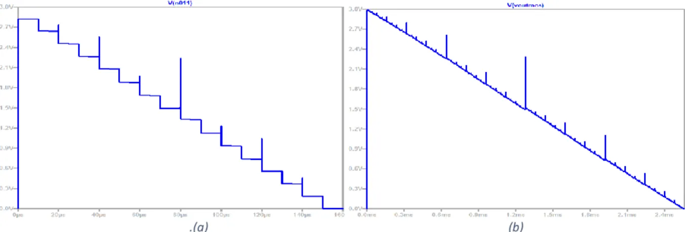
W=1.2u. 2R is just the series combination of two MOSFETs with the values of R. The MOSFETs used for R and 2R are NMOS types. Figure 4-4 shows the schematics of MOSFET only voltage mode R-2R DAC. The 4-bit and 8-bit MOSFET only R-2R DACs were simulated and it was found out that the 8-bit DAC was non-monotonic and both DACs contain glitches. The glitches are due to the difference in switching, and the major glitch that occurs at the midway of the output signal is due to the switching of MSB since all the bits change at this position. So do the switches. Figure 4-5 shows the simulation results of the 4-bit and 8-bit MOSFET only voltage mode R-2R ladder DACs.
-0.00040 -0.00030 -0.00020 -0.00010 0.00000 0.00010 1 3 5 7 9 11 13 15 DNL -0.000300000 -0.000200000 -0.000100000 0.000000000 0.000100000 0.000200000 1 2 3 4 5 6 7 8 9 10 11 12 13 14 15 16 INL
.(a) (b) Figure 4-5 Simulation Results, (a) 4-bit R-2R DAC Output, (b) 8-bit R-2R DAC Output The Table 4.2 shows the DNL and INL calculations for this DAC.
Table 4-2 Calculation of DNL and INL for MOSFET Only 4-bit Voltage Mode R-2R DAC
BITS SIMULATED(VA) IDEAL(VI) END POINTS LINE DNL INL
0000 -6.869329E-07 0 -0.0000006869 - 0.00000000 0001 0.1823497 0.1875 0.1880515122 -0.00570181 -0.00570181 0010 0.36523821 0.375 0.3761037113 -0.00516369 -0.01086550 0011 0.55869652 0.5625 0.5641559105 0.00540611 -0.00545939 0100 0.73513517 0.75 0.7522081096 -0.01161355 -0.01707294 0101 0.9285794 0.9375 0.9402603087 0.00539203 -0.01168091 0110 1.1250138 1.125 1.1283125078 0.00838220 -0.00329871 0111 1.3246123 1.3125 1.3163647070 0.01154630 0.00824759 1000 1.4915565 1.5 1.5044169061 -0.02110800 -0.01286041 1001 1.681682 1.6875 1.6924691052 0.00207330 -0.01078711 1010 1.8751226 1.875 1.8805213044 0.00538840 -0.00539870 1011 2.0738546 2.0625 2.0685735035 0.01067980 0.00528110 1100 2.2613586 2.25 2.2566257026 -0.00054820 0.00473290 1101 2.4481521 2.4375 2.4446779017 -0.00125870 0.00347420 1110 2.6368409 2.625 2.6327301009 0.00063660 0.00411080 1111 2.8207823 2.8125 2.8207823000 -0.00411080 0.00000000
The maximum DNL was found to be 0.01154 and the minimum DNL was found to be -0.021108. The maximum INL is 0.0082475 and the minimum INL is calculated to be -0.01707. The plots of DNL and INL are shown in Figure 4-6.
(a) (b)
Figure 4-6 (a) Differential Non-Linearity (b) Integral Non-Linearity of Voltage Mode R-2R Ladder DAC
-0.03000000 -0.02000000 -0.01000000 0.00000000 0.01000000 0.02000000 1 2 3 4 5 6 7 8 9 10 11 12 13 14 15 16
dnl
-0.02000000 -0.01500000 -0.01000000 -0.00500000 0.00000000 0.00500000 0.01000000 1 2 3 4 5 6 7 8 9 10 11 12 13 14 15 16inl
4.3 Current Mode R-2R DAC
As the name suggests, the current mode DAC operates on the ladder currents. The ladder is formed by R in the series path and 2R in the shunt path. The reference current IREF is divided into i1, i2…..iN in each arm. Currents through 2R resistors are of binary weight relationship. These currents are either diverted to the ground or to the inverting terminal of an OPAMP. The output voltage is given by:
𝑉𝑜𝑢𝑡 = −𝑖
𝑡𝑜𝑡× 𝑅𝑓
(4.3) Where,
𝑖
𝑡𝑜𝑡= ∑
𝐵𝐾×𝑉𝑟𝑒𝑓 2𝑁−𝐾 𝑁−1 𝐾=0×
2𝑅1(4.4)
The advantages of current mode R-2R DACs are
The voltage change across each switch is minimal. So the charge injection is virtually eliminated and the switch driver design is made simpler.
The stray capacitance does not affect the speed of response of the circuit due to constant ladder node voltages. So this improves speed performance.
Figure 4-7 Current Mode R-2R DAC
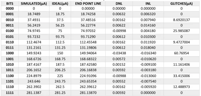
The current steering mode R-2R DAC for 4-bit was simulated, and the simulation results for current output and voltage output are shown in Figure 4-8. Table 4-3 shows the calculation of DNL and INL using the end-point line fitting algorithm.
(a) (b)
Table 4-3 Calculation of DNL and INL for 4-bit Current Mode R-2R DAC
BITS SIMULATED(µA) IDEAL(µA) END POINT LINE DNL INL GLITCHES(µA)
0000 0 0 0.00000 0.00000 0.000000 0 0001 18.7489 18.75 18.74258 0.00632 0.006320 0 0010 37.4931 37.5 37.48516 0.00162 0.007940 8.6920137 0011 56.2419 56.25 56.22774 0.00622 0.014160 0 0100 74.9745 75 74.97032 -0.00998 0.004180 25.985087 0101 93.7232 93.75 93.71290 0.00612 0.010300 0 0110 112.4674 112.5 112.45548 0.00162 0.011920 9.4727004 0111 131.2161 131.25 131.19806 0.00612 0.018040 0 1000 149.9243 150 149.94064 -0.03438 -0.016340 60.76954 1001 168.6726 168.75 168.68322 0.00572 -0.010620 0 1010 187.4167 187.5 187.42580 0.00152 -0.009100 11.161406 1011 206.1652 206.25 206.16838 0.00592 -0.003180 0 1100 224.8979 225 224.91096 -0.00988 -0.013060 33.415006 1101 243.646 243.75 243.65354 0.00552 -0.007540 0 1110 262.3902 262.5 262.39612 0.00162 -0.005920 12.488973 1111 281.1387 281.25 281.13870 0.00592 0.000000 0
The maximum DNL was found to be 0.00632 and the minimum DNL was found to be -0.03438. The maximum INL is 0.01804 and the minimum INL is calculated to be -0.01634. The plots of DNL and INL are shown in Figure 4-9.
(a) (b)
Figure 4-9 (a) Differential Non-Linearity (b) Integral Non-Linearity of 4-Bit Current Mode R-2R Ladder DAC
4.4 MOSFET Only Current Mode R-2R DAC
An important task that has to be performed inside a DAC is accurate weighing of currents, voltages or charges. Typically, passive elements such as resistors and capacitors are used for this purpose because of their linear characteristics. The MOSFETs are inherently non-linear in all the operating
-0.04000 -0.03000 -0.02000 -0.01000 0.00000 0.01000 1 2 3 4 5 6 7 8 9 10111213141516 DNL -0.020000 -0.015000 -0.010000 -0.005000 0.000000 0.005000 0.010000 0.015000 0.020000 1 2 3 4 5 6 7 8 9 10 11 12 13 14 15 16 INL
regions. The R-2R ladder DAC relies on the linearity of the passive elements that divides the input current by the factor of two.
Figure 4-10 Current Division Principle Using MOSFETs
This current division can be accomplished by using MOSFETs despite their non-linear characteristics. The current mode DAC works based on the current division principle. The current division using MOS transistors is shown in the unit cell of the ladder network in Figure 4-10. Here, M1 acts as resistor R. The combination of M2 and M3 or M2 and M4 contributes the resistor 2R. The input current IREF gets divided by M1 and M2 into two parts one part goes through M1 and other goes through M2 [12]. The current in M2 is switched to IOUT by M3 or to IDUMP by M4. M16 and M17 form the terminal 2R resistor. The full 4-bit resolution of MOSFET only R-2R ladder DAC is obtained by cascading this cell as shown in Figure 4-11. The MOSFETs aspect ratio is calculated using the equation 4.5.
𝑅 =
𝑉𝐷𝑆 𝐼𝑑𝑆𝐴𝑇=
𝑉𝐷𝑆 𝑢𝑛𝐶𝑜𝑥 2 ×( 𝑊 𝐿)×(𝑉𝐺𝑆−𝑉𝑇𝐻)2 (4.5) The calculated values of W and L for MOSFETs are 1.29µ and 2.1µ respectively.Figure 4-11 4 bit MOSFET only Current Mode R-2R DAC
The simulation was carried out using VREF=3V and the current and voltage outputs of the MOSFET
only current mode R-2R DAC are shown in Figure 4-12.
(a) (b)
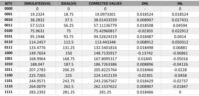
Figure 4-12 Simulation Results of 4-bit MOSFET only Current Mode R-2R DAC (a) Current Output (b) Voltage Output Table 4-4 shows the calculations of DNL and INL for the MOSFET only current mode R-2R DAC.
Table 4-4 Calculations of DNL and INL for MOSFET only Current Mode R-2R DAC
BITS SIMULATED(VA) IDEAL(VI) CORRECTED VALUES DNL INL
0000 0 0 0 - 0 0001 19.2324 18.75 19.0973301 0.018524 0.018524 0010 38.2832 37.5 38.01433559 0.008907 0.027431 0011 57.5153 56.25 57.11136779 0.018508 0.04594 0100 75.9631 75 75.42960817 -0.02303 0.022912 0101 95.1948 93.75 94.52624319 0.018487 0.0414 0110 114.2457 112.5 113.443348 0.008912 0.050312 0111 133.4776 131.25 132.5401816 0.018498 0.06881 1000 149.7654 150 148.7135917 -0.13742 -0.06861 1001 168.9964 168.75 167.8095317 0.01845 -0.05016 1010 188.047 187.5 186.7263386 0.008896 -0.04126 1011 207.2783 206.25 205.8225764 0.018466 -0.0228 1100 225.7265 225 224.1412139 -0.02301 -0.0458 1101 244.9571 243.75 243.2367567 0.018429 -0.02737 1110 264.0079 262.5 262.1537622 0.008907 -0.01847 1111 283.2392 281.25 281.25 0.018466 0
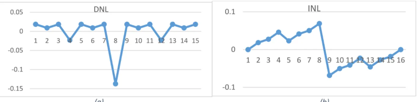
The maximum DNL was found to be 0.018498 and the minimum DNL was found to be -0.13742. The maximum INL is 0.06881and the minimum INL is calculated to be -0.06861. The plots of DNL and INL are shown in Figure 4-13.
(a) (b)
Figure 4-13 (a) Differential Non-Linearity (b) Integral Non-Linearity of MOSFET Only 4-Bit Current Mode R-2R Ladder DAC Here from the above design and calculations, we conclude that the R-2R DAC has decent DNL and INL results. However, these DACs are prone to glitches. The glitches are further increased in higher resolution DACs. This is the main drawback of this type of DACs.
-0.15 -0.1 -0.05 0 0.05 1 2 3 4 5 6 7 8 9 10 11 12 13 14 15 DNL -0.1 0 0.1 1 2 3 4 5 6 7 8 9 10 11 12 13 14 15 16 INL