Density Optimization for Analog
Layout based on Transistor-array
A dissertation submitted for the degree of Doctor of Philosophy in computer system and VLSI design
23 September 2020
Department of Information and Media Engineering The University of Kitakyushu, Japan
Author: Chao Geng (Student ID: 2017DCB401) (Advisor: Shigetoshi Nakatake)
Author’s personal biography and publications are shown on the website ORCID, for more information, please visit the web link https://orcid.org/0000-0002-9637-3922.
I
ABSTRACT
In integrated circuit design of advanced technology nodes, layout density uniformity significantly influences the manufacturability due to the CMP variability. In analog design, especially, designers are suffering from passing the density checking since there are few useful tools. To tackle this issue, we focus on a transistor-array(TA)-style analog layout, and propose a density optimization algorithm consistent with complicated design rules. Based on TA-style, we introduce a density-aware layout format to explicitly control the layout pattern density and provide the mathematical optimization approach. Hence, a design flow incorporating our density optimization can drastically reduce the design time with fewer iterations. In a design case of an OPAMP layout in a 65nm CMOS process, the result demonstrates that the proposed approach achieves more than 48× speed-up compared with conventional manual layout, meanwhile, it shows a good circuit performance in the post-layout simulation.
The main contributions of this paper are listed as follows: 1) To the best of our knowledge, this is the first work handling DRC and layout density simultaneously. We provide a density-aware format for predictability of analog layout density. Besides, the density optimization design flow has great potential for eliminating aggressive dummy-feature-filling-induced problems. 2) We formulate the process to approach the centering value of the density among constraints as a mathematical optimization problem. Furthermore, we provide a reasonable approach to solve the problem, which searches for an optimum by a Min-Dum scheme to avoid exhaustive search on all the feasible solutions, simplifying the problem as a quadratic programming problem. 3) We develop a TA-style analog layout design automation flow incorporating the density optimization, and we demonstrate a design case of an OPAMP layout in a 65nm CMOS process. Compared with a manual layout by the traditional method, the experimental results demonstrate the high efficiency and the effectiveness of our method.
II
Keywords: analog layout, design for manufacturability, layout density, transistor array, algorithm design
III
CONTENTS
ABSTRACT ... I
LIST OF FIGURES ... V
LIST OF TABLES ... VII
CHAPTER 1 INTRODUCTION ... 1
CHAPTER 2 FUNDAMENTAL THEORY ... 4
2.1 Physical Design and Verification ... 5
2.1.1 Dominant EDA Tools Used for Layout ... 10
2.1.2 The Challenges of Today’s IC Layout Design ... 11
2.1.3 DFM Analysis and Verification ... 13
2.2 Density Issue ... 16
2.2.1 CMP (Chemical Mechanical Polishing) ... 18
2.2.2 Investigation for Density Issue Handling ... 22
2.2.3 Layout Density Uniformity ... 28
2.3 Transistor Array ... 30
2.4 Our Proposal to Address Density Issue ... 32
2.4.1 OPAMP Circuit for Design Example ... 35
2.4.2 Parasitic Extraction for Post-layout Simulation . 45
CHAPTER 3 DENSITY-AWARE LAYOUT FORMAT..
... 52
3.1 Density Checking ... 52
3.2 Key Idea ... 53
3.3 Device/pattern parameters for TA-style Layout ... 54
3.4 Density and DRC Constraints ... 56
CHAPTER 4 DENSITY OPTIMIZATION STRATEGY
... 64
4.1 Density Optimization Problem ... 65
IV
4.3 Nonlinear Programming ... 68
CHAPTER 5 DENSITY-AWARE TA-STYLE ANALOG
LAYOUT ... 71
5.1 Feasible Device/Pattern Parameters ... 73
5.2 Optimum Device/Pattern Parameters ... 74
5.3 Design Example ... 76
CHAPTER 6 CONCLUSITON AND FUTURE WORKS
... 90
ACKNOWLEDGEMENTS ... 92
V
LIST OF FIGURES
2.1 Flowchart of IC design………4 2.2 An example of IC layout ………5 2.3 An example of design rules over an analog CMOS layout….6 2.4 An analog CMOS fabrication with respect to its layout
pattern………..8 2.5 Graphical view of density checking in an EDA tool…………10
2.6 Increasing design rules and operations with each process…12
2.7 DRC Plus offers fast 2D pattern matching to find and fix problematic configurations………….………...15
2.8 Lithographic process hotspot verification based on lithography simulation………...15 2.9 Density checking evolvement with the process nodes shrinking………17 2.10 A diagram of the CMP process in VLSI fabrication………..18 2.11 A physical picture of the CMP process in VLSI fabrication……….………19 2.12 Layer stacking of chip in three different cases……….20 2.13 Photo under electron microscope shows post-CMP thickness variation of each layer……….21 2.14 Density variation to the CMP profile………..22 2.15 Density issue handling in digital and analog domains……26 2.16 Dummy fill insertion in a digital layout……….27 2.17 Dummy fill insertion for diffusion layer in an analog layout………..27 2.18 Density variation among neighboring subregions impacts wafer topography………29 2.19 Transistor array……… ..31 2.20 Irregular structures among neighboring transistors lead to post-CMP thickness irregularities………32 2.21 Flowchart of our proposal………..34
VI
2.22 Symbol of OPAMP and its equivalent circuit……….35
2.23 Voltage output swing………..38
2.24 An example of gain of OPAMP with respect to frequency…39 2.25 Frequency response curve of gain against frequency for an OPAMP……….………..41
2.26 Settling time is the time required for an output to reach…44 2.27 Design flowchart of parasitic extraction based on Star-RCXT………..………...…….48
2.28 CCI-based parasitic extraction flow………49
2.29 Post-layout simulation in Virtuoso for the circuit with parasitics………51
3.1 Checking window over the layout………..53
3.2 Density distribution and checking result……….54
3.3 A density-aware layout format of TA-style………..55
3.4 DRC and density constraints in a 65nm CMOS process……61
3.5 Demos to show the layout pattern density controlling……..62
4.1 Density optimization strategy……….64
5.1 Design flow based on the TA layout synthesis……….72
5.2 A flowchart for device/pattern parameters extraction……..76
5.3 OPAMP schematic for a design example………..77
5.4 OPAMP layouts………..79
5.5 Testbench circuits for DC simulation, load capacitance CL is 1.8pF.………..…81
5.6 Testbench circuits for AC simulation, load capacitance CL is 1.8pF………...83
5.7 Testbench circuits for transient simulation, load capacitance CL is 1.8pF……….83
5.8 Post-layout simulation……….86
VII
LIST OF TABLES
3.1 Parameters and annotations used in this work………..63 4.1 Feasible solution set and the corresponding feature density………68 5.1 Summary of design………77 5.2 Design specification and simulation results………84
1
CHAPTER 1
INTRODUCTION
An integrated circuit is fabricated by stacking layers of various materials in a pre-specified sequence, the electrical behavior of circuit depends greatly on the geometrical patterns of the layer [1], [2]. As the IC feature size continues to decrease, the design rules are increased exponentially. However, design period reduction and yield improvement have become more pressing [3], [4]. Chemical Mechanical Polishing (CMP), as a primary technique to control the planeness of silicon surface, is widely utilized in VLSI fabrication [5]. Despite being a predominant planarization technique, CMP is known to suffer from undesired pattern dependent problems [6], [7]. A non-uniform feature density distribution on each layer causes CMP to over/under polish, generating metal dishing and dielectric erosion, which results in the failure of interconnects and yield drop [8].
Previous studies show that post-CMP topography variation is strongly dependent on the underlying feature density, and has become a major cause of yield problem in modern chip manufacturing [9], [10]. For the topography variation reduction and yield improvement, major foundries pay more attention to the layout pattern density. Hence, a rigorous density controlling is imposed to layout design phase so as to achieve uniform topography [11], [12]. However, in the perspective of layout design, rule documentation just indicates layer type which is mandatory to check for density and density level that layout pattern must reach. It cares not for the root-cause or mechanisms behind the density issue. The layout is evaluated as a fine design as long as density meets the required constraints. Therefore, apart from the CMP-directly-relevant layers, such as metals, the layout designer still needs to consider other layers if specified, such as diffusion, poly, and contact.
2
For advanced processes, a minimum and maximum density of a particular layer within a specific area should be specified. Dummy feature filling is a recommended technique by foundries to increase the density of sparse regions, many papers related to filling analysis and synthesis are proposed in past decades [13]-[16]. Density-related research is always a focus in the field of computer-aided design, most of the works consider optimizing the amount of the fills and accelerating the filling process by algorithm [17]-[19]. With respect to dense regions, slotting/removal on the interconnects is applied [20]. However, turnaround time increases due to iterative verification.
Digital circuit often benefits from EDA tools, layer density levels are normally reached with automatic routing. As for analog and RF circuits, gate and metal layers have to be added manually after verification completed. Dummy feature filling is not only error-prone, but also introduces unexpected parasitics to sensitive signals or devices [21], [22]. As reported in the work [23], dummy feature filling may incur problems as technology nodes advance to 65nm and below. Besides, tuning the dimension and position of device layers such as poly, diffusion, metals, contact, to control layout density, is time-consuming and costly. Consequently, the present method to address analog layout density issue is of low efficiency and reliability.
On the other hand, a transistor-array(TA)-style is proposed for analog layout to suppress process-induced variability. The works related to TA-style demonstrate that the circuit performance is not deteriorated even when introducing unit transistor decomposition [24], [25], [26]. Based on the mechanism of density check, we propose a novel scheme where checking window is portioned into identical tiles. A verification-passed transistor-array is assigned into the tile, and then to cover a given layout area by tiles. Thus, any region can pass density check while moving window inspects layout density levels. A key step is to ensure that the transistor-array meets DRC and density constraints.
In this work, we propose an algorithm which aims at solving DRC and density control simultaneously. Combining two
3
processes results in a design speed-up. We develop a predictive CMP density model, and show that the feature density distribution on each layer can be predicted by calculating the total area of the layer within a tile. In addition, through an effective algorithm, our method can prune some inferior solutions so that optimum solution is obtained for yield improvement. Therefore, the overall efficiency of analog layout design is significantly improved.
The rest of work is organized as follows. Chapter 2 gives the preliminaries regarding the density issue, the layout density uniformity, the density checking and the TA-style layout. In this chapter, we also mention the metrics of OPAMP, and parasitic extraction for post-layout simulation. Chapter 3 formulates density and DRC constraints used in this work. Chapter 4 is devoted to describing the density optimization problem and proposing a method to solve the problem. Chapter 5 demonstrates the overall flow for generating the density-aware TA-style analog layout, and also gives a design example auto-generated by our design method. Chapter 6 concludes this work.
4
CHAPTER 2
FUNDAMENTAL THEORY
As information explosively increases nowadays, electronic equipment such as smartphone, wearable device, and laptop are seen everywhere in people’s daily life. ASICs (application specific integrated circuits) or SoCs (system on chips), as critical components inside those equipment, are massively used with the growth of smart terminals in global market. Predictably, in next decade, semiconductor industry will be booming as great needs for chips in emerging technologies, such as, AI (artificial intelligence), big data, cloud computing, automatic driving and smart electronics.
An integrated circuit (IC), sometimes called a chip or microchip, is a semiconductor wafer on which thousands or millions of tiny resistors, capacitors, and transistors are fabricated. From the formulation of specification of circuit to product shipment, the whole flow is extremely complicated and time-consuming. As seen in Figure 2. 1.
5
An IC can function as an amplifier, oscillator, timer, counter, computer memory, or microprocessor. A particular IC is categorized as either linear (analog) or digital, depending on its intended application.
Analog ICs are used as audio-frequency (AF) and radio frequency (RF) amplifiers. The operational amplifier is a common device in these applications.
Digital ICs are used in computers, computer networks, modems, and frequency counters. The fundamental building blocks of digital ICs are logic gates, which work with binary data, that is, signals that have only two different states, called low (logic 0) and high (logic 1).
2.1 Physical Design and Verification
Physical design of integrated circuit, also known as layout design (see Figure 2.1. 1), is to create planar geometric shapes
corresponding to patterns of metal, diffusion, via or other multiple semiconductor layers which make up the device of the integrated circuit. This geometric representation is called integrated circuit layout, after valid layout data is delivered to foundry, the foundry converts the data into another format and use it to generate the photomasks used in a photolithographic process of semiconductor device fabrication [27]-[29].
6
Since final behavior of chip depends largely on the positions and interconnections of the geometric shapes, high-quality layout guarantees that circuit can be turned into chip with excellent performance.
ICs consist of miniaturized electronic components built into an electrical network by photolithography on a monolithic semiconductor substrate. The physical layout of a certain circuit is typically critical to the success. In order to achieve the desired speed of operation, measures are taken such as: to segregate noisy portions of an IC from quiet portions; to balance the effects of heat generation across the IC; or to facilitate the placement of connections to circuitry outside the IC.
When using a standard process to create layout, interaction between interconnect wires and devices must be taken into account. In general, typical effects such as, interaction of the many chemical, thermal, and photographic variables, will be considered and controlled by foundry.
For the manufacturability, layout must be manipulated under design rules to meet certain criteria: performance, size, density, power dissipation. In the design of very-large scale integration (VLSI), massive design rules and constraints are imposed to layout creation, such as minimum space between geometries, interconnects. Minimum or maximum size of polygon shapes. As shown in Figure 2.3.
7
After layout is generated, which needs to be inspected by series of checks, in order to ensure manufacturability and functionality of circuit, this process is called layout verification. Physical verification checks the correctness of the generated layout design. Most common checks in verification process are listed as below. This consists of verifying that the layout:
• Complies with all technology requirements – Design Rule Checking (DRC).
• Is consistent with the original netlist – Layout vs. Schematic (LVS).
• Has no antenna effects – Antenna Rule Checking.
• Passes the density verification at the full chip level. Density error-free is a very critical step in the lower technology nodes (Density Checking).
• Complies with all electrical requirements – Electrical Rule Checking (ERC).
• Guarantees the extra extracted parasitics will still allow the designed circuit to function – Parasitic Extraction. When all of verification is completed, the data is translated into an industry-standard format, typically GDSII, and sent to a semiconductor foundry for fabrication. The process of sending this data to the foundry is called tape-out because the data used to be shipped out on a magnetic tape. The foundry translates it into another format and use it to make photomasks.
8
As shown in Figure 2.4,an analog CMOS layout pattern is transformed into a circuit in silicon wafer.
Figure 2.4: An analog CMOS fabrication with respect to its layout pattern [30].
Each layout pattern layer is formed in silicon wafer by photolithographic technique and all layers are stacked in an order prescribed by foundry. The silicon topography of fabricated circuit is shown by a side view of the figure above.
In the technology process nodes at 65nm and below, to improve the manufacturability and yield of IC chips in advanced process nodes, a rigorous density checking has to be imposed to layout design phase.
Figure 2.5 shows that layout designer inspects locally or globally the density level across a chip, but only few EDA tools provide such advanced graphical view for density checking. The
9
view in Figure 2.5(a) shows the difference in color which distinguishes the density level. Higher density tends to be red while lower density tends to be blue, by which layout designer can better be aware of the density uniformity of a chip. The view in Figure 2.5(b) shows the density distribution across tiles in a layout, by which we can learn the density gradient among neighboring regions.
(a) Figure 2.5: Cont.
10
2.1.1 Dominant EDA Tools Used for Layout
In early layout design before 1970, there were no computing system and the term “software” was not yet invented. The circuits were simple, and the layout was drawn with pencils and rulers, and the physical geometries were checked by eyeballs. With the development of semiconductor technology, the scale of circuit and system become larger, drawing layout by hand was low efficiency and can no longer meet the requirement of the time to market.
As computer technology thrived at next decades, electronic design automation (EDA) tools was developed rapidly with the software technology. For now, mostly used software targeted at modern IC layout are Cadence, Synopsys, Mentor Graphics, as they are dominant among EDA tool vendors. With the aid of IC
(b)
Figure 2.5: Graphical view of density checking in an EDA tool [31]. (a) Density checking in a chip layout. (b) Density distribution across tiles in a layout.
11
software, including place and route tools or schematic-driven layout tools, the speed of design is accelerated significantly.
• Cadence Virtuoso Platform – Tools for designing full-custom integrated circuits, includes schematic entry, custom layout, physical verification, extraction and back-annotation. It is mainly used for analog, mixed-signal, RF, and standard-cell designs.
• Synopsys Design and Verification Platform – Deliver the best silicon chips faster with the world’s No.1 electronic design automation tools and services, industry’s broadest portfolio of high-quality, silicon-proven IP. Major products include Design Compiler, IC Compiler.
• Mentor Graphics Platform – Best-known for its IC verification tool, such as Calibre nmDRC, Calibre nmLVS, Calibre xRC, Calibre xACT 3D, Mentor Graphics company is now acquired by German company Siemens, becoming a part of the Simens PLM software business unit.
2.1.2 The Challenges of Today’s IC Layout Design
Nowadays there are many commercial EDA tools available for accelerating IC design, reducing the period of design. However, as the process node is shrinking, both the size and spacing of design features are decreasing. Besides, as semiconductor technology enters deep sub-micron era, many physical process effects that were relatively insignificant at earlier nodes begins to impact the yield and performance.
Especially, with the shift to nanometer geometries from 65nm to 45nm, design rule compliance no longer guarantee that layouts could be turned into chips as expect. Some unexpected effects may severely affect the electrical characteristics of circuits.
On the other hand, millions of transistors integrated across a die is quite normal at advanced nodes. Since the size of features and spaces between them decrease, interactions of features become more significant and sophisticated.
12
To ensure manufacturability and to control interactions of IC layout, numerous design rules for advanced nodes are imposed to layout creation, they often encompass multiple operations per rule, such as multi-variable equations that express complex spatial constraints and relationships between design features within a certain 2D proximity.
As the integrated circuit feature size continues to decrease, the design rules are increased drastically. As these rules became more numerous and more complex with the process node (see Figure 2.6), the computational complexity of design rule checks (DRCs) and the number of potential violations grew exponentially.
Although commercial EDA tools yet provide powerful features to deal with those problems, it still cannot keep pace with the development of process nodes. Especially for analog circuits, layout creation by hand is major method and few tools provide automated solution for analog IC design, hence making it more time-consuming.
Figure 2.6: Increasing design rules and operations with each process [32]. node.
13
At the same time, analog application is increasing and reflecting strong growth in wireless and sensing technologies. According to a market research, analog circuitry takes up only 20% of the area of today’s modern mixed signal devices, whereas it’s likely to account for as much as 80% of yield loss.
Challenges that IC designers are facing today [33]-[35], are summarized as below.
• Complexity of IC design and verification is increasing. • Physical effects induced by the process variation become
more significant.
• The risk of catastrophic failure during fabrication is increasing and yield is decreasing.
• The conflict between time dissipation and design complexity become inevitable due to poor feature of EDA tools for analog circuit.
• The demands for reducing design time and improving yield in mass production become increasingly urgent.
2.1.3 DFM Analysis and Verification
As the process node moves to nanometer, interactions between features become significantly and physical effects due to process variation severely affect yield. Therefore, the demand for DFM (design for manufacturability) becomes stronger [36]-[39]. To deal with manufacturing issues, foundry impose more performance-driven constraints and yield driven constraints to design rules. On the other hand, in layout design process, EDA vendors develop more powerful tools embedded with DFM-driven features, making IC design more effectively converge in fewer iterations.
There are already some applications and approaches addressing yield issues caused by random effects or fabrication failures. The process-based DFM solutions identify and fix design areas that are easily introduced into design violations. Such as, shorts and opens. Wire spreading, via doubling and critical area analysis becomes mainstream.
14
Some effective technologies to deal with manufacturing issues are introduced below.
• Rule-based DFM. • DRC Plus.
• Model-based DFM. • Variability based DFM.
Rule-based DFM. The design rule is a set of geometrical constraints that define spacing between features and interconnect layers, layout creation is manipulated under the constraint of the design rules. Only configurations that comply with constraints can be fabricated. Design compliance ensure that circuits can work as expect. Even complex issues such as dielectric constant (k), numerical aperture (NA), source frequency (λ), source shape and off-axis illumination, are summarized in the form of geometric measurements such as minimum line width, minimum space, and forbidden pitches. Complex interactions can be defined as specifications on tip-to-tip spacing and tip-to-tip-to-line spacing using DRC. Sufficient design rules can maximize circuit performance and minimize process variation. As the process nodes move to 65nm and below, the mount of the design rules increases dramatically.
In manufacturing process of integrated circuits, some cases always happen that some features can’t be fabricated even if geometries comply with design rules. Designers quickly recognize the limitations of traditional design rules at advanced nodes. Considering this fact, designer augments design rule checks using DRC Plus, which adds fast 2D pattern matching to standard DRC to identify problematic configurations. By this way, designers can quickly fix undesirable geometries. As seen in Figure 2.7.
15
Model-based DFM. This tool predicts manufacturing results by using lithographic simulation, allowing designers to refine and correct layouts before tape-out. It’s effective to identify specific design areas most likely to suffer distortion in the actual manufacturing. EDA vendors provide designers with design kit, much like DRC kit, to run simulation and to get an accurate description of layout creation under given process. Then, hotspots, also called error-prone area, can be identified and revised for the DRC clean. See the Figure 2.8.
Variability based DFM. There is a variation between the silicon shape and drawn layout due to pattern fidelity issues at
Figure 2.7: DRC Plus offers fast 2D pattern matching to find and fix problematic configurations [32].
16
advanced nodes. It will erode performance and cause catastrophic manufacturing failures. Designers must extract variation and bring it into the design flow for analysis, control and minimization. In order to avoid poorly matching silicon behavior of transistors and interconnect layers, variation-based DFM becomes essential to layout design. One example of variation-based DFM is lithography simulation, which predicts silicon shape by utilizing information extracted from layout. Then realistic process-based pattern can be used for chip fabrication. Contour-based extraction uses simulated critical dimensions for transistor gates to extract timing information. With accurate comparison to silicon measurements, an accurate model of current density can be obtained.
As the demand of design for manufacturability is growing, some manufacturing issues that was previously handled during fabrication, now has been pushed up to design and verification stage in the top-down IC design flow. Processed-based simulation provides accurate model for silicon shape, and other techniques enhance verification, which will help improve yield significantly.
2.2 Density Issue
In the process of chip fabrication, there is a step to ensure the planarity of the layer surface, called chemical mechanical polishing (CMP). Since only planar-shape silicon can be manufactured and uniform thickness of dielectric reduce the process variation. In the layout design stage, uniformity of layer is corresponding to planarity of silicon shapes. For the manufacturability, the density of each layer must be inspected under a set of density constraints. Density constraints at each process is provided by foundry. As the process nodes decrease, density checking is evolving progressively. See Figure 2.9 and the following summaries.
17
• Checking area moves from silicon to cell.
• Responsibility for density checking moves from foundry to IP designer (cell designer).
• Density concern moves from manufacturing to design and verification stage.
In technologies before 130nm, to reduce density variation, foundry adds extra metal shapes in the empty spaces without even telling customers. Since the process is thought of having no impact on electrical characteristics of the circuit, dummy fill is nonfunctional circuit, meaning that, it’s not part of the circuit.
However, with each new technology, foundry has to solve massive challenges. In solving those challenges, they have to make comprises that add new design rules. As mentioned above, both the design rules and density rules increase with the process nodes.
Thus, layout is being constrained at very local level, and density checking is being constrained at macro level (density over a small area). A new technology and layer may be more sensitive to variation in the density, thus needing a new rule for allowable density gradient. Each new technology has made density constraints stringent, meanwhile, adding more restrictions on the layout manipulation. Today’s layout design and verification has become a tough work in process-driven design.
18
After 130nm, as the process nodes decrease, fill placement was becoming more aggressive and closer to signal lines. It’s difficult for foundry to convince customer there was no impact on the electrical behavior of their designs. By around 65nm, it was common for designers to control fill placement themselves, using design rule decks and density requirements provided by the foundry. Even down to 45nm, it was still a chip-level issue to be solved at chip assembly.
2.2.1 CMP (Chemical Mechanical Polishing)
Density checking is important to the manufacturability. Studies show that post-CMP topography variation is strongly dependent on the underlying feature density. A uniform layout pattern density contributes to a uniform topography of silicon wafer, so that the electrical performance of the fabricated circuit can be guaranteed. CMP is a primary technique to control the planeness of silicon surface, which is widely utilized in VLSI fabrication. Figure 2.10 shows the whole process.
As seen from the above figure, CMP is comprised of the wafer carrier that the silicon wafer is attached to the wafer carrier, the slurry feeder that provides chemical slurry, and the polishing pad that grinds the surface of silicon wafer.
19
The wafer carrier and the polishing pad are rotating simultaneously, the slurry feeder is dropping chemical slurry when the polishing pad grinds the silicon surface.
The CMP process is realized to remove the unwanted layer with the combination of chemical and mechanical forces. Physical picture of CMP is given in Figure 2.11. In the VLSI manufacturing process, layout pattern is transformed into the circuit in silicon wafer through the photolithography, various materials are then deposited onto the trench etched by the corrosive acid. Metal interconnects are generally softer than the dielectric material, which usually is silicon dioxide. Therefore, metal interconnects are easily removed by mechanical force while dielectric material is removed by chemical slurry.
CMP is a critical step to ensure the manufacturability and functionality correctness of IC chip. A plane silicon surface for each layer contributes to a good profile of stacking layers. As shown in Figure 2.12, layer stacking of chip in the absence of CMP is twisted and deformed, such profile would severely damage the functionality of chip, as a result, decreasing the yield of chip in mass production. Without considering any CMP related defects, layer stacking of chip after CMP process becomes better as the CMP profile is more planar. However, actual post-CMP profile still shows silicon topography variation in the
20
presence of dishing and erosion side effect. Therefore, it is insufficient for planarizing the silicon surface by CMP only. In some cases, density uniformity improvement in layout design phase is necessary for reducing the topography variation.
When enlarging the post-CMP profile in a photo under electron microscope, as shown in Figure 2.13, we can see the thickness variation of each layer. This demonstrates topography variation on silicon wafer still exists. Therefore, despite being a predominant planarization technique, CMP is known to suffer from undesired pattern dependent problems. A non-uniform feature density distribution on each layer causes CMP to over/under polishing, generating metal dishing and dielectric
21
erosion (CMP side effect), which results in the failure of interconnects and yield drop.
Figure 2.13: Photo under electron microscope shows post-CMP thickness variation of each layer [43]. (a) Thickness variation of layer in silicon topography for an analog circuit. (b) Thickness variation of layer in silicon topography for a digital circuit.
(a)
22
2.2.2 Investigation for Density Issue Handling
Chip manufacturing is largely dependent on the features of device and interconnect in deep-submicron technology. The quality of CMP is highly related to the uniformity of density contribution, and a predictable layout is desirable for good CMP performance [44]. The density distribution to affect profile of silicon shape is shown in Figure 2.14.
In general, density requirements provided by foundry is a set of ranges that define maximum and minimum values for each layer. If the density of a layer is over maximum value, there will cause over polishing on the silicon. If the density of a layer is under minimum value, there will cause under polishing on the silicon. Only the density that falls in the range is considered to be safe. The layer types for density checking vary with the technology process and rule documentation provided by the semiconductor foundry.
23
In the technology process node 130nm and above, CMP affects only the back-end-of-line (metal layers). The density rule for the front-end-of-line (diffusion and poly) does not consider for CMP variation. Contact and via layers are not restricted by density rule. Most copper processes employ dual-damascene process and CMP is not done for contact/via layers. With the decreasing process node, those layers previously ignored by density checking, however, are becoming more important, as the effects induced by physical limitation become more significant. It is inevitable to consider the layers required for density checking in rule documentation, regardless of what mechanism they base on. Note that in our research, we consider 5 layers that combine different mechanism resulting in the density variation for layout pattern.
Our research focuses on manufacturability and yield issue arising from layout pattern density. Rule documentation just indicates layer type which is mandatory to check for density and density level that layout pattern must reach. It cares not for the root-cause or mechanisms behind the density issue. Layout is evaluated as a fine design as long as density meets required constraints.
In the technology node 130nm and above, the density rule for layout design is simple and generally, for metal, density control is easily achieved. Advanced technology nodes are requiring even more complex density checking, a basic check for diffusion/poly/metal is mandatory (In our used CMOS process, density checking for contact is also mandatory). We believe that the density rule for diffusion and poly are relevant with CMP variation. Many literatures point out that the density of diffusion and poly affects the CMP quality [46], which in return affects the function of the circuit.
As for poly, just assuming that if a layout has small tiny poly structure far away from other poly structures, this small poly will get etched more than the other poly. Thus, the layout has problem with the uniformity of the surface for the next process step. This isolated poly also can be easily cracked under extreme temperature or voltage.
24
As for diffusion, the CMP process for the STI (shallow trench isolation) has been optimized as a trade-off between junction leakage and transistor leakage (hump effect). When the STI to ACTIVE step is too high, junction leakage happens. When the STI/ACTIVE step is too negative, transistor leakage increases. The STI step uniformity is depending upon the ACTIVE density uniformity. This is why insertion of dummy active areas is mandatory if density constraints as described in the density rule are not reached.
In the advanced 65-nm technology process, it is effective to combine variations arising from different layers. We think that if we only consider metal layers, the density optimization for the yield improvement will become pointless as poly and diffusion can also affect manufacturability. Besides, we introduce a weight parameter into the objective function, in order to distinguish the priority and importance of each layer.
Although in mechanism point of view, CMP is not done for contact/via layers. In the dual-damascene process, trench for metal deposit and hole for contact/via are formed to a combination. However, it still indirectly affects the topography of upper layer to be polished. As advanced manufacturing process requires multiple parallel vias/contacts to ensure reliable connectivity among layers, verifying the existence of sufficient vias/contacts in the layout becomes necessary. In the perspective of manufacturability, we have to take contact (in our work, the density rule requires only check for contact) into account. In designing layout pattern of advanced technology nodes, designers always try to extend the enclosure of the diffusion area when possible, since overlay may make that one contact falls on the border of the diffusion area, thus generating a junction leakage. Designers also follow DFM guideline to double contact and extend poly and metal 1, in order to reduce the electro-migration effect and risk of open circuits. In our objective function, the weight for contact is relatively low compared with other layers, because it has a small impact on the manufacturing of the given pattern. In addition to the consideration of layer type, the handling method for solving the density is also important.
25
To solve high-density problem, there usually takes measures like:
• Ripping up the layout and making spaces between features larger to decrease density.
• Splitting wide interconnect into multiple lines.
• Slotting on the area where the size of feature is large. • Reducing dummy fills or features that have no impact on
electrical behavior of the circuits.
To solve low-density problem, there are many place and route tools available for digital circuits, mainly inserting dummy fills in the empty spaces to increase density. In the past decades, there were many papers in EDA (electronic design automation) domain proposing effective methods to insert dummy fills. At the same time, they still consider parasitic effect like coupling capacitance. Some papers adopt effective algorithms to formulate model based on the CMP process, then to do density analysis by model.
Although they have made great contributions to solve density issue, their methods are just applicable to digital circuits. As for analog circuits, there are few automated tools to provide features for layout design.
As the process nodes decrease, circuits are becoming larger while spaces between features are becoming smaller, the limitations of fill insertion become significant. For instance, in the chip assembling before tape-out. There are density violations in blocks over the layout, however, all blocks are complete, and positions are yet fixed. In this situation, to insert dummy fills is difficult and miserable to designers. Hence, fill insertion seems to have reached its bottleneck at advanced nodes.
Previously, fill insertion was an effective way to solve density issue. But now, it’s reaching to its limitations at advanced nodes. Challenges for now to solve density issue are summarized as following.
26
• Many EDA tools provide powerful features to address density issue, while few options are available for analog layout.
• Fill insertion becomes more aggressive and dummy fill becomes closer to signal lines as the process nodes decrease. • Dummy fills bring unexpected parasitics that significantly
affect the electrical characteristics of the circuit.
• Tuning circuit and redrawing layout for fill insertion severely influence the yield and the time-to-market.
Figure 2.15 shown above summarizes the density handling in digital and analog domains. To compensate the CMP variability and topography variation, layout techniques such as dummy filling for sparse region and slotting/removal on interconnects for dense region are applied to control the layout pattern density.
For the density issue in digital circuits, EDA tool is very convenient to handle the issue, and most of the works consider optimizing the amount of the fills and accelerating the filling process by algorithm. For the density issue in analog circuits, however, layout designers have to handle the issue manually as there are few useful tools.
Herein, we emphasize the drawback of dummy feature filling in analog layouts by using cases of a digital circuit and an analog circuit, respectively.
27
Figure 2.16 shows dummy fill insertion in a digital layout which is a logical module for an ADC (analog-to-digital converter) in a 65nm CMOS process. As seen from the figure, some empty regions in layout are filled up with the metal dummy features, in order to reduce the inter-layer dielectric (ILD) thickness variation. As such, the layout pattern density can be uniform and the silicon topography in each layer can become smooth.
Since an EDA tool provided an efficient way, dummy feature is automatically filled up and density checking is easily passed in just few minutes.
However, in a dummy fill insertion for diffusion layer of an analog layout designed for a low-pass filter in a 65 CMOS process, as shown in Figure 2.17, it spends several days to pass the density checking.
Figure 2.16: Dummy fill insertion in a digital layout.
28
Because in a limited given layout size, there is no more empty space to fill diffusion layer. Meanwhile, analog layout designer needs to calculate the diffusion density that can pass the density checking. Most importantly, the designer has to ensure that manual insertion in resistor array for the diffusion layer does not introduce other DRC violations.
The density checking is finally passed until an appropriate density value is properly calculated and dummy fills are carefully added in empty regions. The experience of dummy fill insertion in an analog layout is really suffering.
In summary, comparisons between the digital and analog circuits are as follows:
• Density-related research is always a focus in the field of computer-aided design (digital circuit).
• Various algorithms provide efficient ways to control layout pattern density (digital circuit).
• Dummy filling is error-prone and introduces unexpected parasitics to sensitive signals or devices (analog circuit). • Tuning the dimension and position of device layers is
time-consuming and costly (analog circuit).
Therefore, the present method to address density issue for analog circuits is of low efficiency and low reliability, providing an efficient approach for analog layout to handle the layout pattern density has a great significance.
2.2.3 Layout Density Uniformity
To improve the CMP quality, layout design must comply with density rules and fill dummy features to restrict the variations on each layer.
Local pattern density within every predefined window must be within a specified range, these density bounds can help in minimizing the multi-layer accumulative effect. However, unbalanced wire distribution still exists even layout pattern density satisfies the constraints. Density variation among neighboring subregions impacts topography, thereby influencing
29
the CMP quality and the yield. Hence, it is not enough to satisfy the density constraints only. Seeking for the minimum wire-density gradient can further improve the yield, which is the objective of our algorithm after-mentioned.
As shown by the example in Figure 2.18, aerial view for layout pattern and lateral view for wafer topography are given respectively. If the density lower and upper bounds are 20% and 80%, respectively. Wafer topography variation is reduced after inserting dummy fills in empty regions, whereas the feature distribution in two subregions can be different even their densities are same (see Figure 2.18(a)). In Figure 2.18(b) and Figure 2.18(c), the four adjacent tiles all satisfy density constraints. However, Figure 2.18(c) is better for CMP control because it has the minimum wire-density gradient. Thus, density uniformity is critical to optimize the yield.
Figure 2.18: Density variation among neighboring subregions impacts wafer topography. (a) Different wire distribution in a subregion exists even under the same density. Large density variation among neighboring subregions leads to post-CMP thickness irregularities. (b) Four adjacent tiles all meet density constraints but result in an unbalanced wire distribution. (c) Reducing density gradient among tiles contributes to uniform topography.
30
2.3 Transistor Array
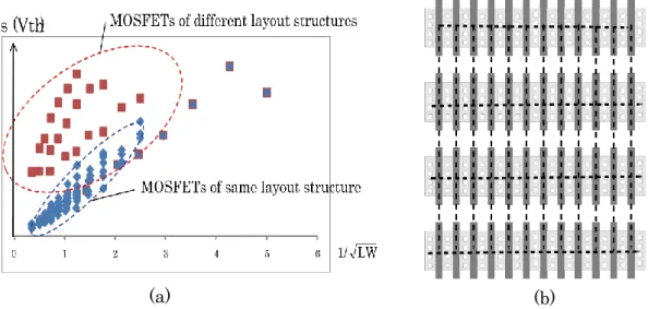
In MOS analog layout, [24] addresses the layout-dependent variability based on the measurement results of test chips on a 90nm CMOS process. As shown in Figure 2.19(a), when increasing the channel size, i.e., L × W, the variation decreases. This is consistent with the Pelgrom model [25].
However, for two transistors with the same channel length and width, if they have different layout structures, the difference of Vth might be bigger than that of the transistors with the same structure. This result reveals that the transistors with unified channel length and channel width can alleviate the layout-dependent variation as expected.
Yang et al. [26] proposes transistor-array(TA)-style for analog layouts. As an extended research of TA, Liu et al. [47] presents a twin-row layout style for transistors-pair with the matching feature and routability.
In TA-style, a large transistor is decomposed into a set of unified sub-transistors, which are connected in series or parallel. Since the transistor decomposition in the channel length direction does not introduce a significant error, all the sub-transistors are then able to be arranged on a uniform grid like an array, thereby obtaining a well-structured layout as illustrated in Figure 2.19(b).
31
With such an array-based structure, a better post CMP profile is expected to be achieved as well [26], and the STI (Shallow Trench Isolation)-stress is evened up.
The works introduced in [24]-[26] clarify that, analyzing the DC/AC measurement results from the test chip, the channel decomposition of the MOS transistor, it does not show too much difference between the decomposed transistor and the original transistor. Therefore, if the design does not require very strict electrical characteristics, the channel decomposition of the MOS transistor, as well as TA-style layout are applicable to analog designs.
Actually, we use a diffusion-shared structure as shown in for layout generation. This structure has also reportedly shown good capability to suppress mismatch in Ids. On the contrary, Irregular structures among neighboring transistors lead to a bad post-CMP profile, and cause uneven STI-stress, as seen in Figure 2.20.
Figure 2.19: Transistor array. (a) The spatial-dependent variation in Vth for the transistors with the same/different layout structures. The boxes of red represent the spatial-dependent variation with different layout structures, and the boxes of blue are with the same structure. (b) Unified transistor array on grid.
32
2.4 Our Proposal to Address Density Issue
Present challenges to solve density issue are summarized as below.
• Many EDA tools provide powerful features to address density issue, while few options are available for analog layout.
• Fill insertion becomes more aggressive and dummy fill becomes closer to signal lines as the process nodes decrease. • Dummy fills bring unexpected parasitics that significantly
affect the electrical characteristics of the circuit.
• Tuning circuit and redrawing layout for fill insertion severely influence the yield and the time-to-market.
Focus on these challenges, this work proposes a method to deal with them.
• Density-aware format enables designers to evaluate and adjust density level earlier, ensuring density predictable and controllable.
• Constraint (DRC and Density)-driven design makes layout highly conform to requirements, reducing iterations for verification.
• TA-style layout enhances the flexibility of design, where layout can be adjusted by changing the array pitch,
Figure 2.20: Irregular structures among neighboring transistors lead to post-CMP thickness irregularities, i.e., a bad post-CMP profile, and cause uneven STI-stress.
33
stretching the poly gates or widening the diffusion of unit-transistors.
In our proposal of this work, a framework dedicated to a fully automated solution for analog IC design, is used to obtain the optimal device/pattern parameters for density optimization and construct a TA-style design flow for analog layout generation.
Based on the transistor array and the density checking procedures in layout verification, we propose to partition a given layout area into identical tiles where a tile is filled up with a transistor array, so that any regions covered by a checking window can pass the density checking.
We then define the device/pattern parameters that describe a density-aware layout format of a transistor array. Then, based on a 65nm CMOS process, we propose a density optimization objective function for a transistor array that is subject to the formulated DRC and density constraints, the objective is for the density uniformity of layout pattern and uniform density gradient among tiles. An efficient mathematical optimization approach is used to simplify the problem and find the optimal device/pattern parameters.
Then, once the optimal parameters are obtained, a TA-style analog layout design flow is proposed, which consists of circuit partition, floorplanning, placement, and routing. The design flow fully conforms to the common layout design flow under consideration of the matching and symmetry constraints.
Finally, layout design examples of full-transistor OPAMP circuit, an automatic layout under the TA-style design flow incorporating with density optimization, and a manual layout by a traditional method, are used to demonstrate the effectiveness of our proposed method.
Post-layout simulation results of both layouts are performed on a Star-RCXT platform, which provides convincing comparison results as it is the industry standard for the silicon-accurate and high-performance parasitic extraction of advanced process technologies.
34
Both layouts are thoroughly compared with respect to the major metrics of the OPAMP circuit, consisting of DC, AC transient performance specifications. Merits and demerits of an automatic layout by our method are discussed sufficiently.
Figure 2.21 showsthe flowchart of our proposal to address the density issue of analog layout. In particular, we emphasize the design example of the analog layout and post-layout simulation steps for demonstrating the effectiveness of our method. The design example used in this research is an operational amplifier (OPAMP).
As the most commonly used circuit in the analog domain, OPAMP is very convenient and suitable for prototypes to demonstrate the feasibility of whole research. Once the whole flow is demonstrated to be feasible, we can progress the research to a higher level where more complicated circuits would be used. The parasitic extraction is performed on Star-RCXT platform, then the netlist files with parasitics are delivered to Cadence, where post-layout simulation is done through Virtuoso. Conclusion and analysis can be drawn by comparing the metrics of both layouts.
35
2.4.1 OPAMP Circuit for Design Example
Operational amplifier, or OPAMP for short, is a basic building block of analogue electric circuits. OPAMP is a DC-coupled high-gain electronic voltage amplifier with differential inputs and, usually, a single-ended output.
An OPAMP generally has three terminals (excluding power supply terminals). One of the inputs is called the inverting input, marked with a negative or “minus” sign (-). The other input is called the non-inverting input, marked with a positive or “plus” sign (+). In this configuration, an OPAMP produces an output potential (relative to circuit ground) that is typically 100,000 times larger than the potential difference between its input terminals. In a linear operational amplifier, as the input stage of an OPAMP is in fact a differential amplifier, the output signal is known as the amplifier’s gain ( -A ) multiplied by the value of the difference ( 𝑉2 − 𝑉1 ) between the two input signals and is depending on the nature of these input and output signals.
Symbol of OPAMP and its equivalent circuit are shown in Figure 2.22. Where 𝑉1 denotes the inverting input and 𝑉2 denotes the non-inverting input. +𝑉𝑠𝑢𝑝𝑝𝑙𝑦 and -𝑉𝑠𝑢𝑝𝑝𝑙𝑦 are power supplies. 𝑍𝑖𝑛 and 𝑍𝑜𝑢𝑡 denotes the input impedance and the output impedance of OPAMP, respectively. The output is denoted by 𝑉𝑜𝑢𝑡.
36
Operational amplifiers have their origins in analog computers, where they are used to perform mathematical operations such as add, subtract, integration and differentiation, in many linear, non-linear, and frequency-dependent circuits.
Due to its versatility, OPAMP is popular as a building block in analog circuits. By using negative feedback, the characteristics of an OPAMP circuit, its gain, input and output impedance, bandwidth, etc. can be determined by external components. The characteristics are nearly independent of temperature coefficients or engineering tolerance in the OPAMP itself. In a vast array of consumer, industrial, and scientific devices, OPAMPs are the most widely used electronics today, circuit designers can configure an OPAMP circuit with negative feedback constituted by resistors, capacitors, or both. The OPAMP circuit is capable of handling signal amplification, filtering, or arithmetic circuit operations described above, it can also be used to form various functional circuits using different resistors and capacitors as well as configurations. Such as differential OPAMP, summing OPAMP, differentiator OPAMP, integrator OPAMP, non-inverting amplifier, inverting amplifier, and voltage follower circuit. In the active filters and analog-to-digital converters (ADCs), OPAMP is employed as well.
An OPAMP CMOS circuit is an essential element in the analog integrated circuits, and therefore is very suitable for a design example of our density optimization for analog layout based on transistor array. Note that in this research, OPAMP circuit is completely constituted by transistors, as we first demonstrate the feasibility of our proposed design flow in a prototyping algorithm and then attempt to improve its generality in the future works.
The complexity of design example would increase by considering the resistor arrays and capacitor arrays. For this research, because the effectiveness of our method is demonstrated by the comparison results of a manual layout and an automatic layout, it is fundamental to understand the various metrics with regard to electrical performance.
37 • Static power dissipation
We first discuss DC power dissipation and explain the calculations for this. The first part of power dissipation is the quiescent power that is dissipated due to quiescent current and supply voltage. By simply multiplying the total supply voltage (+𝑉𝑠 − (−𝑉𝑠)) by the quiescent current 𝐼𝑞, we attain the quiescent power dissipation 𝑃𝑞 by the following formula.
Pq=Iq•(+Vs-(-Vs))
• Input common-mode range (ICMR)
ICMR is a key parameter important for all OPAMP applications in circuits, and it is one of the first terms of which an analog designer thinks. 𝑉𝐼𝐶𝑀 describes a particular voltage level and is defined as the average voltage at the inverting and non-inverting input ports, 𝑉𝑖𝑛− (𝑉1) and 𝑉𝑖𝑛+ (𝑉2). 𝑉𝐼𝐶𝑀 is expressed as follows.
VICM=(Vin++Vin-)/2
In most applications, 𝑉𝑖𝑛+ is very close to 𝑉𝑖𝑛− because closed-loop negative feedback causes one input port to closely track the other such that the difference between two inputs is close to zero. ICMR is defined as a range over which OPAMP circuit can work normally. An OPAMP whose ICMR ranges from 𝑉𝑆𝑆 to 𝑉𝐷𝐷 is called “rail-to-rail input operational amplifier”, meaning an OPAMP with an excellent input signal voltage range.
• Output swing
Under defined operating conditions where the OPAMP still can function correctly, output swing defines how close the OPAMP output can be driven to rail to rail (either power rail: VDD or VSS), as shown in Figure 2.23. To determine the amount of current that the amplifier is sinking or (2.1)
38
sourcing, comparing voltage output swing specifications is the key. The smaller the output circuit current is, the closer the amplifier would swing to the rail. The voltage output swing capability of an OPAMP is dependent on the OPAMP output stage design and the load current.
• Input offset voltage
In the case of the ideal OPAMP, the DC voltage of the 𝑉𝑖𝑛+ and 𝑉𝑖𝑛− terminals match exactly when the input common-mode voltage 𝑉𝐼𝐶𝑀 is 0 V. In reality, however, there are differences in input impedance and input bias current between the input terminals, causing a slight difference in their voltages. This difference called input offset voltage is multiplied by a gain, appearing as an output voltage deviation from the ideal value 0 V. When used in amplifiers of sensors, etc., the input offset voltage of an OPAMP results in an error of sensor detection sensitivity. To keep sensing errors below a specified tolerance level, it is necessary to select an OPAMP with low input offset voltage. The input offset voltage actually reflects the circuit symmetry inside the OPAMP. The better the symmetry is, the smaller the input offset voltage is. Input offset voltage is a very important performance parameter of operational amplifier, especially when it is used in high-precision OPAMP or DC amplifier. The input offset voltage has a certain relationship with the manufacturing process, and the input offset voltage of bipolar process (i.e. the standard silicon process) has a certain relationship with the manufacturing process. The input offset voltage would be larger if the FET is used as the input stage. For
39
precision operational amplifiers, the input offset voltage is generally less than 1mV. Additionally, input offset voltage is parameter associated with temperature.
• DC/Open-loop gain
The main function of an OPAMP is to amplify the input signal and the more open-loop gain it has, the better. When overall feedback is excluded from the circuit, the DC/open-loop gain of an operational amplifier can be obtained. Open-loop gain, in some amplifiers, can be exceedingly high. An ideal OPAMP has infinite open-loop gain. Typically, an OPAMP may have a maximal open-loop gain of around 105.
To achieve the desired performance, the very high open-loop gain of the OPAMP allows a wide range of feedback levels to be applied. Normally, feedback is applied around an amplifier with high open-loop gain so that the effective gain is defined and kept to a desired figure. At a fixed frequency, the open-loop gain can be represented as follows.
AOL= Vout Vin+-V
in-Where, 𝑉𝑖𝑛+ − 𝑉𝑖𝑛− is the voltage difference being applied to the input terminals. The following Figure 2.24 shows the gain of OPAMP with respect to frequency, where 𝑅𝑓 is a feedback resistance and 𝑅𝑖𝑛 is an input resistance.
(2.3)
40 • Phase margin
The phase margin PM is a measure for the stability of a system with feedback. The higher the phase margin, the more stable the system. Capacitive loading will reduce the phase margin. The phase margin (PM) is the difference between the phase lag φ (< 0) and -180°, for an amplifier's output signal (relative to its input) at zero dB gain or output is same as of input. The phase margin PM is expressed as follows.
PM= φ-180°
For example, if the amplifier's open-loop gain crosses 0 dB at a frequency where the phase lag is -135°, then the phase margin of this feedback system is -135° - (-180°) = 45°. In practice, feedback amplifiers must be designed with phase margins substantially in excess of 0°, even though amplifiers with phase margins of, say, 1° are theoretically stable. However, many practical factors can reduce the phase margin below the theoretical minimum. A prime example is when the amplifier's output is connected to a capacitive load. Therefore, operational amplifiers are usually compensated to achieve a minimum phase margin of 45° or above.
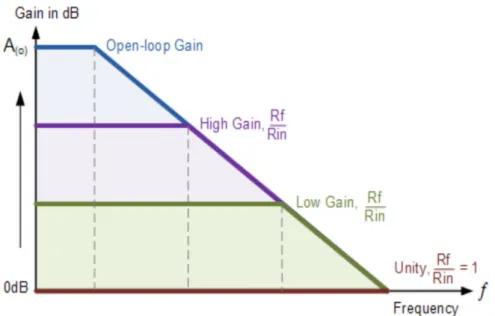
• Gain-bandwidth product (GBP)
The gain-bandwidth product (GBP) for an amplifier is the product of the amplifier's bandwidth and the gain at which the bandwidth is measured. For an amplifier in which negative feedback reduces the gain to below the open-loop gain, the gain–bandwidth product of the closed-loop amplifier will be approximately equal to that of the open-loop amplifier. This quantity is commonly specified for operational amplifier deign, and allows circuit designers to determine the maximum gain that can be extracted from the device for a given frequency (or bandwidth) and vice versa. Figure 2.25 shows the frequency response curve of the product of the gain against frequency, we can see that GBP is constant at any point along the curve.
41
We can also see that the unity gain (0dB) frequency also determines the gain of the amplifier at any point along the curve. Therefore, we have the formula as follows.
GBP= A × BW
Where A is the gain of OPAMP, and BW denotes the bandwidth. For example, from the graph above the gain of the amplifier at 100kHz is given as 20dB or 10, then the gain bandwidth product is calculated as GBP = 106 .
Similarly, the operational amplifiers gain at 1kHz = 60dB or 1000, therefore the GBP is given as GBP = 106. We can
see the results are same.
• Common-mode rejection ratio (CMRR)
The common mode rejection ratio (CMRR) of a differential amplifier (or other device) is a metric used to quantify the ability of the device to reject common-mode signals, i.e. those that appear simultaneously and in-phase on both inputs. The CMRR is the most important specification and it indicates the how much of the common mode signals present to measure. The value of the CMMR frequently depends on the signal frequency and the function should be specified. The function of the CMMR is specifically used to reduce the noise on the transmission lines. An ideal differential amplifier would have infinite CMRR, however this is not achievable in practice. A high CMRR is required
Figure 2.25: Frequency response curve of gain against frequency for an OPAMP.
42
when a differential signal must be amplified in the presence of a possibly large common-mode input, such as strong electromagnetic interference (EMI). An example is audio transmission over balanced line in sound reinforcement or recording. Ideally, a differential amplifier takes the voltages, 𝑉𝑖𝑛+ and 𝑉𝑖𝑛−on its two inputs and produces an output voltage 𝑉𝑜𝑢𝑡 = 𝐴(𝑉𝑖𝑛+ − 𝑉𝑖𝑛−), where A is the differential gain. However, the output of a real differential amplifier is better described as:
Vout= A(Vin+-Vin-)+1
2ACM(Vin++Vin-)
Where ACM is the common-mode gain, which is typically much smaller than the differential gain. The CMRR is defined as the ratio of the differential gain over the common-mode gain, measured in positive decibels. It is expressed by the following formula:
CMRR=20 log10( A
|ACM|)dB
As differential gain should exceed common-mode gain, this will be a positive number, and the higher the better.
• Supply voltage rejection ratio (PSRR)
Supply voltage rejection ratio (PSRR) is defined as the ratio of input offset voltage to supply voltage when OPAMP operates in linear region, which is a term often expressed in decibels. The PSRR reflects the influence of power supply variation on the output of OPAMP, and it is widely used to describe the capability of an electronic circuit to suppress any power supply variations to its output signal. Therefore, the power supply of operational amplifier needs careful treatment when it is used in DC signal processing or small signal processing for analog amplification. Of course, the OPAMP with high CMRR can compensate a part of PSRR. In addition, when using dual power supply, the PSRR of positive and negative power supply may be different. An ideal OPAMP would have infinite PSRR. The output voltage will depend on the feedback circuit, as is the (2.6)

![Figure 2.5: Graphical view of density checking in an EDA tool [31]. (a) Density checking in a chip layout](https://thumb-ap.123doks.com/thumbv2/123deta/8004445.1250266/18.892.267.675.116.595/figure-graphical-view-density-checking-density-checking-layout.webp)
![Figure 2.7: DRC Plus offers fast 2D pattern matching to find and fix problematic configurations [32]](https://thumb-ap.123doks.com/thumbv2/123deta/8004445.1250266/23.892.233.664.136.421/figure-drc-plus-offers-pattern-matching-problematic-configurations.webp)
![Figure 2.10: A diagram of the CMP process in VLSI fabrication [40].](https://thumb-ap.123doks.com/thumbv2/123deta/8004445.1250266/26.892.297.681.628.959/figure-diagram-cmp-process-vlsi-fabrication.webp)
![Figure 2.11: A physical picture of the CMP process in VLSI fabrication [41].](https://thumb-ap.123doks.com/thumbv2/123deta/8004445.1250266/27.892.228.687.508.833/figure-physical-picture-cmp-process-vlsi-fabrication.webp)
![Figure 2.12: Layer stacking of chip in three different cases [42].](https://thumb-ap.123doks.com/thumbv2/123deta/8004445.1250266/28.892.183.769.246.838/figure-layer-stacking-chip-different-cases.webp)