Development of synthetic methods for
bismuth-based oxide and mixed anion compounds
via thin film epitaxy with mist CVD
著者
SUN Zaichun
学位授与機関
Tohoku University
博士論文
Development of synthetic methods
for bismuth-based oxide and mixed anion compounds
via thin film epitaxy with mist CVD
(ミスト
CVD を用いた薄膜エピタキシーによる
ビスマス酸化物・複合アニオン化合物の
合成手法開発)
Zaichun SUN
2020 年
Abstract
Bismuth-based oxides and mixed anion compounds attract much attention as functional materials especially for optoelectronics and solid-state ionic. Among them, metastable β-Bi2O3 with tunnel-like crystal
structure and layered matlockite-type bismuth oxyhalides BiOX (X = Cl, Br, and I) are suitable for photoelectric conversion, because of the highly anisotropic electrical carrier mobility preventing recombination of photo-excited electron and hole pairs and the tunable bandgap to harvest ultraviolet-visible light. Previously, β-Bi2O3
and BiOX have been synthesized in various forms such as polycrystalline powders and nanostructures. However, their epitaxial thin films are highly demanded to investigate their intrinsic properties and device applications. To this end, it is indispensable not only to suppress vaporization of the volatile bismuth and halogens but also to control crystallographic phase and film orientation for β-Bi2O3 and BiOX, respectively. In this study, I developed
facile methods to synthesize high-quality epitaxial thin films of β-Bi2O3 and BiOX.
I synthesized the β-Bi2O3 and BiOX thin films from N,N-dimethylformamide solutions of corresponding
precursors by mist chemical vapor deposition at atmospheric pressure. β-Bi2O3 thin films were grown on α-Al2O3
(0001) and yttria-stabilized zirconia (111) single crystal substrates under N2 gas flow from bismuth (III)
2-ethylhexanoate with a similar coordination state of bismuth to β-Bi2O3. BiOX thin films were grown on
perovskite-type SrTiO3 and (LaAlO3)0.3-(SrAl0.5Ta0.5O3)0.7 (001) single crystal substrates from corresponding
BiX3. O2 fraction in the process gas was controlled by the flow rates of both N2 carrier gas and N2/O2 dilution gas.
Variable growth parameters such as concentration of the precursors, growth temperature and gas flow rates were optimized.
β-Bi2O3 (201) epitaxial thin films with optically flat surface were successfully synthesized at the
optimum growth temperature of 350 °C. The lower and higher growth temperatures resulted in amorphous films and aggregated β-Bi2O3 particles, respectively. From X-ray diffraction and X-ray photoemission spectroscopy, it
was indicated that the epitaxial film was formed via solid phase epitaxy from amorphous intermediates. In addition, short-time post annealing at high temperature was found to be effective to improve the crystallinity and surface flatness.
I also succeeded in synthesis of BiOX (001) epitaxial thin films at the optimum temperature and O2
fraction for each composition. The BiOX epitaxial thin films possessed high crystallinity and atomically flat surfaces. The surface morphology was significantly influenced by the growth temperature. The lower and higher growth temperatures resulted in incomplete coverage and surface roughening of the films, respectively, reflecting the vaporization speed of the solvent and volatile bismuth and halogens. The O2 fraction in the process gas was
crucial to control the oxidation reaction from BiX3 to BiOX, where higher O2 fraction was required for heavier
halogens. It is noted that the lattice constants of BiOCl was tunable via epitaxial strain, enabling to control the electronic structures. The flat surfaces, high crystallinity, and tunable lattice constants would be beneficial for future oxyhalide electronics.
Acknowledgment
I would like to express my deepest appreciation to all those who have helped me during my doctoral research.
Firstly, I would like to express my sincere gratitude to my advisor Prof. Tomoteru Fukumura. His insightful advice, kind research attitude, and constructive suggestions always helped and inspired me to conduct the research. In addition, he always encouraged me thorough the weekly meeting discussion and organized all kinds of parties to make me relaxed. Furthermore, Prof. Fukumura gave me a lot of supports during my daily life in Sendai.
Besides my advisor, I would like to thank Assistant Professor Dr. Daichi Oka. I appreciate all his contributions of patient teachings, creative ideas, and encouragement to make my Ph.D. experience productive and stimulating. Dr. Oka gave me the freedom to pursue my personal research interests. Without his insistent help and guidance, I would have never been able to complete my work.
I also want to thank Dr. Hideyuki Kawasoko and Dr. Kenichi Kaminaga for their useful discussions, guidelines, and warm encouragement. I also want to appreciate Ms. Madoka Suzuki for her support in my daily activities.
Special thanks go to my lab mates: Dr. Amrillah Tahta, Mr. Shintaro Fukuda, Miss Zainab Fatima, Mr. Daichi Saito, Mr. Kyohei Terakado, Mr. Yuki Saba, Mr. Ebube Oyeke, Mr. Noriyuki Ishigane, Mr. Kota Matsumoto, Mr. Taku Yamamoto, Mr. Subaru Yusa, Mr. Nobuto Abe, Mr. Masato Arimitsu, Mr. Mizuki Endo, Mr. Ryosuke Tokunaga, Mr. Naoto Hasegawa, Mr. Yuki Yamamoto, Mr. Masanagi Abe, Mr. Hirokazu Shimizu, Mr. Satoru Miyazaki, Mr. Ryo Azuhata, Mr. Satoshi Sasaki, and Miss Atsumi Hando.
I also acknowledge the scholarship from Ministry of Education, Culture, Sports, and Technology, Japan. Finally, I want to express my profound and deepest sense of gratitude to my parents and my grandparents. Without them, I cannot have the chance to finish my doctoral course.
Zaichun Sun Sendai, Japan
List of abbreviation
Atomic force microscopy: AFM Bismuth oxyhalide: BiOX Chemical vapor deposition: CVD Energy dispersive spectroscopy: EDS Full width at half maximum: FWHM
N,N-dimethylformamide: DMF
One-dimensional: 1D
Reciprocal space mapping: RSM Root mean square: RMS
Scanning electron microscope: SEM Two-dimensional: 2D
Ultraviolet-visible-near-infrared: UV-Vis-NIR X-ray diffraction: XRD
Table of Contents
Abstract ... V Acknowledgment ... VII List of abbreviation ... VIII Table of Contents ... V Chapter 1
General introduction ... - 1 -
1.1 Bismuth-based compounds ... - 1 -
1.2 β-phase Bismuth oxide (β-Bi2O3)... - 1 -
1.2.1 Crystal structure ... - 1 -
1.2.2 Phase stability ... - 3 -
1.2.3 Physical properties ... - 4 -
1.2.4 Synthetic methods ... - 8 -
1.3 Bismuth oxyhalides BiOX (X = Cl, Br, and I) ... - 13 -
1.3.1 Crystal structures... - 13 -
1.3.2 Electronic structure ... - 14 -
1.3.3 Physical properties ... - 17 -
1.3.4 Synthetic methods ... - 21 -
1.4 Overall objective of this study ... - 25 -
Chapter 2 Experimental techniques ... - 27 -
2.1 Mist Chemical Vapor Deposition ... - 27 -
2.3 Crystallographic characterization ... - 33 -
2.3.1 X-ray diffraction ... - 33 -
2.3.2 Raman spectroscopy ... - 35 -
2.3.3 Atomic force microscopy ... - 36 -
2.3.4 Scanning electron microscope ... - 37 -
2.4 Elemental analysis ... - 38 -
2.4.1 X-ray photoemission microscopy ... - 38 -
2.4.2 Energy dispersive spectroscopy ... - 39 -
2.5 Optical properties ... - 40 -
2.5.1 Ultraviolet-visible-near-infrared spectrometer ... - 40 -
Chapter 3 Epitaxial growth of β-Bi2O3 thin Films and particles ... - 41 -
3.1 Experimental method ... - 41 -
3.2 Results and discussion... - 42 -
3.2.1 Growth temperature dependence ... - 42 -
3.2.2 Epitaxial relationship ... - 48 -
3.2.3 Investigation on crystal growth mechanism ... - 49 -
3.2.4 Optimization of the quality of β-Bi2O3 epitaxial thin film ... - 51 -
3.2.5 Thermal stability of β-Bi2O3 ... - 56 -
3.2.6 Optical absorption ... - 57 -
3.3 Conclusions ... - 58 -
Chapter 4 Epitaxial growth of bismuth oxyhalides thin films ... - 59 -
4.1 Experimental method ... - 59 -
4.2.2 Temperature dependence on the epitaxial growth of BiOX thin films ... - 62 -
4.2.3 Composition analysis of the epitaxial growth of BiOX thin films ... - 68 -
4.2.4 Applicability of the growth method on other substrates ... - 70 -
4.2.5 Strain engineering of BiOX epitaxial thin films ... - 72 -
4.2.6 Optical absorption ... - 74 -
4.3 Conclusion ... - 75 -
Chapter 5 Conclusion ... - 76 -
Chapter 1
General introduction
1.1 Bismuth-based compounds
Bismuth is a heavy element with the atomic number 83 belonging to group 15 (pnictides) and possesses [Xe]4f145d106s26p3 electronic configuration. Although bismuth is counted as one of the rare metals, it is commonly
obtained as by-product in other metals and is therefore not very expensive. Besides, bismuth is known to be harmless despite its similar properties with lead, leading to applications such as solders, cosmetics, and medicines as a “green element”.1
The most stable oxidation state of bismuth is Bi3+ with the closed shell electronic configuration of
[Xe]4f145d106s2, forming ionic crystals with other elements such as oxygen and halogens. Because bismuth ions
tend to form chemical bonding with high covalency, asymmetrical coordination is favored by the 6s2 lone pair
electrons hybridized with other orbitals, such as the empty 6p ones, leading to anisotropic crystal structures.2 As
a result, Bi-based ionic crystals like oxides and related materials show characteristic physical properties such as multiferroicity,3 superconductivity,4,5 high ionic conductivity6, photocatalysis and photovoltaics.7–9
This chapter reviews the crystal structure, chemical and physical properties, and synthetic methods reported for β-phase bismuth oxide and bismuth oxyhalides (BiOX, X = Cl, Br, and I), which are representative bismuth-based functional ionic crystals and main targets of this study.
1.2 β-phase Bismuth oxide (β-Bi
2O
3)
1.2.1 Crystal structure
Bismuth oxide (Bi2O3) possesses a characteristic polymorphism as a result of multiple types of
combinations of the asymmetric Bi-O coordination (Figure 1.1).2 Up till now, at least seven polymorphs (α, β, γ,
δ, ɛ, ω, and 𝜂) have been reported.10 Table 1.1 summarizes the crystal structure of Bi2O3. Among the seven
polymorphs, β-Bi2O3 possesses a tunnel-like tetragonal crystal structure similar to the ordered superstructure of
d-Bi2O3 possesses a defect CaF2-based structure, where bismuth atoms occupy the face-centered cubic sites, and
oxygen atoms occupy the simple cubic anion sublattice (32f site) with two sites of oxygen vacancy.11
Table 1.1 Crystal structure of Bi2O3
Phase Point group a (Å) b (Å) c (Å) α (º) β (º) Reference α-Bi2O3 P21/c 5.844 8.157 7.503 90 112.89 12 β-Bi2O3 P4#21c 7.74 7.74 5.665 90 90 13 d-Bi2O3 Fm3m 5.525 5.525 5.525 90 90 14 γ-Bi2O3 I23 10.267 10.267 10.267 90 90 15 ω-Bi2O3 P-1 (2) 8.639 11.97 7.269 93.23 93.35 16 η-Bi2O3 P3m1 3.878 3.878 6.303 90 120 17 ε-Bi2O3 Pnaa 4.956 5.585 12.73 90 90 18
Figure 1.1 Crystal structure of (a) β-, (b) d-, (c) α-, and (d) γ-Bi2O3. All the crystal structures in this thesis were
1.2.2 Phase stability
The phase stability of Bi2O3 was postulated from the differential thermal analysis and high-temperature
X-ray experiments.20 Figure 1.2 shows the phase stabilities of α-, β-, γ-, δ-Bi2O3, and the liquidous phase as
functions of temperature. While α-and δ-Bi2O3 are the most stable phases above and below 730 ºC, β- and γ-Bi2O3
are metastable at any temperature. Scheme 1.1 shows the transformation temperatures for α-, β-, γ-, δ-, and ɛ-Bi2O3. If the supercooling of high-temperature d-Bi2O3 occurs, β-Bi2O3 can be formed between 645 and 650 °C.
β-Bi2O3 transforms back to d-Bi2O3 by annealing at over 670 °C. During the cooling process to room temperature,
β-Bi2O3 transforms into α-Bi2O3 between 550 and 450 °C. γ-Bi2O3 appears at a slightly lower temperature than
that of the transition temperature of d-Bi2O3 into β-Bi2O3.
Figure 1.2 Thermal stability of various polymorphic of Bi2O3. Reprinted with permission from [20]. Copyright
1964 U.S. National Bureau of Standards (NBS).
1.2.3 Physical properties
a) Photocatalysis
One of the most promising applications of β-Bi2O3 isvisible-light absorption photocatalysts because of
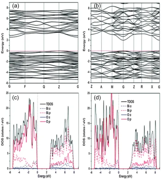
the narrow bandgap. Figure 1.3 shows the calculated band structure and electronic density of α-Bi2O3 and
β-Bi2O3.The conduction band of the Bi2O3 is dominantly constructed by the Bi 6p orbital. The shallow valence band
maximum is mainly composed of hybridized Bi 6s and O 2p orbitals, which leads to the narrow bandgap into the visible region. Compared with α-Bi2O3, β-Bi2O3 exhibits a more dispersive band structure leading to narrower
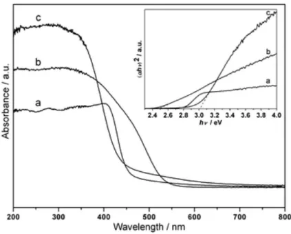
bandgap. Figure 1.4 shows the absorption spectra of α, β and d-Bi2O3. The calculated and measured bandgap of
the α, β, d-Bi2O3 is around 2.80, 2.50, and 3.00 eV, respectively.21
Figure 1.3 Band structure and density of states of (a,c) α-Bi2O3 and (b,d) β-Bi2O3, respectively. Reprinted with
Figure 1.4 UV-vis diffuse reflectance spectra of the Bi2O3 polymorphs: (a) α-Bi2O3, (b) β-Bi2O3, and (c) δ-Bi2O3;
Insert: the corresponding plots of (αhν)2 vs energy (hν). Reprinted with permission from [21]. Copyright 2010
Royal Society of Chemistry.
The synergistic effect of the crystal and electronic structures on the photocatalytic performances of Bi2O3
polymorphs was investigated by decomposing the organic pollutants under the visible light at room temperature.21
Figure 1.5 represents the photodegradation of methyl orange over various phase of bismuth oxide. Among these three phases, the β-Bi2O3 exhibits the best photocatalytic performance, indicating the high absorption ability of
the visible light which is well corresponding to the narrowest bandgap among these three polymorphs. Besides, the tunnel-like structures of β-Bi2O3 efficiently promote the transportation of the photogenerated carriers.
Figure 1.5 Photodegradation of methyl orange with time over different photocatalysts under visible irradiation. Reprinted with permission from [21]. Copyright 2010 Royal Society of Chemistry.
β-Bi2O3 can also be applied as the visible light absorption photocatlysts for water splitting. In order to
split the water, the semiconductors photocatalysts must fulfill two requirements: 1) suitable bandgap which can absorb the visible light, 2) the conduction band minimum is more negative than the redox potential of H+/H2 (0 V
vs VNormal Hydrogen Electrode (NHE)), and valence band maximum is more positive than the redox potential of O2/H2O
(+1.23 V vs VNHE). Because of the narrow bandgap and suitable position of conduction band (negative than 0 V
vs NHE) and valence band (positive than 1.23 V vs VNHE), β-Bi2O3 is a kind of promising photocatalyst for the
application of water splitting. β-Bi2O3 film photoanode with nanoporous surface shows the better
photoelectrochemical activity at the a bias of 0.197 V vs VNHE than that of film photoanode with dense surface.22
Because of the nanoporous surface, the incident light is reflected between the crystal grains and the electrolyte on the surface rather than pass through the film directly, which significantly enhanced the photon absorption ability. Besides, too thick thin films will cause severe electron-hole recombination due to the too long carrier transfer distance. M. Kim demonstrated the fabrication of films of highly textured β-Bi2O3 pillars, which exhibits high
stability over 12000 s and photo current density of 0.97 mA·cm2 at 0.5 V vs. Ag/AgCl.23 The pillar morphology
of β-Bi2O3 delivers a short charge-transfer pathway leading to the enhanced photoelectrochemistry performance.
b) Oxygen ionic conductivity
The 6s2 lone pairs of the Bi3+ cation generally leads to a highly distorted anion with the cation’s located
with one vertex vacant. The d-Bi2O3 possesses a disordered cubic fluorite structure with higher concentration of
intrinsic oxygen vacancy, exhibiting the fast oxygen ionic conductivity.11 The α-, β-, γ-Bi2O3 are all rather poor
ionic conductors because of the highly ordered crystal structure.25
During the past several decades, there are few reports on the oxygen ionic conductivity of β-Bi2O3.The
ionic conductivities of the α, β, γ, δ-phases were systematically measured by the thermal conversion of Bi2O3.24
Typical results obtained during repeated heating and cooling runs are presented in Figure 1.6. With the increase of temperature higher than 500 ºC, the ionic conductivity increases gradually. At around 730 ºC, the ionic conductivity increased sharply because of the phase transformation from alpha to delta phase. During the cooling process, a hysteresis was observed at around 650 ºC, indicating the phase transition to β and γ phases. However, the ionic conductivity of β phases was between 10−4 and 10−3 S/cm at the temperature range from 500 to 650 ºC,
which is much worse than that of d-Bi2O3, similar to that of yttria-stabilized zirconia.
Figure 1.6 Ionic conductivity of various phases of Bi2O3 as a function of temperature. Reprinted with permission
Recently, the ionic conductivity of β-Bi2O3 polycrystalline thin films was measured between room
temperature and 400 ºC ( Figure 1.7 ).25 The ionic conductivity was around 10−5 W•cm–1 at the temperature of 400
ºC. The ionic conductivity during the heating and cooling process are nearly same indicating β-Bi2O3 is stable
below 400 ºC.
Figure 1.7 Ionic conductivity of β-Bi2O3 thin film as a function of temperature. Reprinted with permission from
[25]. Copyright 2016 Springer nature.
1.2.4 Synthetic methods
Table 1.2 summarizes the previous reports on synthesis of β-Bi2O3. Unlike d-Bi2O3 with varieties of
reports on synthesis, the number of reports on metastable β-Bi2O3 is limited. As described above, general thermal
treatment tends to result in the formation of stable α-Bi2O3 or multiple phases. However, some combinations of
appropriate methods, precursors, and conditions enabled to stabilize β-Bi2O3. This section reviews the methods to
Table 1.2 Previous synthetic researches on β-Bi2O3
Sample form Method Temperature Bi precursor Ref
Nanowires
Metal Vapor Transport Deposition
800 °C Bismuth metal 26
Metal-organic chemical vapor deposition (MOCVD)
400–500 °C Bi(CH3)3 27
Nanocrystals/po wders
Hydrolysis and post-annealing around 400 °C Bi(NO3)3·5H2Oor bismuth oxide clusters 28– 33 Thin films
Electrochemical oxidization 200–600 °C Bismuth metal 34
Solid-phase crystallization 300 °C
Bi (001) film and BiOx
amorphous film
35 Aerosol-assisted CVD 300–450 °C Bismuth carbamate 36
Photochemical synthesis 250 °C Bismuth (III)-N-methyldiethanola-mine complex 25 Spray pyrolysis
450 °C Bismuth (III) acetate 37 370 °C
Bi38O45(OMc)24(DMSO)9
·2DMSO·7H2O
38 Spin-coating 300–450 °C Bi(NO3)3·5H2O 39
Sputtering 250 °C Bismuth metal 22
MOCVD 450 °C Bi(OtBu)3 40
Microwave-assisted chemical synthesis
a) Nanocrystals and nanowires
β-Bi2O3 nanowires have been synthesized with oxidative metal vapor transport deposition and
metal-organic chemical vapor deposition.26,27 In the former method, nano-scale droplets of bismuth were oxidized by O2
at moderate temperatures of 250–350 °C (Figure 1.8), resulting in ultrathin β-Bi2O3 nanowires with a diameter of
7 nm and a length of several micrometers,27 which can be controlled by the collection zone temperature. The
spatial-temporal separation of Bi evaporation, vapor transport, droplet formation, and oxidative nucleation and growth achieved the stabilization of the β-Bi2O3 nanowires. For the metal-organic chemical vapor deposition, the
O2 and trimethylbismuth (boiling point = 108.8 °C) were used as the oxygen and bismuth precursors, respectively.
One-dimensional nanowires with a diameter of 30 – 90 nm was obtained at 400 °C, while cluster-like or film-like structures were obtained between 450 and 500 °C.26
Figure 1.8 Schematic diagram showing the growth mechanism of β-Bi2O3 nanowires. Reprinted with permission
from [27]. Copyright 2006 Wiley.
Synthesis of β-Bi2O3 nanocrystals have been achieved by several solution processes from various kinds
of precursors, such as bismuth nitrates, bismuth oxalate, and bismuth subcarbonate.21,28–33 Generally, the
metal-organic precursors, with a similar local coordination structure to that of β-Bi2O3, decompose into β-Bi2O3 by
thermal annealing at around 400 °C.
Flower-like β-Bi2O3 microspheres were prepared by the hydrothermal process and subsequent
calcination.31 The intermediates precursor was synthesized from Bi(NO3)3·5H2O, which has a similar XRD pattern
to that of β-Bi2O3 indicating the similar crystal structure. H. Cheng, et al synthesized the β-Bi2O3 by annealing the
Michael Mehring’s group synthesized the nanoscale β-Bi2O3 using a simple hydrolysis/annealing protocol.
Four kinds of bismuth oxido clusters, [Bi6O4(OH)4](NO3)6·H2O, [Bi22O26(OSiMe2tBu)14],
[Bi38O45(NO3)20(DMSO)28](NO3)4·4DMSO and [Bi38O45(OMc)24 (DMSO)9]·2DMSO·7H2O (OMc = O2CC3H5),
were regarded as the ideal precursors. Because all these clusters composed of different numbers of edge-sharing [Bi6O8−x]2(1+x)+ motifs (Figure 1.9).29,32,33 Extension of this structural motif to an infinite network based on
edge-sharing [Bi6O8−x]2(1+x)+ units results in a near face-centered cubic packing of the bismuth atoms similar to the
structures of β- and δ-Bi2O3.
Figure 1.9 Structural relationship between bismuth oxide clusters and β- and δ-Bi2O3. Inset: hydrolysis concept
to obtain bismuth oxide polymorphs starting from different bismuth oxide clusters. Reprinted with permission from [33]. Copyright 2013 Royal Society of Chemistry.
Low temperature hydrothermal process has also been applied for the synthesize of metastable β-Bi2O3
microcrystals under the assist of BiOBr.30 Bi(NO3)3 solution (with 0.02 mol/L of HNO3) reacted with
cetyltrimethylammonium bromide (CTAB) to form the BiOBr. By adding the NaOH solution, BiOBr reacted with OH− to form β-Bi
b) Thin films
All the β-Bi2O3 thin films reported so far were polycrystalline and their surface morphology was highly
dependent on the methods, precursors, and conditions. The synthesis methods can be classified into three types: 1) solid phase conversion, 2) chemical vapor deposition, and 3) solution-process deposition.
One of the most frequently used methods to deposit oxide thin films is physical vapor depositions such as molecular beam epitaxy, pulsed laser deposition and sputtering. In these methods, the precursors are vaporized into atomic and/or ionic species by applying high energy under high vacuum, and are subsequently deposited on heated substrates. Generally, high temperature is necessary to crystalize oxides, which is not very suitable for volatile bismuth. Thus, these techniques were used to deposit precursor thin films of metal bismuth and/or amorphous BiOx at low temperature and converted into β-Bi2O3 in the previous researches.22,35 While nanoporous
thin films were synthesized from metal bismuth thin films on fluorine-doped-tin-oxide coated glass substrates,22
(201) oriented thin films were generated from Bi/BiOx bilayer on glass substrates.35
In chemical vapor deposition, a gaseous precursor is transferred onto the surface of heated substrates and converted into thin films via chemical reactions. The quality of the films is highly dependent on the kind of precursor. In the previous report of chemical vapor deposition for β-Bi2O3, bismuth (III) tert-butoxide was used
as the precursor, resulting in crystallites with various diameters from 0.4 to 2 um.40 The uniform β-Bi2O3 thin films
were obtained on the Si (100) and Al2O3 substrates by controlling the flow rate from bismuth subcarbonate.42
Compared to the conventional physical and chemical vapor depositions, solution-based deposition methods have been more frequently applied for the thin film growth of β-Bi2O3. The advantage of the
solution-based deposition is the flexibility in the choice of precursor, and experimental setup which can be tuned according to the chemical properties of the reactant and product. In the case of β-Bi2O3, atmospheric pressure is beneficial
to prevent the evaporation of bismuth, while low temperature is preferable to obtain the metastable phase. Several solution-based approaches have been reported for β-Bi2O3 as follows. Ultrasonic spray coating of tetrahydrofuran
solution of [Bi38O45(O2CC3H5)24(DMSO)9]·2DMSO·7H2O followed by hydrolysis and annealing resulted in thin
films with a block-like structure of α- or β-Bi2O3.38 The phase was controlled by the annealing temperature where
the former and latter were synthesized at 550 and 370 °C, respectively. In another report, solution of bismuth (III) N-methyldiethanolamine was spin-coated on the glass or polyimide substrates to form the amorphous thin films, which were UV irradiated in the O2 atmosphere at 250 °C to crystalize into β-Bi2O3.25 Room temperature
deposition by electrochemical method from bismuth metal electrode was also reported (Figure 1.10).43
Anodization reaction through citric acid or NaOH aqueous solution resulted in formation of β-Bi2O3 thin films on
platinum or graphite rod, where subsequent annealing improved the film crystallinity. In the electrochemical deposition, the substrates are limited to conducting materials.
Figure 1.10 Schematic diagram of lateral anodization cell setup. Reprinted with permission from [43]. Copyright 2016 Elsevier.
1.3 Bismuth oxyhalides BiOX (X = Cl, Br, and I)
1.3.1 Crystal structures
Bismuth oxyhalide BiOX (X = Cl, Br and I) possess a matlockite-type structure with tetragonal P4/nmm space group symmetry (Figure 1.11).44 The layered structure consists of [Bi
2O2] layers sandwiched by double
halogen layers stacking with nonbonding van der Waals interactions along the c-axis.44 The highly covalent
chemical bondings between a bimuth center and the surrounding four oxygen and four halogen ions form an asymmetric decahedral local geometry, giving rise to highly anisotropic structural, electrical, optical, and mechanical properties as mentioned below.
Figure 1.11 Crystal structure of the BiOX (X = Cl, Br, and I).
1.3.2 Electronic structure
There have been several reports on theoretical calculation for electronic band structures of BiOX series including BiOF.45–47 Although details are different among the reports, because of the significant influence of
spin-orbit coupling and relativistic effects derived from the large mass of bismuth and heavy halogens and the covalent nature of bismuth, some similar trends can be seen.
Figure 1.12 shows band diagrams obtained by density functional theory calculation incorporating electron-electron interaction, relativistic effect, spin-orbit coupling and dispersion interaction.46 Indirect bandgaps
were predicted for all the BiOX and the bandgap energy decreased as group 17 is descended. As seen in the density of state profiles (Figure 1.13), the conduction band minimum was dominated by Bi 6p state for all the BiOX. On the other hand, the valence band top was dominated by oxygen 2p state in BiOF, while the contribution of halogen np state increased on moving down group 17, resulting in the band gap narrowing.
Figure 1.12 Scalar relativistic (dashed lines) and fully relativistic (black lines) electronic band structures of the BiOX series with the hybrid HSE06 functional. The highest occupied state (including spin–orbit coupling) is set to 0 eV. Reprinted with permission from [46]. Copyright 2016 American Chemical Society.
The electrical mobility was highly dependent on the halogen composition and crystallographic direction. As for hole effective mass, BiOCl and BiOBr (0.8 me and 0.7 me) possessed much smaller mass compared with BiOF and BiOI (12.5 me and 1.9 me, where me is free electron mass) along the in-plane Z → R ([010]) direction.
On the other hand, electron effective mass of BiOF, BiOCl, and BiOBr was much smaller (0.5 me, 0.3 me, and 0.3
me, respectively) to the out-of-plane Z → Γ ([001]) direction than to the in-plane Z → R ([010]) direction. BiOI
Figure 1.13 Fully relativistic electronic density of states, including projections onto ion-centered atomic orbitals. The highest occupied state is set to 0 eV. Reprinted with permission from [46]. Copyright 2016 American Chemical Society.
1.3.3 Physical properties
a) Optical absorption and photocatalysis
As predicted by the first principle calculations, BiOX show different bandgaps depending on the halogen composition. Figure 1.14 shows absorption spectra measured for BiOX thin films.48 Indirect bandgaps of 3.7, 3.6.
2.5 and 2.0 eV were measured for BiOF, BiOCl, BIOBr and BiOI, respectively. The decreasing trend down the group 17 was consistent with the theoretical calculations. Such a chemical trend was reproducibly reported although the absolute values possessed deviations probably due to the various morphology and off-stoichiometry.
Figure 1.14 Diffuse reflectance UV-Vis spectroscopy of β-Bi2O3 and BiOX films, where the absorption edges are
marked with dotted lines. The inset shows the change of Eg for the BiOX family films. Reprinted with permission
from [48]. Copyright 2018 Royal Society of Chemistry.
The same thin films were applied for photocatalytic decomposition experiment of indigo carmine dye under illumination of simulated sunlight in alkaline medium (pH ~ 12). Figure 1.15 compares the time-dependent discoloration with the existence of the BiOX thin films and β-Bi2O3 thin film as a reference.48 BiOCl and BiOI
showed the best and worst performances despite the large and small bandgaps, respectively, which was attributed to the difference in surface morphology. Another possible explanation is the significant difference in the electrical carrier mobility predicted by the first-principles calculations.
Figure 1.15 Discoloration efficiency of indigo carmine dye at pH ~ 12 by using β-Bi2O3 and the different BiOX
films under simulated sunlight. Photolysis of the indigo carmine dye solution is also included. Reprinted with permission from [48]. Copyright 2018 Royal Society of Chemistry.
Morphology is another factor to determine the photocatalytic activity. As mentioned later, BiOX show varieties of characteristic morphology such as nanoflake and hollow microsphere.49 In the decomposition reaction
of Rhodamine B dye by the same weight of BiOCl specimens with various morphology under ultraviolet light illumination, the reaction rate increased in the order of common shape < nanoflakes < nanoplates < nest-like structure < hollow sphere. The trend is attributed to the increase of interfacial area because the hierarchical structures such as the nest-like one and hollow sphere can incorporate the dye molecules to their interlayer spaces. Applicability for water splitting was investigated by using BiOX thin films as photoelectrode.50 In
impedance measurements, BiOCl showed a p-type character, while BiOBr and BiOI were n-type. By combining with the optical bandgaps, band positions of BiOX was determined as shown in Figure 1.16, suggesting potential photocathodic activity for BiOCl and photoanodic activity for BiOI and BiOBr. Indeed, the BiOBr thin film exhibit the best O2 evolution activity among the three materials with high photocurrent of 0.3 mA cm−2 at 1.23 V
vs. NHE, where the dominant (001) facets would have promoted the charge separation. Besides, the BiOBr thin film was much more stable against the photochemical reaction than the BiOI thin film.
Figure 1.16 The band positions of the bismuth oxyhalide films compared to the potentials of water splitting at pH 0. Bandgap values of 1.7, 3.2 and 2.6 eV were determined for the BiOI, BiOCl and BiOBr films, respectively. Reprinted with permission from [50]. Copyright 2016 Royal Society of Chemistry.
b) Anodic performance in secondary ion batteries
Anode materials of secondary ion batteries have been widely surveyed in the past few decades to address the increasing demand for energy conservation. Layered materials like BiOX are good candidates for such applications because of the high ionic conductivity and capacity at the interlayer spaces. So far, anodic performance of BiOX for lithium, sodium and potassium ions have been investigated.51–55
BiOI nanosheets were first investigated as an anode for lithium ion battery and reported to have high volumetric capacity of 717 mA h g−1 in the first cycle.51 Later, high capacities of 254 and 230 mA h g−1 at 15
cycle were reported for BiOCl and BiOBr nanosheets, which were higher than that of 137 mA h g−1 for BiOI at
the same cycle.52 Structural and chemical investigations after the charge-discharge process indicated that the
following two-step reactions proceeded with repeating the cycles:
BiOCl + 3Li+ + 3e− → Li3OCl + Bi (1.1)
Bi + 3Li+ +3e− → Li3Bi (1.2)
In the present stage of studies, the low cycle stability due to the collapse of the crystal structure by the reactions above is the largest issue to be solved for the applications.
c) Photoelectric conversion
Development of photovoltaic cells that convert photon energy to electricity is one of the most intensively studied fields in material science to overcome the energy shortage. Within a general photovoltaic cell composed of stacking layers with each function, the core to determine the performance is the photoabsorption layer. Thus, various kinds of solar cells classified by the photoabsorption layers have been developed, such as silicon-based cells, compound-semiconductor-based cells, dye-sensitized cells, and organic cells.56 Recently, solar cells based
on perovskite-type organic-inorganic hybrid materials are attracting much attention because of the high efficiency and easy fabrication process.57 One of the big issues in the perovskite-type organic-inorganic solar cells is the low
stability of the organic part of the compounds. Thus, discovery of inorganic materials with high photoelectric conversion efficiency are highly demanded.
BiOI is a good candidate to replace the perovskite layer because of the suitable bandgap for harvesting the solar energy. Although the research of BiOI solar cell is still limited, application of BiOI to solar cells has been previously investigated.58 Figure 1.17 shows the cross-sectional SEM image of the solar cell composed of
only inorganic materials. The BiOI thin films were stable in the air for at least 197 days, indicting the good chemical stability. Besides, the prepared BiOI solar cell exhibited short-circuit current density of 6.3 mA cm–2
and power conversion efficiency of 1.75% under AM 1.5G illumination. The conversion efficiency was nearly double of those previously reported solar cells based on BiOI or other bismuth halides and chalcogenides, but still much lower than that of perovskite solar cells. A possible limiting factor is the band bending at the interfaces between the BiOI layer and the neighboring hole and electron transport layers observed by photoemission spectroscopy. Another possible factor to suppress the efficiency was the iodine defects formed during the deposition of the adjacent ZnO layer. These results suggested the optimization of interface engineering is required.
Figure 1.17 Cross-sectional SEM image of the all-inorganic BiOI solar cell without Al. Reprinted with permission from [58]. Copyright 2017 Wiley.
Another application of photoelectric conversion by semiconductors is photodetector. Because BiOX has variable bandgaps depending on the halogen composition, they can be used for sensing light from visible to ultraviolet regions. For example, high responsivity was reported for a solar-blind UV photodetector based on 2D BiOCl flakes, where the responsivity was enhanced by increasing working temperature probably because of increase of intrinsic carriers and the improvement of electrode contacts.59 As for visible light region,
BiOI-nanosheet-based photodetector was useful to detect light with wavelength of 473 nm with a highly sensitive photoresponse.60 The photodetector showed responsivity even for ultraviolet light with wavelength of 254 nm by
introducing oxygen vacancy.
1.3.4 Synthetic methods
Because matlockite-type BiOX are stable phases, various synthetic methods have been reported so far. Most frequently used methods are a series of solution processes. Typical precursors are Bi(NO3)3, NaBiO3 and
Bi2O3 as bismuth sources and KX, NaX, organic halides, and ionic liquids as halogen sources.61–63 BiX3 are also
used for the synthesis of BiOX by oxidation reaction. Reflecting the anisotropic crystal structure, BiOX show various kinds of morphologies depending on the synthetic methods. For application purpose, nano- to micro-scale crystals have been intensively studied so far. This section reviews the previous reports on synthesis of BiOX by classifying them with the morphology.
a) One-dimensional (1D) structures
1D structures such as wires and fibers are suitable for catalytic applications because of their large surface area. A typical method to obtain 1D structures is templating methods. Nanoporous anodic aluminum oxides and activated carbon fibers have been reported to be applicable as templates for synthesis of nanowires and microfibers of BiOCl, respectively.64,65 In both cases, BiOCl was synthesized from solutions. Another way to synthesize 1D
structure is electrospining method, where 1D nanofibers were synthesized by applying high electric voltage to precursor solution from a metallic pin.66 BiOCl nanofibers were synthesized from a viscous N,N- dimethyl
formamide solution of BiCl3 with additive of polyacrylonitrile.
b) Two-dimensional (2D) sheets
Chemical vapor transport method has been frequently used to synthesize single crystals of BiOX on substrates such as mica.59,60,67 These crystals typically have sheet-like morphology reflecting the layered crystal
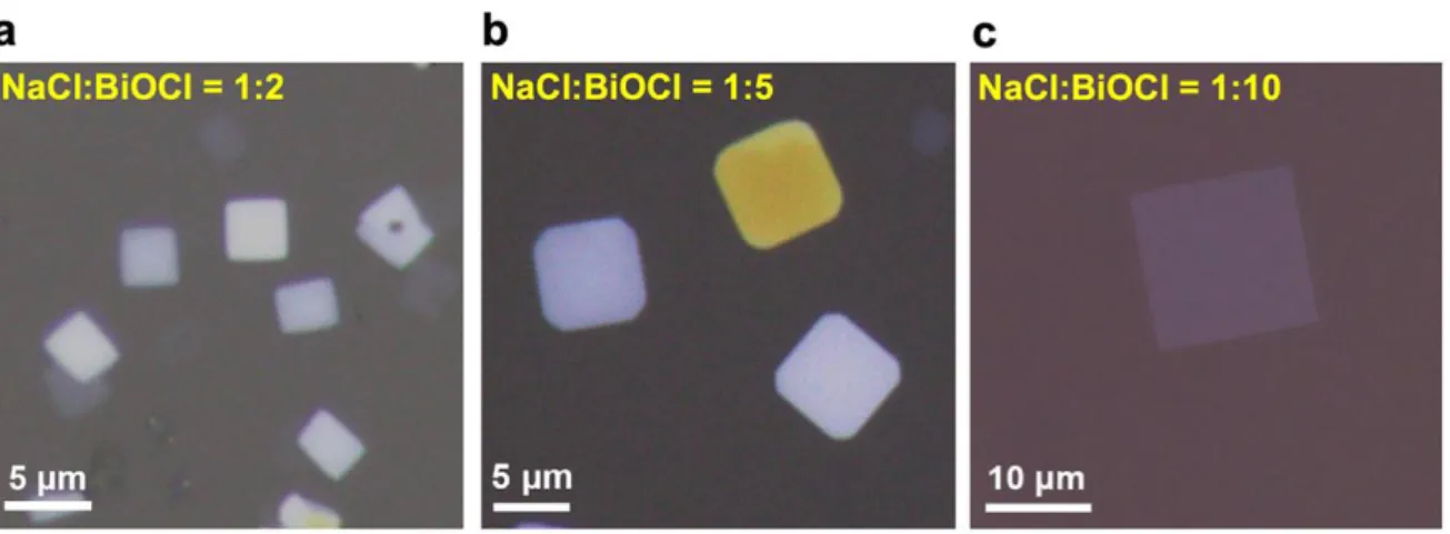
thermally vaporized and transferred onto the surface of substrate placed at lower temperature part. The size of crystals was controlled by the condition and deposition time typically in micro- and nano-scale to lateral and vertical directions, respectively (Figure 1.18). The single crystals with flat surface are useful to construct multilayer devices and measure physical properties such as conductivity.
Figure 1.18 Typical optical images of BiOCl flakes obtained by using different ratios of salt to precursor (mass ratio), showing that the nucleation density of BiOCl flakes is reduced, and their lateral size is increased, with the decrease of the proportion of salt. Reprinted with permission from [59]. Copyright 2020 Wiley.
c) Three-dimensional (3D) hierarchical structures
BiOX show various characteristic morphologies when they are organized in 3D way. In most cases, the 3D microstructures are hierarchically composed of aggregated 2D platelets reflecting the layered crystal structure. Such microcrystals have been frequently synthesized from solution, and the morphology is highly dependent on the experimental condition.
For example, heat treatment on Bi(NO3)3 dissolved in nitric acid solution with addition of sodium halides,
poly(vinylpyrrolidone), and citric acid resulted in formation of spherical microstructure of BiOX.68 The halogen
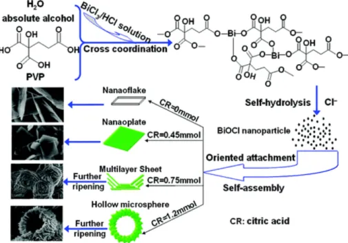
composition was flexibly controlled by the concentration of sodium halides, which is a great advantage of solution processes. The concentration of the additives is one of the key factors to determine the morphology. In solvothermal reactions of BiCl3 dissolved in ethanol and water mixture with the same additives, the morphology
of BiOCl changed from nanoflakes through nanoplates and nest-like structure to hollow sphere by increasing the concentration of citric acid (Figure 1.19).49 This result indicated that citric acid worked not only as a
Figure 1.19 Formation of BiOCl nano-/microstructures under various concentrations of citric acid. Reprinted with permission from [49]. Copyright 2012 American Chemical Society.
Solvent-free mechanical grinding method was also demonstrated recently.62 BiOX hierarchical
flower-like nanostructures were synthesized by mixing and grinding bismuth nitrate pentahydrate with potassium halides via the following chemical reaction (Figure 1.20):
Bi(NO3)3·5H2O + HX → BiOX + KNO3 +HNO3 +H2O
In this reaction, the nitric acid included in the products promoted the further reaction of Bi(NO3)3 and nucleation
of BiOX, resulting in formation of nanoflakes. With increasing the grinding time, the monolayer plate-like flakes assembled into flower-like nanostructures.
d) Thin films
Since the micro- or nano-scale sheets mentionde above are not suitalbe for large area devices such as solar cells, thin films covering the full suraface of substrates are also necessary for applications. Also thin films are useful for measurements of physical properties such as electical conductivity and optical absorption.
Chemical vapor deposition is one of most frequently used technique to synthesize epitaxial thin films of semiconductors. In 1998, Shuisky et al. reported film growth of BiOxIy on MgO (100) substrates by using BiI3
and O2 gas as the precursor and process gas, respectively.69 Figure 1.21 shows the phase diagram of the obtained
thin films. Matlockite-type BiOI was synthesized at only one point among the examined conditions and iodine tended to be run short in most cases. Besides, the BiOI film showed separated growth and did not cover full surface of the substrate, although it was epitaxially grown. There has been no other report on film growth with such vacuum-based technique, probably due to the difficulty in controlling the chemical composition.
Figure 1.21 CVD stability diagram for the BiI3-O2 system. Reprinted with permission from [69]. Copyright 1998
The Electrochemical Society.
Instead, solution-based processes have been reported later. The simplest way is successive ionic layer adsorption and reaction (SILAR) method (Figure 1.22).70 Successive immersing of FTO-coated glass substrates
to the solutions of bismuth and halogen precursors resulted in the formation of BiOX films. The films were composed of aggregated nanosheets vertically grown on the substrates. Immersing to solution is also useful to convert Bi2O3 thin film into BiOX. BiOF, BiOCl, and BiOBr thin films were obtained by immersing precursor
β-Bi2O3 films in HF, HCl, and KBr solutions, respectively, at ambient temperature.48 For bismuth oxyiodide,
conversion was not completed. The thin films were composed of nano-platelets like in the case of the SILAR method.
Figure 1.22 Schematic illustration of the preparation of the BiOX films via the SILAR method. Reprinted with permission from [70]. Copyright 2018 Elsevier.
Spray pyrolysis is another facile solution-based method. In this method, precursor solution is sprayed onto heated substrate and the film is synthesized by the evaporation and chemical reaction of the precursors. Spray pyrolysis of BiOI thin films from ethylene glycol solution of Bi(NO3) and NH4I has been reported so far, where
temperature was an important factor to determine the morphology and composition of the thin films.71 Similarly,
to the immersing method, the films were composed of nanoplatelets.
As a more controlled method, aerosol assisted chemical vapor deposition method was applied for a series of BiOX thin films.50 In this method, N,N-dimethylformamide solution of bismuth halides nebulized with a
piezoelectric device were transferred onto heated FTO-coated glass substrates. The resulting thin films were composed of nanoplatelets with improved flatness and density.
1.4 Overall objective of this study
As mentioned in the previous section, synthesis of thin films is important both for fundamental research and applications. Especially, single crystalline thin films with flat surface are demanded. To this end, epitaxy is widely used for semiconductors and oxides, where the films are grown with a specific crystal orientation aligned
along the crystal structure of single crystal substrates. So far, epitaxial growth of bismuth-based oxide and mixed anion compounds have never been reported. The purpose of this study is development of a facile method to grow high-quality epitaxial thin films of metastable β-Bi2O3 and BiOX.
The main issues in synthesis of these bismuth-based compounds are volatility of the component elements such as bismuth and halogens and the anisotropic crystal structure. To overcome these difficulties, I adopted mist chemical vapor deposition, a solution-based deposition technique performed at atmospheric pressure. Compared with the conventional deposition techniques, mist CVD possesses various advantages such as low environmental load, low cost, simple system configuration, and easy maintenance. Despite a recently developed technique, there are some reports on synthesis of high-quality epitaxial oxide thin films.
This thesis is constructed of 5 chapters. In the present chapter, previous researches on the target compounds are overviewed. In chapter 2, experimental techniques are introduced with an especial focus on the mist CVD method. Chapter 3 explains the results of the study on β-Bi2O3 thin films. Process optimization,
characterization of the films, investigation on the growth mechanism, and improvement of film quality are discussed in detail. In chapter 4, synthesis of a series of BiOX epitaxial thin films is focused. In addition to process optimization and film characterization, composition dependence of the growth manner and tunability of lattice constant by using epitaxial force are discussed. Chapter 5 summarizes the thesis.
Chapter 2
Experimental techniques
2.1 Mist Chemical Vapor Deposition
Mist chemical vapor deposition is a recently developed facial solution-based deposition technique at atmospheric pressure, gaining much attentions as a simple, inexpensive, energy-saving, and non-vacuum process compared with the conventional vapor deposition techniques. So far, the main targets of mist CVD were binary oxide semiconductors with large bandgaps such as ZnO, SnO2, and Ga2O3 (Figure 2.1). Although the thin films’
quality in the previous reports are highly fluctuating, high quality film comparable to that of film grown by the vacuum-based conventional deposition methods is achievable by fine optimization of the synthesis condition.
Figure 2.1 Functional oxide thin films grown with mist CVD.72–86
A general apparatus of mist CVD is composed of a supply unit and a reaction unit as shown in Figure 2.2.87 The supply unit consists of a solution tank equipped with ultrasonic transducers and gas inlets, while the
reaction unit is a heating chamber. In the supply unit, the precursor solution in the tank is nebulized into microscale mist by the ultrasonic transducers. The mist is then transferred to the reaction unit by the carrier gas with a
controlled density by the dilution gas. When the mist reach at the heated substrates placed in the reaction unit, thin films are formed by the thermal decomposition and/or chemical reaction of the precursors.
Figure 2.2 Schematic setup of mist CVD. Reproduced with permission from [87]. Copyright 2014, The Japan Society of Applied Physics.
Although a solution is used as precursor, mist CVD is classified as one of vapor deposition processes because of the characteristic motion of the mist in the reaction unit. As shown in Figure 2.3, the mist droplets transferred in the reaction unit is surrounded by the partially vaporized solvent. The droplets reach at the substrate surface before completion of the solvent evaporation by the fast gas flow. On the surface of the substrate heated at sufficiently higher than the boiling point of the solvent, partial vaporization is promoted at the interface between the droplets and the substrate. Because the solvent vapor suppresses the heat flow from the substrate to the droplets, the droplets keep the liquidous state for a certain time allowing fast and long-distance migration on the substrate surface, which is called Leidenfrost effect.87,88 During the migration of the droplets, exchange of heat and
precursor molecules occurs via the vapor between the droplet and the substrate. Thus, this technique is classified as one of the vapor phase depositions. Until the full vaporization of solvents and byproducts, the droplets keep supplying the reactants to the substrate surface, resulting in gradual and uniform deposition of the product film.
Mainly three types of setups have been developed for mist CVD so far: hot wall type77,89, fine channel
type87,90, and linear source type mist CVD91,92 (Figure 2.4). Appropriate setup is different depending on the
requirement for the films such as crystallinity, thickness, and areal size.
Hot wall type mist CVD is suitable for synthesis of high-quality crystalline films, such as epitaxial thin films. In this setup, tubular furnace is used as the reaction unit, and the substrate is placed on a holder with a certain degree of tilt. Compared to the other types, high temperature is applicable because of the fast mist flow, promoting crystallization efficiently. Also, byproducts are quickly removed by the gas flow and the large temperature gradient between the substrate and the surrounding gas, suppressing the formation of defects. Generally, the deposition area is limited to a few cm2 due to the large temperature gradient.
Fine channel type mist CVD enables the deposition of a large area with high uniformity. The reaction unit of fine channel type mist CVD is composed of a gas mixing part and a fine channel equipped with a heater. The role of the mixing part is reduction of gas pressure to make the gas flow uniform. The flow path in the fine channel part is designed to be longer (typically 100 mm) than the samples to homogenize the temperature of the flowing gas. According to computational simulation, the flowing gas reached at the same temperature as the reactor at the position 15 mm from the inlet of the fine channel if the height of the space is 1 mm. The limited space of the fine channel is also effective in avoiding reevaporation of the films, thus especially suitable for volatile elements.
Linear source type mist CVD provides a high-yield deposition to a further large area. In this setup, the mist is supplied with a curtain-like flow from a movable nozzle scanning between the two edges above the heated substrate, forming homogeneous films in a large area of several 10s cm2 scale. On the other hand, film degradation
is inevitable due to the too large temperature gradient and the open-air construction. Linear source type setup is mainly used in application processes.
Figure 2.4 Schematic of mist CVD apparatuses. Reproduced with permission from [77, 87, 91]. Copyright 2006, 2008, and 2014, The Japan Society of Applied Physics.
In this study, I adopted the hot wall type mist CVD to synthesize epitaxial thin films of the bismuth-based compounds. Figure 2.5 shows a photograph of the equipment. A tubular furnace equpped with a quartz tube of 50 mm in diameter was used as the reaction unit. N,N-DMF was used as solvent and nebulized at 2.4 MHz by a couple of trasducers. The diameter of the mist droplets is between 2 and 3 µm, calculated by the Lang’s formula93:
𝑑 = 0.68 (πT 𝜌𝐹0)
2 3
where T is surface tension, ρ is the liquid density, and F is the exciting sound frequency. 0.68 is an experimental value.
Figure 2.5 Photograph of hot wall type mist CVD system.
2.2 Precursor selection
As a preliminary experiment, I attempted β-Bi2O3 film deposition by using several Bi compounds such
as bismuth nitrate and bismuth citrate as precursors for mist CVD. Among them, only bismuth (III) 2-ethylhexanoate (C24H45BiO6, BiEH, CSID: 2299191) formed thin films. Here I briefly summarize the previous
reports on the decomposition reaction of BiEH.
Figure 2.6 shows the result of thermogravimetry for BiEH in Air, N2, and 10 % H2 diluted with He. In
N2, two step decomposition reactions described as follows were observed at 250 °C and 400 °C, respectively:
2 Bi[OOCCH(C2H5)C4H9]3 (l) 4567 8⎯: 2 BiO[OOCCH(C2H5)C4H9] (s) + 2 O[OCCH(C2H5)C4H9]2 (g) (2.1) 2 BiO[OOCCH(C2H5)C4H9] (s) 4567 8⎯: β-Bi2O3 (s) + O[OOCCH(C2H5)C4H9]2 (g) (2.2)
Here β-Bi2O3 was preferentially formed as products probably because of the similar local coordination state of Bi
Figure 2.6 Thermogravimetric analysis results for (a) bismuth (III) acetate (BiAc) and (b) bismuth (III) 2-ethylhexanoate (BiEH). Heat treatments are under N2 (···) or air (---). The solid line shows the experiment
where the reaction is held at 250 °C for 15 h under 10% H2 in He (—). The labels on the right-hand side represent
the theoretical weight losses for Bi precursors to transform into the different compounds. Reprinted with permission from [94]. Copyright 2000 Royal Society of Chemistry.
2.3 Crystallographic characterization
2.3.1 X-ray diffraction
X-ray diffraction (XRD)95–102 is a most frequently used technique for characterizing crystal structure
because of the characteristics such as 1) non-destructive method without special sample preparation, 2) flexibility in measurement atmosphere and pressure, 3) controllability of the analysis depth by the incident angle, 4) high resolution, and 5) transmittivity of X-ray enabling observation on buried interfaces. For epitaxial thin films, XRD is applicable for identification of crystalline phase and in-plane orientation and evaluation on crystallinity and thickness.
An inorganic solid crystal has a periodic structure in an angstrom order. When X-ray with a wavelength comparable to the periodicity is incident on the crystal, diffraction from the lattice plane occurs to the direction determined by the following Blagg’s law (Figure 2.7),
2d sin θ = nλ (2.3) where d is the lattice plane distance, 2θ is the angle between the incident X-ray and the detector, n is an integer, and λ is the wavelength of X-ray. Lattice constants of the sample can be calculated from the 2θ values of the diffraction peaks by using Blagg’s equation.
Figure 2.7 Schematic image of Blagg’s equation.
Figure 2.8 shows the setup of a four-axis XRD apparatus composed of an X-ray generator, a sample stage on a goniometer, a detector and a monitor. ω denotes the incident angle of X-ray. φ and χ correspond to the rotation angles about out-of-plane and in-plane axes of the sample surface, respectively.
Figure 2.8 Schematic image of the measurement configuration of XRD equipment.
In this study, XRD measurement were performed with a four-axis diffractometer (D8 DISCOVER, Bruker AXS) by using Cu Kα characteristic X-ray (λ = 1.5418 Å). I used 0D (spotty), 1D (linear) and 2D (circular) detectors depending on the purpose. With increasing the detector dimensions, the detection range becomes larger while the resolution becomes lower.
In θ–2θ scan, diffractions from the lattice planes parallel to the surface are measured by varying ω and 2θ under symmetrical setup (namely, ω = θ). This technique is frequently used as survey measurement to determine the crystal structure and phase purity of thin films. I used the 1D detector in θ–2θ scans.
Rocking curves are measured by sweeping ω with fixed 2θ at a diffraction angle. Because they reflect the distribution of the measured planes, the full width at half maximum (FWHM) of rocking curves is used as a measure of crystallinity. 0D detector was used to measure rocking curves in this study.
Reciprocal space mapping (RSM) is a powerful method to determine the crystallographic orientation and lattice constants of epitaxial thin films. By varying ω and 2θ independently from each other, diffraction intensity is mapped in ω–2θ space, which can be converted to reciprocal space. I used the 1D detector instead of sweeping the detector.
On the other hand, intensity mapping in 2θ–χ space is possible by using a 2D detector. In this setup, diffractions from the lattice planes directed out of the surface normal are detectable. Thus, it is useful for measurement on compounds with asymmetric structure like β-Bi2O3.
2.3.2 Raman spectroscopy
Raman spectroscopy103 is sensitive to bonding states in materials, and thus useful to identify crystalline
phase of inorganic compounds. When light with energy of hν0 is irradiated to a sample, a part of the photons is
scattered in elastic and inelastic ways. In the elastic scattering process, also called as Rayleigh scattering process, the energy of the light is conserved while the momentum is changed. From the viewpoint of interaction between the photons and the material, the elastically scattered photons can be considered as emission from the virtual excited vibration mode with higher energy than the ground state by hν0 of a chemical bonding (Figure 2.9). Raman
scattering is the strongest inelastic scattering. In Raman processes, the energy of the vibration mode is changed by ΔE through the scattering. Thus, the energy of the scattered photon is also changed from hν0 to hν0−ΔE. The
scattering process with positive and negative ΔE are called Stokes and Anti-Stokes processes, respectively. Because the value of ΔE is specific for each bonding state, Raman spectra provide the information of local coordination.
In this study, I used a Raman microscope (NRS-5100, JASCO) equipped with a green laser (λ = 532 nm). Because Bi2O3 possesses at least 7 polymorphs with similar Bi–O length, it is hard to distinguish them by XRD.
On the other hand, Raman spectra are highly different depending on the crystalline phase as shown in Figure 2.10. Thus, I applied Raman spectroscopy to confirm the crystalline phase of Bi2O3.
Figure 2.10 Raman spectra of: (1) d-, (2) β-, (3) d -and β-, (4) d -and β-, and (5) α-Bi2O3. Reproduced with
permission from [104]. Copyright 2006 Institute of Physics.
2.3.3 Atomic force microscopy
Atomic force microscopy (AFM)105,106 is an observation technique for surface morphology with a high
height resolution in nanometer scale. A schematic image of AFM is shown in Figure 2.11. AFM uses an atomically sharp probing tip attached at an end of a cantilever. When the tip is close enough to the sample surface, it is subjected to the atomic force following the Lennard-Johns potential. In contact mode AFM, which was used in this study, the tip is placed at a height closer than the minimum of the Lennard-Johns potential, resulting in repulsive force between the tip and sample surface. During the measurement, the tip is swept in horizontal direction and the cantilever is deflected and inflected when the distance between the tip and the sample surface get smaller and larger, respectively. Thus, the height of the sample can be measured by observing the tilt angle of the cantilever with the laser irradiated on the top of it. In actual measurements, the height of the tip is kept at a constant by changing the height of the sample stage with the feedback system, whose signal constructs the 3D image of the surface morphology.
Figure 2.11 Schematic image of the measurement configuration of AFM equipment.
In this study, a commercial AFM system (SPI-4000, Hitachi High Technologies) was used. Tilt correction was applied for the AFM images, and the root-mean-square (RMS) roughness was calculated for 2 × 2 µm2 images.
2.3.4 Scanning electron microscope
Scanning electron microscope (SEM)107–109 is a microscope using electron beam as the probe to observe
morphology of samples. The basic setup is shown in Figure 2.12. In this measurement, the sample is irradiated with finely focused electron beam accelerated by electric field. A field emission gun provides much finer electron beam than previously used thermal emission guns, enabling high spatial resolution measurements. When the primary electron beam reach at the sample surface, the sample emits secondary electrons in addition to reflection electrons, where the intensity of the former is dependent on the sample shape. By scanning the electron beam, one can obtain the image of the sample morphology. Compared to AFM, much wider region from submicro- to mili-meter can be measured while the height resolution is lower.
Figure 2.12 Schematic image of the measurement configuration of SEM equipment.
In this study, sample morphology was observed by a field-emission SEM (S-4800, Hitachi High Technologies and JSM-7800F, JEOL). Because the samples prepared in this study are insulators, I deposited 1–2 nm thick osmium conducting layer on top of the samples by low-vacuum chemical vapor deposition before the measurements.
2.4 Elemental analysis
2.4.1 X-ray photoemission microscopy
X-ray photoemission microscopy (XPS)110,111 is a technique to measure electronic states of the elements
in materials, applicable for all the elements except for H and He. When a sample is irradiated with X-ray with a constant energy of hν, an electron occupying a certain energy level Eb can be excited and emitted out of the sample
if the kinetic energy Ek is positive (Figure 2.13). Ek is given by the following equation.
Ek = hν − Eb – Φ (2.4)
where Φ is the work function of the sample. If measured from the Fermi energy, Eb is given as
Eb = hν – Ek (2.5)
Thus, Eb can be determined by measuring the velocity of the emitted electron, for which hemispherical analyzers
are often used. While the energy of the core electrons is element specific, the energy of the valence electrons is dependent on the chemical state of the element. Accordingly, valence state of component elements in materials can be determined. Because the escape depth of electrons is about 1 nm, depending on Eb, XPS measurements are
generally surface sensitive. Although XPS can be also used for composition analysis, it is semiquantitative because the peak intensity is a function of not only the composition but also other factors such as the apparatus setup and sample morphology.
In this thesis, the chemical states of the constituent elements were investigated with XPS (AXIS-Ultra DLD, Kratos) by using Mg Kα characteristic X-ray (hν = 1254 eV). The peak positions were corrected with the C 1s peak at 284.2 eV.
Figure 2.13 A schematic image of the photoelectric effect and XPS spectrum.
2.4.2 Energy dispersive spectroscopy
The energy dispersive spectroscopy (EDS)112 technique is widely used for qualitative analysis of
elemental composition of the thin films and bulk materials. The EDS technique detects X-ray emitted from the sample to characterize the elemental composition.
To stimulate the emission of characteristic X-rays from a specimen, a beam of X-rays irritated on the sample. The incident beam will excite an electron in an inner shell in the atom, ejecting it from the shell while creating an electron hole where the electron was, emitting the specific wavelengths of X-rays. The number and
X-ray energy was highly depended on the atomic structure of the emitting element, which was used to the determine the elements composition of the sample.
In this study, the chemical composition of the samples was investigated with EDS by using an energy dispersive analyzer equipped with the SEM (SEM; JSM-7800F, JEOL).
2.5 Optical properties
2.5.1 Ultraviolet-visible-near-infrared spectrometer
I measured optical absorption spectra for the epitaxial thin films of the bismuth-based compounds, which is essential for applications such as photocatalysis and photovoltaics, with an Ultraviolet-visible-near-infrared (UV-Vis-NIR) spectrometer (V-770, JASCO). Absorption coefficient α was calculated from transmittance T and reflectance R by using the following equation:
𝛼 = −2= ln2AB@ (2.6) where t is film thickness. The contributions of multiple reflections are ignored in this equation.
Tauc-plot is frequently used to determine the optical bandgap value from the edge structure of the optical spectra. In a Tauc plot, (αhν)n is plotted against photon energy hν, where a liner relationship is expected for the
band tail with the exponent n of 2 and 1/2 for direct and indirect band transitions. Direct and indirect bandgaps can be distinguished by the linearity of the two kinds of plots, and extrapolation of the line yields bandgap energy.
In this study, I quantitively determined the bandgap and optical absorption coefficient of β-Bi2O3 epitaxial
thin films. Figure 2.14 summarizes the reported bandgap values and absorption coefficient of β-Bi2O3.22,23,25,33
The bandgap values ever reported for β-Bi2O3 broadly ranges from 1.74 to 3.4 eV, and it is still under debate
whether β-Bi2O3 is direct or indirect bandgap semiconductor.
Chapter 3
Epitaxial growth of β-Bi
2
O
3
thin
Films and particles
3.1 Experimental method
I successfully achieved the epitaxial growth of β-Bi2O3 thin films and particles on α-Al2O3 (0001) and
yttria-stabilized zirconia (YSZ) (111) single crystal substrates with hot-wall type mist CVD from Bismuth (III) 2-ethylhexanoate (C24H45BiO6, BiEH, CSID: 2299191). The deposition conditions are summarized in Table 3.1.
2-ethylhexanoic acid solution of 25 wt.% of BiEH (Wako) was diluted with N,N-dimethylformamide (DMF, purity: 99.5%; Wako) into solution with Bi concentration of 0.024 mol/L. The precursor solution was formed into mist by 2.4 MHz transducers and was transferred with N2 gas flow onto the substrate placed in the heated quartz tube.
Table 3.1 Synthesize condition of β-Bi2O3
Precursor solution BiEH DMF solution Concentration of precursor 0.024 mol/L
Substrates α-Al2O3 (0001), YSZ (111)
Deposition temperature 300 – 600 °C
Deposition time 30 min
Carrier gas N2, 3 L/min
Dilution gas N2, 0.5 L/min
![Figure 1.2 Thermal stability of various polymorphic of Bi 2 O 3 . Reprinted with permission from [20]](https://thumb-ap.123doks.com/thumbv2/123deta/5889138.1047736/12.892.239.663.438.718/figure-thermal-stability-various-polymorphic-bi-reprinted-permission.webp)


![Figure 1.7 Ionic conductivity of β-Bi 2 O 3 thin film as a function of temperature. Reprinted with permission from [25]](https://thumb-ap.123doks.com/thumbv2/123deta/5889138.1047736/17.892.204.692.271.639/figure-ionic-conductivity-film-function-temperature-reprinted-permission.webp)
![Figure 1.10 Schematic diagram of lateral anodization cell setup. Reprinted with permission from [43]](https://thumb-ap.123doks.com/thumbv2/123deta/5889138.1047736/22.892.201.699.279.532/figure-schematic-diagram-lateral-anodization-setup-reprinted-permission.webp)