愛知工業大学研究報告 第 48 号 平成 25 年
HEM 構造を用いた半導体量子ドットレーザの単一モード発振
Single mode laser operation of semiconductor quantum dot using HEM structure.
五島 敬史郎✝,津田 紀生✝, 山田 諄✝, 小森和弘✝ ✝, 天野 健✝ ✝
Keisiro Gosima, Norio Tsuda, Jun Yamada, Kazuhiro Komori, Takeru Amano Abstract:We propose a quantum dot (QD) laser with the half-etching mesa distributed feedback (HEM-DFB) structure, fabricated by single-step dry etching. The HEM-DFB structure provides several advantages, such as a low scattering loss, wavelength stability and so on. In this study, we achieved wavelength stability control of two mode emission peaks generated by HEM-DFB structure using improved Cl2 dry etching. Also, we demonstrated low threshold current of 23 mA and higher thermal stability of 0.077 nm/K at a 1.3-m emission by the improved HEM-DFB structure
1.Introduction
Quantum dots (QDs) have attracted more attention than other quantum structures as regards applications to optical devices such as laser diodes because of the intrinsic properties of the self-assembled semiconductor quantum dot, which is three-dimensionally confined and has an atomic-like density of states(1-4). For example, a QD laser should have a lower threshold current density and higher thermal stability. However, there are certain problems in that a QD laser is insufficient as regards modal gain, operation mode control, and wavelength stability. In our previous work, we achieved a 1.3-m high density and high uniformity QD used by our proposed gradient-composition (GC) SRL and an As2 source (5), which density and FWHM is 1 x 1011 cm2 and 22 meV, respectively. We also realized a high modal gain with an 8 cm�1/QD layer at 1.3 m QD laser through the use of our QDs (6.7).
† 愛知工業大学 工学部 電気工学科(豊田市)
†† 産業技術総合研究所・光技術研究部門(つくば市)
On the other hand, high wavelength stability and small signal operation with high-speed modulation are important, for example, for fiber optical communication system applications. Distributed feedback (DFB) laser structure rather than Fabry-Perot structure are essential for stabilizing the emission wavelength of the laser. However, it is difficult for a laser based on GaAs to realize a DFB structure with a grating embedded inside the semiconductor using conventional material regrowth because of the oxidation of the Al-containing layer. One way to avoid the need for regrowth has already been reported and involves using a vertical grating DFB structure fabricated by deep etching the mesa
(8,9). The advantage of this structure is that it can be
aligned and etched together with the mesa through the active region in a single step. However, several problems remain an optimized design for a QD laser and the large optical scattering loss caused by fabrication fluctuation. We have proposed a half-etching mesa (HEM) DFB laser designed for a QD laser in our previous report. Also, we succeeded a 1.3-m emission with HEM DFB structure by using high-density and high-uniformity
QDs. (10,11)
愛知工業大学研究報告,第 48 号, 平成 25 年,Vol.48,Mar,2013
In this study, we improved the HEM-DFB structure using ICP dry etching with Cl2 source. We achieved the clearly DFB characteristic of two mode emission peaks because we suppressed the fabrication fluctuation of a grating. Also, we demonstrated low threshold current of 23 mA and higher thermal stability of 0.077 nm/K at a 1.3-m emission.
Fig. 1 Schematic structure of HEM DFB laser. The inner width, the outer width and the gating variation are Wi, Wo and 0.5m, respectively.
2.Device design and fabrication
We have proposed the HEM DFB laser structure shown in Fig. 1. The HEM structure provides several advantages, such as a low optical scattering loss, wavelength stability, lower coupling coefficient and gain coupling. This structure is realized by etching the vertical gratings only as far as the center of the active layer. In the theoretical treatment, the design parameters for the inner width, the outer width and the grating variation are Wi, Wo
and 0.5m as shown in fig 1. In addition, the refractive index of the core and cladding are 3.2 (GaAs) and 1.5 (SiO2), and the equivalent refractive index of Wi and Wo are ni and no, respectively. The
index coupling coefficient () for the fundamental TE mode can be estimated using the standard coupled mode theory for HEM DFB structures as follows.
(1)
Where b is the Bragg wavelength. From the
calculation, the coupling coefficient of a HEM with the inner grating width of 2.5 m is expected to be approximately 30 cm-1. InAs QD laser wafers were grown by molecular beam epitaxy (MBE) on n-GaAs substrates with an As2 source generated by a valved cracker cell. The laser structure comprises 1.5-m upper and lower AlGaAs cladding layers and a 400-nm GaAs/InAs active region. Nine layers of high-density InAs QDs were confined at the center of the active region [5].
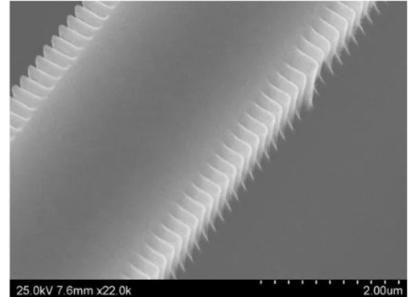
Fig. 2 Scanning electron microscope image of HEM DFB structure.
The DFB fabrication process is as follows (12). First, a first order grating pattern is then drawn by electron beam lithography. The metal mask pattern is formed by using Ti and Ni. Next, the structure is etched to the center of the active region with inductive coupled plasma (ICP). In previous work, we used the dry etching process with BCl3/Ar chemicals. This etching process provides correct etching depth because of a slow etching speed. However, there are remaining issues of an optical scattering loss generated by fluctuation of side grating and the threshold current increased due to
b i o n n 2( ) Vertical grating Active region AlGaAs clad Wi Wo 0.5m Vertical grating Active region AlGaAs clad Vertical grating Active region AlGaAs clad Wi Wo 0.5m 192
HEM 構造を用いた半導体量子ドットレーザの単一モード発振
trapezoidal-shaped.(10,11) Therefore, we improved the dry etching process by using Cl2/Ar chemicals. The mesa structure by using this dry etching is improved to rectangular-shaped, and the fabrication fluctuation of the side grating is suppressed. The etched surface was deposited with SiO2. An n-side and p-side contacts were deposited followed by metallization. Both facets of the samples are cleaved without AR coating. An SEM image of the fabricated HEM DFB structure is shown in Fig. 2, which includes an image of the vertical grating before the SiO2 coating was deposited.
3.Results and Discussion
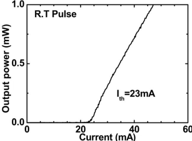
The HEM DFB laser has a 2-mm cavity and a cleaved facet. Figure 3 shows the light-current characteristics at room temperature under pulsed conditions with 1.0-s pulses, and a 0.1% duty cycle. The threshold current, slope efficiency and threshold current density are 23 mA, 0.04 W/A and 383 A/cm2 respectively. The threshold current reduce to 23 mA from 35mA, and the slope efficiency increase to 0.04 W/A from 0.022 W/A. The spectrum under CW operation is shown in Fig. 5. We observed wavelength stability control of the clearly two modes emission peaks (-1 mode: 1.30702 m and +1 mode: 1.30748 m) because the DFB laser does not have a /4-shifted structure. This result shows that the optical scattering loss caused by the fabrication fluctuation of grating is sufficiently suppress and the clearly DFB characteristic is achieved. Addition, the wavelength difference between those two peaks (= 0.465 nm) corresponds to the stop band. The coupling coefficient was assigned as 25 cm1, which is good agreement with the calculation result of 30 cm-1. From these results, we formed a correct HEM-DFB structure using dry etching with Cl2 source Figure 4 shows the emission wavelength as a function of the operating temperature. The emission wavelength changes only 0.077 nm/K in accordance
with the temperature coefficient of the refractive index, which is about a factor of five lower than that of the material gain shift. This thermal stability is reasonable value for the conventional DFB structure.
Fig. 3 I-L characteristic of HEM DFB laser at room temperature under pulsed operation.
Fig. 4 Emission spectrum of HEM DFB laser under 1.2 Ith CW operation.
Fig. 5 Temperature dependence of emission wavelength.
0 20 40 60 0.0 0.5 1.0 R.T Pulse Ith=23mA O ut pu t p ow er (m W ) Current (mA) 1305 1306 1307 1308 1309 -85 -80 -75 -70 -65 -60 -55 -50 I = 1.2Ith =0.47nm Output power (dB m ) Wavelength (nm) 15 20 25 30 1306.2 1306.4 1306.6 1306.8 1307.0 1307.2 1307.4 1307.6 d/dt = 0.077nm/K Wa velengt h ( nm ) Temperature (。 C) 193
愛知工業大学研究報告,第 48 号, 平成 25 年,Vol.48,Mar,2013
4.Conclusion
In summary, we improved the shape of mesa structure and the suppressed the grating fluctuation of the HEM-DFB structure using ICP dry etching with Cl2 source. We observed the clearly DFB characteristic of two mode emission peaks. This shows that the optical scattering loss caused by the fabrication fluctuation of grating is sufficiently suppressed and the clearly DFB characteristic is achieved. Also, we demonstrated low threshold current of 23 mA and higher thermal stability of 0.077 nm/K at a 1.3m emission. At the future work, we fabricate a HEM DFB laser with a /4-shifted structure and AR coating; we can realize single-mode operation and a high SMSR with a 1.3-m emission.
References:
1) Y. Arakawa and H. Sasaki, Appl. Phys. Lett. 40 (1982) 939.
2) M. Asada, Y. Miyamoto, and Y. Suematsu, IEEE J. Quantum Electron. QE-22, (1986) 1915. 3) D. L. Huffaker, G. Park, Z. Zou, O. B. Shchekin,
and D. G. Deppe, Appl. Phys. Lett. 73, (1998) 2564.
4) P. M. Varangis, H. Li, T. C. Newnell, A. Stintz, B. Funchs, K. J. Melloy, and L. F. Lester, Electron. Lett. 36, (2000) 1544.
5) T. Amano, T. Sugaya and K. Komori, Jpn. J. Appl. Phys, 44, (2005) L432.
6) T. Amano, T. Sugaya and K. Komori, Photon. Tech. Lett, 18, (2006) 619.
7) T. Amano, S. Aoki, T. Sugaya and K. Komori, J. Sel. Topics Quantum Electron., 13, (2006) 1237. 8) H. C. Kim, J. Wiedmann, K. Matsui, S. Tamura and S. Arai, Jpn. J. Appl. Phys. 40, (2001) L1107. 9) J. Wiedmann, H. C. Kim, K. Ebihara, B. Chen, M. Ohta, S. Tamura, J. I. Shim and S. Arai, Jpn. J. Appl. Phys. 40 (2001) 6845.
10) K. Goshima, T. Amano, K, Komori, and T. Sugaya, Jpn. J. Appl. Phys. Submitted.
11) T. Amano, K. Goshima, K, Komori, and T. Sugaya, The 21th IEEE International Semiconductor Laser Conference (ISLC 2008), P19.
12) R. Akimoto, C. Guanway, K. Akita, H, Hazama, H. Ishikawa, The Ninth International Conference on Intersubband Transitions in Quantum Wells (ITQW07), T43.
(受理 平成 25 年 3 月 19 日) 194