A Grounded lnductance Using an
Operational AInphfier Pole
and lts Apphcation to Filters
by
Masaru lsHDA*,Hiromu TAFUJI*・
,Yutaka FuKUI*
and Kelsuke EBIsuTANIキ
(Received June ll)1982)
This paper proposes a new sirnulation circuit of a grounded inductance using an operational amplifier pole. The value of silnulated inductance can be varied by a resistance ratio and a gain bandwidth product of the operational amphfier. The proposed structure wor'【s wel over a wide frequency range and has low sensitivity to active and passive elements Theoretical and experinaental results indicate that the realzed circuit is stable overthc wide frequency range and can be used effectively for
a low‐Q actiVe network The practical examples in a highpass ladder filters are also
given together with experilnental verifications
1.Introduction
Recently,operational amplifiers(Op amps)are widely used as inductorless filters,
oscilators,inductor and capacitor sIIlulations in addition to use as active elements.However, a practical op amp dosenot generally ideal becauseofcharacteristicsof frequency― dependent
gain and finite input and output impedanc鶴 .As the result,the use of op amp is lilnited by their fとlite gain bandwidth product.Therefore,many authers have exploited op amp pole in desig ng active R filter,1) 3)inductance and capacitance simulations4)-6)etC.In the previous paper,71 we also prOposed a new integrator using this technique.The utilization Of the op amp pole g es the reliable high freqttency performance,and eliminates the external capacitances fronl the circuit,Therefore,it is suitable for monOnthic lc implementation.
In this paper,we proposed a new grounded inductance simulation circuit which is composed of t、vo op amps and only resistances without req ring any external capacitances.Since the value of sIIlaulated inductance depends prirnarily on resistance ratios,the proposed circuit is suitable for IC implementation.Froni the sensitivity analysis,、 ve proved that the circuit has lo、v sensitivities to all the network parameters.It is shown that the cofigulation can be used
・ Department of Electrical Engineerilag 41 PreSent Address I FurunO Electric CO,,Ltd.
Reports of the Faculty of Engineeimg,Tottori University,Vol.13 41
for active network reaHzing low‐ o and the experirnental results agree、 ven with the analytic
results,
The network analysis based on the single‐ pole rolloff model of op amp, and stability
analysis are also given Then,the highpass filters are designed using the proposed circuit,The experirnental results sho、v that these filters operate successfully as the conventional ones.
2.Theoretical analysis
The new circuit for inductance sirnulation is shown in Fig.1.Asstlming the sigle‐ pole roHoff characteristic for the two op amps,the gain is
4XO―
伴者三―
器舒
,‐
2、vhere z4。ぁω´rand G[',are the opela loop gain,the 3 dB frequencies and the gain bandwidth product of op amps, respectively,and subscriptsゲ are related to op alnp l and op arnp 2. Assuming a typical case l S I≫ ω,ど,the open loop gain 4」 (S)is given by
れ
0-争
… … … …… …図 In Fig, 1,the input impedance Zど ″(s)at the input ternlinals l-1′ is obtained asみ
XO=
24 Fa十,5父分 Ⅲ 十 とι2α5 鳥 Rズ '5+鳥)]+,sR′ [(1+だ1),4+£ ■′]where
,1=鳥Rr―R2亀 α2=寅I R2+■2■′十買1■′ α9=資1+R′ α4=22+Rア α5=R3+R4
and it is to
Eq.(3),we have
・… … … …・・(5)
C/1=鳥 み
+島
鳥 十R4鳥
+R2R4
碗=口亀十買D島
鳥t/3=2Rl鳥 舟 十鳥 鳥 鳥 十Rl鳥鳥 十買l R4み
assumed that 41(s)=42(S)=4(s).Substituting Eq.(2)
z湘 =
事where
Masaru ISHIDA and Hiromu TAFUJI and Yutaka FUKUI and
Grounded lnductance Using an Operational Amphfier Pole and
Keisuke EBISUTANI:A
Its ApplcatiOn to FiltersFig。 l Circuit for inductance sim』 ation
The circuit is adiusted so that(完
鳥
/R3R/1=l by
鳥 and■ん
Z″(S)reduces toFig.2 Equivalent circuit of Fig.1
1he Suitable choice of resistances R2,R3,
Z,ぇ(s)=
In Eq.(7),it is seen that the circuit of Fig.1
resistance Rs in series with a capacitance
componerits are 奉
+SGβ
資′C/8+GB2島
R3鳥
behaves as an equivalent Cs as sho、 vn in Fig. 2, ・……… … ……… ……・・(7) inductance Ls and a where the sirnulatedLs=鵠
・…… … … …… …… …… ……… ……… …… … … …・・(8)Cs=
Gβ是 鳥 鳥 (R′十Rl)1/1tt t/ R′ C/3GB 1/3+1/1R′十R2Rs=
GBF2■
3をThe quality factor o(ω )of a simulated circuit is given α ω
=
where
…… … … …・(10 ■二十by
・ … … … …・,(11)Reports of the Faculty of Engineeirng,Tottori University,Vol 13
Table l calculated values of sinlulated components and Q_factor
Type RIjR2 (n) R3 (■) R4
(→
Rf(n)
Q(l КHI) Ls(H)R5ω
l .0001 10000 1 出 I H 100 2 12・10 3 2 3 .001 1000 100 k l ‖ l H l∞ К l R 100 100 l K l.3S9 1 489 2.12う 10 4 2。12・ 10‐4 11.6 10.7 4 5 6 10 k 100 К 】 H 】 lt i00k 10 k 10 k l К 100 10o l K 10 K ン.316 13 248 14 1,a .09 ・ 10 1 .09・ 10‐l _09・ 10‐1 2.18 2.lB 2.18 ば ば . 0 21.I ll.7 10_7 7 8 9 10 l 10 К 100 k ' K i H 100 k 10 k l H l k 10 K l k 100 K 100 l K 10 K 100 100 K 59 306 101 '50 111 780 1'2 6,0 1.39,10‐2 1_39。lo‐2 1_39・10 2 〕 39・ 10 2 2.67・10 S 2.6,,10‐6 2 6,, 10 6 2 6,、 10 6 20.S 11.7 108. 10, 11 12 13 14 15 10 x 100 K l k l H 100 10 X l k l∞ k 100 l H 10 K l К 100 k l∞ ! H 10 k 100 K I K l H 100 lSa 060 2Rl.910 ■1.'Sl 266 gsO ヨ 696 5 31 ・ 10 3 531●10 3 5 31・ 10 3 S,31, 10 3 5.31・10 3 9_55・ 10 7 , SS'10 7 9 55,10 ア 9.55・ 10` ' 955'10 7 21 2 13_6 9,.6 128 862. l 10 K l K 100 K 100 l k 10 K 100 100k 10 X 100 k l X l H 100 k 10 K l H l К 43.558 10 165 Sa '03 1 2,フ 1.ヨ9,10‐ 2 1.39,10 2 1.ョ9,lo‐2 1.39・10 2 2.67・ lo 6 2.6ア・ 10 6 2.6アD 10 6 2.67む10…6 28_5 116, 19.7 999 100 10 K l К 100 l∞ l k 10 K 10 K 100k l H i H 100K 10 K 4.933 1.ぞ27 144 1.09 1.09 1 09 ば ぃ o ば 2.18・ 10‐5 2.18・ 10 5 2 18θ10‐5 31.4 125. 10,打. 1000 l К iOo 100 l k 100 k l H l H l∞ K .124 011 1 06 1 06 2.13・,0 ・ 213610‐1 12, 1081_ 10000 .0001 100 〕 H I H 00,4 2_12,10 Tl=(し上資:+5りR′ T2=t/3寅′ Te=(R′+疋1)t/1+t/2 T4=t/2+t/3+(し二十鳥 =′ ―鳥R4)々′Ts=亀
鳥 鳥 …… ……… ……… ……… ……・(121Thus、ve note that in Order t0 0btain a fixed value of inductance it is necessary to keep the condition R3翼チ
=■
2R4(=K4ゼ
Ъ=1).Table l shows the calculated values of Ls,Rs,Cs and O for the variott cases. The quanty factor O(ω)indicates a large value in the region of rttistance ratio猛2=氏4=X,=1・
Masaru ISHIDA and Hiromu TAFUJI and Yutaka FUKUI and Keisuke EBISUTANI:A GrOunded lnductance Uding an Operational Amplifier POle and lts ApplicatiOn to Filters
IS=′(C/1 Rl+硯)│《
GB碗
Gβ 2島 鳥 鳥 ≫ld2[(■′+■1)1/1+t/2]│
GB鳥
鳥 岳 ≫ S(C/3+臥買′十鳥)│Then we can be rewritten Eq.(7)in a simple form
みよ
0=生
幽斧迎笠・為お
…… …… ……… … ……… ……・(131
………・(10
Where K2=鳥
/Rl,氏
4=島
/島 andみ
=鳥
/み
It iS dear that Eq.住 n has the property of an ideal inductance,and the inductance value can be varied by changilag the resistance ratiosIG2,頚亀
4 andち
,the gain bandwidth product GB of op arnp and element value買 ′.The valueof the ideal inductance Ls is expressed as
Ls=型
鴇伴立・
為
……… … …… … …… … ……… …… … ……… ……・(151It should be noted that exact value of resistance is iHllnaterial but their ratio is important.
Calculated values of Ls are shown in Table l,where the values of Rs and cs become zerO
under the conditions Eq.l131.
3.Sensitivity function and stability
The sensitivity is a meastlre of the displacement in some performance characterstics of a network resulting from a displacement in value of one orilnore the element of the network. In this chapter,the sensitivities of the rnagunitude of the driving point impedance Z″ (d),the coefficient fOr the nmerator and denominator polynoHlial of the zη (s)and the quality factor O(ω)with respect to displacement in i亀
,F2,R3,買4,亀
R′and GB are derived.The sensiti ty of a network function N(ω )with respect to the element χ is defined by0 Sμ
の
三
鰐許・
チ
・… … … 。(10We can rewite EQ.(7)as shOWn below i
家 0三 ………。(19
where TI,T2,T3,T4and T5 are the same as Eq.QD.The sensitivity ftlllctiOn Of the driving
point impedanceろ
,(s)with respect to a element χ are given byRe S伊°
=
・ァ … ………… …… ……… … ……。(181h Sttω
=
Ч … … … …⑩whue Re Srt7t(。 and lm Sξ力(S)stand for the real and imaginary part of Sξ=21S),rttpectively,
and
Reports of the Faculty Of Enginecirng,TOttOri Univerdty,Vol. 13 45
In the sensitivity functiOns fOr eaёh element,we substitute each of element for tt and the equatiOns as showla below insert in Eq.120.For example,we deduce the sensitivity function Re
s´
猪
(S'for資Ⅲ
Substitutillg Eq.9D illto Eq.9o,and further inserting the resulting Eq.9oin Eq.10,then wc have he Re SP(S'
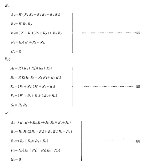
RI; 4。=資′(■ ,十R4)(R?十Fデ) B。=資′
[R′ (2■3+資4)+資,だも
〕
島=(■2■■′)(鳥十買4) FO=R′(■3+々4)十■3(買2+R′)GO=0
XO=40 Ta ω4_GB2(40 TsキBo T4)ωP F。=GBIB。 鳥GB2_(4。T4+BO Ta)ω2]ωχ
l=40T3が
GB子
(TI G。十島FO)の2h=GB[T2Go GB2_(TI FO十
為 どむ)92]ω■=TI T3め
4_GB2(TI T5+T2T4)02
r=Ca[T2集
GB2_(TI T4+T2T3)ω
つ]の £をi 4。=Д′(■3+父4)(R二十R′) BO=R′R3(■二十貴′) ど0=(■ 3+■4)(資′十只二十Rチ) FO=Fチ(■3+資4)十資9(R′+'1+R′
) G。=0
40=R′(■1■ァ+R2資
′十資■■2) β心=R′(2■ 1買′十 '2■ チ十■1■っ) ど。声(資′+RI)(買 2+Rァ)十買2買デ F。=(只rtt Rl)(資2+R′)十只2'′十買′(R′十買1+■2) GO=■2R′ ……・…………Ⅲ…・¨・…・…………・・・…,……'201 ¨●●中中中●¨¨●¨………・…Ⅲ…Ⅲ………Ⅲ¢り …●……,…Ⅲ……Ⅲ…・・t,…・……Ⅲ………Ⅲ…Ⅲ●鬱D Rこ; ……。・・……・Ⅲ………●931弱
肌 言ほ
踏肥監慾ギ報丞謡恐彿露明ぜ評
I訛
士
岳
£
譜乱
監 ♪
R4' 尺′; 4。=軍
(■12′+R,資
′十買IR´) B。こ買ソFi R′ F。=(資′十R■)(資ヮ+資r)十父″尺ァ F。=Rァ(資′十■二十R2) 6。=0
4。=F(■
二十資 “ )(■き十'D
β。こ買<2■1■,十々l資二十■2■9)aO=(R3+■
4)(■′+■ 1+■ ち) F`=(資 ′+ti+資
2)OR3+■
4)CO=■
2 Fa 4。=(資iRテ十F2■ ′十■1■2)(R3+R4) ,i=Rェ F′ (2資 ,十R4)十■2 Fa(Rl+Fデ) DO=(資 デ+F2)(資 こ十資4) F。三資′(R3+R亀)+買よ資2+買′)a=o
……●“…………ⅢⅢ…Ⅲ…Ⅲ……・…………・….……Ⅲ…,941 …………ⅢⅢ…●と'中…●│●│…●●│●¨Ⅲ…・●・●工●……・鬱51 ・・………1,……Ⅲ…Ⅲ…Ⅲ………Ⅲ…●……中●90 f (Hz) l( 10 K 100 KI Figi 4 Calc』attd values of Re&律 tSlⅢpell
R′;
In the same,lanner,he.sensitivity functiOn with respect to GB is as follows
Re S子
女
!(S)随
s亀ド
働
Rl 彰 鳴 監 叶 μl( 10k 100K
ReportS Of the Faculty of Elagineeimg,Tottori University,Vol 13
Re S絡①
=
………・¢ηIm Sそ
τ
lS)= ……Ⅲ………Ⅲ281Wheltwe take typical value lsted up in Table l,each calculated sensit ity factor are shown in Figs,3,4 and 5 to real part and Figs. 6,7 and 8 to imaginary part,respectively.
Next,we deal with the coefficient settitivity of the driving point impedanceる (d),We let N(s)be network function as
Ж
O=
… … … …… ⑩Then,we difine the coefficient sensitivity as fo■
ows:
S?=摯
生
・
哉
SP=プ
う
よ
・
チ
…・―・……・・………,い"¨¨・・…………・
13111
・………・・………・…………・………Ⅲ…………・・・¨…………・・………・・………・ell
where
χ
is any arbituary network element.From Eqs.Q71,00 and 130,the COeficient sensitivityOf Z″(s)for each element can be determined as follows:
SZin(S) Im l・10 1
1.10-2
1・10 5 1・10 41.10-5
_1.10-5
_1.10-4
-1・10 5_1.10-2
-1・10 │SZ,n(S)
f (KHz)
F (KHz)
l K 10 K 100 KFig.5 Calculated values of Re S`'(°
F (Hz) \ \ \ `ヽ
\ `ヽ
\ in type 14
Masaru ISHIDA and
Grounded lnductance
Hiromu TAFUJI and Yutaka FUKUI and Using an Operational Amphfier P。 le and
Keisuke EBISUTANI:A
Its ApplicatiOn to FiltersIm l・ 10 1
1.10-2
1・10 5
1・10 4
1.10-5
_1.10-5
_1.10-4
-1・10 5
_1.10-2
-1・ 10 1SZ:n(S)
SZin(S)
f f Im l・10 11.10-2
1・10 5
1・10 4
1.10-5
_1.10-5
-1・10 4
_1.10-5
_1.10-2
-1・10 110 100
f f(KHz)
(KHz)
10 100
(KHz) (KHz) SII=(資 2+R′)R1/1(■2+R′)R二 十R2資′] S骨 ょ=(■二十 Rデ)R2/1(■二十 Rァ )■2+■1買月 Sl:=R3/1資3+R4)SII=R4/1R3+R4)
Sl与=(R二十 資2)只 ア/[(R二十 R′)R2+Fl々
2] ・…………Ⅲ…Ⅲ…Ⅲ…………・…・………・GD Fig,7 Calculated val■ es oflm Sr'(° in type ll Fig.8 Calculated values Of lm S乙力(。 in type 14Sl,三 1
SttCa=1-■
2 sr:Cを=1-Rl
SttCB=1-RI
S骨4Cβ=1-資
a S吾ザ
β
=1-■
1sr,CD=1
,S:と=0
R3R′R′/T2 F′R′(2R3+R4)/T2 ■4■′資′/T2 買′(2買lR′十■2■′十父1■2)/T2 ■2R9■′/T2笏
Sどず
B=1
………・…・……,……・・・………・ 1331Reports Of the Faculty of Engineei痢 ng, TottOriモ」niversity, V01 13 49 sr】=RI(・2+R′)//8 S骨:=R2(R′
十■
1+R′)//3 S「:R3/1R3+R4)Sri=R4/1R3+R4)
S「み=Rズ
R′十R二十R2)/九 sr,=R′ (R2+Rア)//3 ,S岳
=0
stti CD=Fl(2■3R′十R2R3+R4■
ア)/y4 SI:Ca=寅2(2R3■ア十F2R3+資
4R′)//4 SlとCD=買3(R二十 R′ 十R′)(2R2+寅′)//4sriCa=R4買
′(■1+Rデ十R′)//4 srザ'こR′(R二十資′十R′)(2R3+R4)//4 S,iCβ=R′ (2R3資′十RっFatt R4 R′)//4 SをどC〕=1
sttca2=0 ,sttε ε
2=1
s盈で
,2=1 ,sttCβ 2=0
sttεD2=1 ,stt C'2=0
sttcD2=2
¨・・¨……・¨"・…Ⅲ…………Ⅲ………・・・中¨●e41 ………・¨・―・……・・…Ⅲ………Ⅲ…Ⅲ……・130 Ⅲ…………Ⅲ………・…・¨・……Ⅲ…………,……………・ 1361where
,EI免
難幣 与
与
ill+″
)+資2願
2R3+RD I
…
…
…
…
9りCalculated coefficient sensitivity factors Of the driving point impedanceろ ″(d)by using the
hominal element values in Table l are glven in Table 2-5.Here S´ in not included in the
table,as it is obvious fro■ l Eq.130.The variation in any elements are fotllld to be withn l and
10-4。rder as is ewldent froln these tables.It is clear that the proposed circuit preserlts the low―
Q settit ity to an types and tO aH elemeltts.
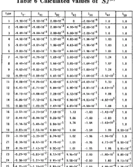
In the same manner as before,the values of sensitivity of O(ω )‐factora)evaluated using Eq.
(lD alld Eq.QO are shOwn in Table 6.
FinaHy, we deal with the stability problem. In general, for an network to be stable, a
numerator and denominator polynominals of the driving point ilnpedance 盪殆″
(s)must be
Htlrwitz polyllominal.From Eq.(7),the driving point impedance Zヵ (d)is written as a ratio of polynoHlinals Rヽ (s)and D。 (d).Thus,it is clear that the polyno■linals N、(d)and DO(d)are given
Masaru ISHIDA and Hiromu TAFUJI and Grounded lnductance Using an Operational
Yutaka FUKUI and Keisuke EBISUTANI:A Arnplifier Pole and lts Application to Filters
as folo、vs I
N。(d)=s2買′(」I RI+助
)+sGB資
′t/s Ⅲ…'¨¨●…●…Ⅲ…………・…………Ⅲ………・………・1381D。(s)=s'[(R′十
Rl)3+協
]+sGB(1/8+凱
資′十買2)+GB2々
2R3買′………99
Table 2 Calculated values of S砕 Table 4 Calculated values of S´
Table 3 Calculated values of SttCβ Table 5 Calculated values of SひCD
“ m m 帥 m 唖 m m Ш 鉤 呻 m m m m
Repolts of the Faculty of Engineeirng,Tottori U versity,Vol.13
In Eqs.981 and 001,SinCe the resistances and the
parameters Gβ of op amp are possitive,zerOs ofハら(S)and DO(s)are in the left‐half S‐plane and origin. Itis Obvious that this proposed
circuit is stable.
Table C Calculated vahes of sPω
〕
'`:0‐
I
4.Experimental results and discussion
The circuit is consisted of six resistances with l percent tolerallce,one potentioコ neter and
two
μ4 747 PC‐ type op amps satisfying tlle condition of the gain bandwidth products G島=
G五ち
=Ga
「Γhe gain bandwidth product of the op amp for a power supply voltage of EL 15 7 is Gβ=2π l.5・ 106筋″/seC.The expernient was carried out mainly using the component
values in table l.The values of sirnulated inductance L and Q― factOr were rneasured by using paranel resonance l■ethod and are given byL=1/2π/。
2c
………109=/。
/(/2 /1)
……… “〕 where/。 is a resOnance frequellcy,andtt and/2“ </2)are the frequencies at cut‐ off frequency.
In Fig. 9, the measured values of the sirnulated inductance are compared with the
theoretical cuビve for four cases,such as L==1.39o10 2H,8.7・ 10 3と I,5.31・ 10 311 and l.48・ 10-311.As is obviott froln this figure,the experinaentat results agree、 ven with the theoretical
ones.
Fig. 10 is an example of a O― factor against frequency taking the resistance ratio頚
色
2 aS a parameten lt shows ho O varies with frequency depending upon the resistance ratio工色
2・Four typical resistance ratios of X12 are Chosen in Fig.10,such as X12=0・ 5(=10 kΩ//20 kΩ),
0.8(=10 kΩ
/12.5kΩ
),1,0(=10 kΩ/10 kΩ),10.0(=100 kΩ/1okΩ
)and 100(=100 kΩ/1kΩ
).For the measurements of O―
factor versus frequency, the resonance frequencies werechanged by adiusting the external standard capacitance.In order to obtain o‐ factor Of over 30,the resistance ratio X12 muSt be chosen within l≦ K2・ Furtherinore,it is difficult for
Masaru ISHIDA and Hiromu TAFUJI and Yutaka FUKUI and Keisuke EBISUTANI:A Grounded lnductance Using an Operational Amplifier POle and lts ApplicatiOn tO FJters
f (KHZ) Fig,9 Theoretic』 and experimental values of
sil■■hted inductance
I i type lo 工 :Rl・ R2・20K■ ,R3・ 2 Kn R4=10 KrL ,Rf=100(■ Ⅲ i type ll 正:町 =R3・ R4・ 10 Kn R2・Rf=100 KrL
ng。
1l Experimenta1 0‐ factor versus
frequency for the various values of R I
and■2 ¬←_ : Rl・ R2・ lK 羽 ― : =2K ゃ 一 : =10K ―e : =100K K34 = Kf2 ・ 1
Fig,10 Experimenta1 0‐
factor verSusfrequency hy varing the resistance
ratio K12 - : 0.5(二 10 Kn/20 Kn ) 十 : 08(・ 10 Kn/12 5 К
n)
― : 1・。(=100 Kr1/10o Kn) コ ー : 10(=100 Kr1/10 KrL) … : 100(=100 Kn/1 Kn)Fig。
12 Experimenta1 0_factor verszs
frequency by varing the resistance
ratios Fa4 and rf2
B : K34 ・ 5,0 , Kf2 ・ 0 2 引 葬 : =2.0 , =o.5 → : =10 , ・ 1・0 - : =0・ 1 , ・ ]00 L(m‖) RI・ 10 Kn ― t theOretical O : eXperimental
Next,an example of a o‐ factor variation、vith frequency are plotted in Fig.1l for the case of varing the resistance value for a■
xed猛
2 at F′=R3=寅
4=10 kΩ ,and"傷 =1.From this
figure,it is obvious that the circuit attains a high O‐factor by making RI,R2≧
10kΩ.For
example,he o‐
factor varies ttoFn 4 to 25 at 10 KHz depending on the resistance values.Thismeans that O‐ factor can be adiuSted、 vithout changing the inductance value.It is better to choose RI andム :2 frOm 10 kf2to 100 kΩ in Order to be the influence of a op amp's loop gain.
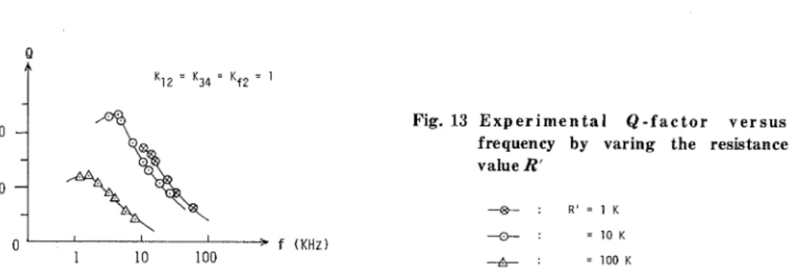
Fig.12 show how the condition И亀4コ【力=l fOr realizing the inductance effects the O‐ factor. K12 ・ K34 = Kf2 ・ 1
R'=10K
Reports of the Faculty of Engineeirng,TOttOri University,V01.13
Fig,13 Experimenta1 0‐ factor versus
frequency by varing the resistance valuc 4′ f (KHz) … : 引 Э― : ― : RI=lK =10K = 100 K
It is clear frona the figure that values of r亀4 and Xtt arOund unity are recommended to achieve high O‐ factor.
Fig, 13 shows the O vs frequency characteristics for various i配 径.In order to obtain a high
O‐factor it is neccessary to keep the resistance翼′around 10 kΩ.
Asis clear from above,O depends on many element values.ヽlhen、ve design the inductance
with moderate O at a given frequency,we must select a suitable combination of element
values to satisけ the specficatiOns.
5.Highpass ladder alters
ln this chapter,、ve deal with the design91'10)。 f5th‐order Butterworth highpass filter and 5th‐
order l dB ripple Chebyshev highptts filter.The inductance in highpass ladder filter is
replaced by the sirnulated inductance.
Fig. 14 is conventional the 5th‐ order Butterworth lowpass filter。 9)「rhe normalizcd element
values of an equally terminated 5th‐ order Butterworth lowpass filter are Rsι =RLι
=lΩ
,と1ゼ=L51=Q・
168H C21=Ql=1.618F and
上31=2H TO transform the normalized lowpass
filter circuit to a highpass configulation, replace each inductance with capadtance and ce versa using reciprocal element values as shown in Fig.15.Then, fOr realizing the
corresponding active highpass filter with a cutOff frequency of 20.01(Hz and an impedance leve1 0f 300 Ω,the foliowing component values are obtained i Rsた こRL´三300Ω ,Gれ
=Cヵ
=
0.043 μF, L2カ 三L4々=1・
482H,(兆
ヵ=0.013 μF.For example, the resistance values
corresponding to inductance value L2カ 三三L4れ,uSing μA 747ど弘3‐type 9p amp with gain
lbandwihth prodttct Gβ
=2π l.5・ 106筋
′
/seC fOr pOwer supply vottage± 15 V,
Clh C2h C5h
5 4
・ Masaru ISHIDA and Hiromu TAFUJI and
Grounded lnductance Using an Operational
Yutaka FUKUf and Keisuke EBISUTANI:A
Amptter POle 4nd ltS Application to Filters
Clh
Fig。 16 Experunental circdt of highptts ladder filter
are R=R3=R4=買
′=10 kΩ
and R2=■
′=100 kΩ
.The inal filter circdt is given in fig. 16.The 5h‐ order l dB ripple Chebyshev filter is reHzed in the sarne manner as above. The normalized element values of an equally terminated 5th‐ order Chebyshev lowpass filter9)are
RSi=RLl=lΩ
,と
11三L51=2.2072H,61=Cl=1,1279 F and」
曳ェ=3.1025 H in Fig。14.The
corresponding active highpass filter with a cutoff frequency of 28.5 KHz and an unpedance level of 300Ω,has the following element values:R説=買
L力=300Ω
,Clれ=G説 =0.0084
μF,L2れ
=と
4ね=1・48躍
H and C挽=0.006
μF.The resistance values COrresponding to inductancevalues L2カ and L4カ are the same as in the exarnple adove Then, the final filter circuit is
gcin(DB)
f(KHz) f(KHz)
10 llXl
(DB)
gcin
Experとnenttl frequenty response of
5th‐order Butterworth highpass f■ ter
10 1∞
Fig,18 Experunenttl frequency response of
5th‐order l dB ripple Chebyschev
highpatt filter
Reports Of the Faculty of Engineeirng, frOttori x」 niversity,VOl. 13 55
shown in Fi富 。16.
These highpass f■ters were composed of μ
4 747〆
て井type op amps with bain gandwidth
product Gβ=2π
l.5・ 106密ヴ//sec and l percent tOlerance resistOrs and capacitances.The power supply voltage is± 15ヽ「.It iS Seen that the experilnental results agree approxirnately、
vith theoretical as is evident from the Figs. 17 and 18 We can conclude from the
experirnenatl described above that the inductance sirnulation circuit shown in Fig.l operates succesfuly as a inductance.
6。 Conclusion
We have described the grounded inductance using op amp pole,The structure sirnulates as inductance and a resistance in series with a capacitance and can be operated at much higher frequencies than classical active network.The circuit is suitable for microcircuit fabrication
of the net、vork.Furthermore,it has been obvious that the reaHzed circuit has lo、v sensitivity
to active and passive elements froni the settsitivity analysis,and the inductance value can be
changed
、vith the resistance ratios 頚儡2, r亀4 and
し , WhiCh assures better temperatureperformance.The proposed circuit is suitable for realizing inductance with rdatively low O‐ factor.The O‐ factor can be adjusted by either the resistance ratios or values.As examples of apphcation of such sirnulated inductance,the 5th‐ order Butterworth and 5th― order l dB
ripple Chebyschev highpass laddeF filter were presented.It has been obvious that these filter configulations work succesfu■ y over the wide frequency.
We expect that this proposed scheme can be readily applied to other filter realizations,
FDNR and GIC ioe.
References
l)Michael A.S:“
Design of act e R filters using only resistors and operational amplifiers'',INT.J ElectrOnics,Vol.40,NO. 5, pp.417--432, 1976.2)J R.Brand and R Schaumann :“ Active R filters i review of theory and practice",Electric Circuits and
Systems,Vo1 2,No 4, pp 89--101, 1978,
3)A.K,Mitra and V,K Aatre:“ Low sensitivity high‐ frequency active R filters",IEEE Trans Circuits and
Systems,Vol CAS-23, No ll, pp 670--676,1976
4)Siddigi M A and Ahmed M.T :“ Realization of gl ounded capacitor with operational amplifiers and
resistance'l Electro.Lett,,Vol 14,No 19,pp.633-634,1978
5)AHen」
,Gumussoy M and Holt A G 工 :``Inductance simulation and filter design usilag a singie・ poleamplifier approxinaation",Electro Lett,Vol 14,No 19,pp 629-631,1978
6)Ananda Mohan P V :``Novel active niters using amplifier p。 le'',Electro lett.,Vol 16,No.10,pp.378 --380, 1980
7) I IShida,T Hirano,Y Fukui and K Ebisutani.:“ A new integrator using Operational amphfier pole",
Rep Fac Eng Tottori Univ,Vol 12,No.1,pp 109-117 0ct,1981
8)L P,Huelsman and P E Alen :``Introduction to the theory and design Of active fnters",Mcgraw‐ Hill, pp 102-133, 1980
9)B
ヽVilhams :“ Electronic flter design handbook", lcgraw‐HiH,Chap 4 and Chap.12,198110)1l J Blinchihoff and A I Zverev :“ Filtering in the time and fl・equency domains",JOhn lVJey&Sons, pp 153-167,1976