Thermal Radiative Characteristics of Nanostructured Tungsten
at High-Temperature
ナノ構造表面を持つタングステンの高温での熱放射特性の向上 髙村 秀一1,上杉 喜彦2,菊池 祐介3,永田 正義3,山田 耕平4,小林 孝裕4,前中 志郎4, 藤田 和宣4,栗下 裕明5Shuichi TAKAMURA1, Yoshihiko UESUGI2, Yusuke KIKUCHI3, Masayoshi NAGATA3, Kohei
YAMADA4, Takahiro KOBAYASHI4, Shiro MAENAKA4, Kazunobu FUJITA4, Hiroaki KURISHITA5
Abstract Fiber-form nanostructure grown on tungsten (W) surface has an excellent thermal radiative property at relatively low sample temperature up to 1200℃. Requirement of maintaining the above radiative property at higher temperature promotes an examination on recovery or annealing characteristics of nanostructured W surfaces, making an emphasis on dopant effect. TFGR-W-1.1%TiC/H (Toughing, Fine-Grained Recrystallized Tungsten with TiC dispersoid) was found to have best characteristics among tested doped W. However, it was noted and discussed that a further improvement at higher-temperature needs an additional processes.
1. Introduction
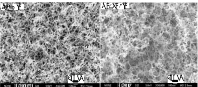
Fiber-form nanostructure on tungsten (W) surfaces has been investigated mainly in fusion science community since its discovery1), 2). It has a very curious morphology, as shown in Fig.1, and properties because entangled W fibers with a few tens nanometer in thickness containing helium (He) bubbles inside show complicated three-dimensional structure, which has been called “fuzz”. The structure has a wide range of spatial characteristic length corresponding to UV-Vis-NIR photon wavelengths and an effectively large surface area compared with macroscopically geometric dimension. Apparently it is a truly black in color visually, suggesting an ideal black-body. Thermal
1 Faculty of Engineering, AIT, Toyota 470-0392 2 Kanazawa Univ., Kanazawa 920-1192
3 Univ. Hyogo, Himeji 671-2280 4 YUMEX Inc., Himeji 671-2114 5 Tohoku Univ., Oarai 311-1313
radiation property was investigated by using electron-beam power source up to 1200 K for a standard PM-W (Powder Metallurgy Tungsten)3). At these temperatures the main light-wavelength range for black-body radiation is from 1.5 through 4.5 m. Figure 1 shows top views with FE-SEM of typical surface morphology for two kinds of W materials. Both structures are almost identical.
Such an excellent radiation capability and surface area enhancement may lead to the following industrial applications: enhancement of cooling capability for electrodes of arc discharge lamps like Xenon (& or
Fig.1 Surface morphologies of W materials exposed to He plasmas. Top views of (a) PM-W, (b) TFGR-W-1.1%TiC/H.
2010_10_22 100 nm (a) PM-W 2010_7_5 100 nm (b) TFGR-W
Mercury) short arc lamp4), solar energy absorber, catalytic materials5).
However, fuzzy structure on W surface disappears at high-temperature, say more than approximately 1500 K, reported in reference 6) where precise temperature measurement of W samples was not carried out. Therefore, a temperature dependence of annealing or recovery of fuzzy W surface should be studied. Moreover, an effort to maintaining such a nanostructure at high-temperature will be required in terms of pinning against growth of grain size due to recrystallization.
Figure 2 shows temperature dependence of W total emissivity which appears at Stefan-Boltzmann law. For example, t = 0.25 at T = 2000 K for pristine W. If black-body radiation capability would be kept at this temperature, then four times increase in radiative power should be obtained.
2. Dependence of Annealing Temperature on Nanostructured Tungsten Surface
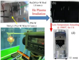
For an accurate temperature measurement of W sample in vacuum, a special capsule made of molybdenum (Mo) was employed as shown in Fig.3, and heated with RF induction coil as shown in Fig.3(c). The capsule is supported inside a glass cylinder which is connected to an evacuation system. W samples set at the capsule are assumed to have a thermal equilibrium with Mo capsule so that the W samples may have the same temperature as Mo capsule whose temperature has been measured with radiation thermometer. A relatively low-temperature like 1000 ℃ gave no substantial
morphological changes as compared between Figs.3(b) and (d).
An example of a higher-temperature annealing (1300℃, for 60 min.) with the same RF induction heating system is shown in Fig.4, indicating an almost complete recovery of some W alloys. Therefore, we understand that a critical temperature would be located between 1000 ℃ and 1300 ℃ , corresponding to recrystallization temperature of 1200℃ for pure W.
Fig.2 Temperature dependence of total emissivity t.
Fully nanostructured black W has almost ideal black-body property over a wide temperature range.
Fig.3 Low-temperature annealing in vacuum: W samples on PM-W sheet (a) before (b) after He plasma exposure, (c) during annealing with radio-frequency induction heating (183 kHz), (d) Photo of W samples set on Mo capsule after annealing.
Fig.4 High-temperature annealing in vacuum: (a) W samples set on Mo capsule after annealing at 1200℃ for 60 min, (b) RF induction heating (183 kHz) at 1300℃, (c) photo of W samples after annealing at 1300℃ for 60 min.
A drastic morphological change from 1200°C to 1300℃ is summarized in Fig.5 for PM-W sheet, ThO2 (1.5%) doped W thin wire and Re (26%) + W alloy wire. But still there are some differences among several kinds of W compounds.
3. Tungsten Solid Solution and Doped Tungsten
There would be still some questions about a complete thermal equilibrium between the Mo capsule and W samples inside, and a uniformity in temperature over the W samples with RF induction heating system introduced in the previous section. In order to obtain a more reliable control of sample temperature, a vacuum furnace shown in Fig.6 has been employed, in which a resistive heating and temperature measurement with a thermocouple provide a programmed temperature rise and maintaining constant temperature followed by a natural cooling as shown in Fig. 6.
Figure 7 shows the photo of several W samples (a) before and (b) after 1300℃ - 60 min annealing. This is called as the standard annealing condition. Visually, ThO2 doped W and TFGR-W1.1%TiC/H (Toughing, Fine-Grained Re-crystallized Tungsten with TiC dispersoid)7)~10) samples show incomplete recovery, understanding from gray in surface color compared with pure W wire, W + Re(26%) alloy wire and PM-W
sheet. Annealed surface morphologies of
TFGR-W1.1%TiC/H are shown in Fig.8 with four kinds of magnifications in FE-SEM. It keeps some nanostructure on the surface although thin and long W-fibers are shortened and become fat.
Fig.5 Changes in surface morphologies of several W samples exposed with He plasma by annealing on 1200℃ for 60min and additional 1300℃ for 60 min.
Fig.6 Standard temperature history of SHIMAZU annealing furnace in vacuum and its front view.
Fig.7 Several W wires and TFGR-W1.1%TiC/H sample on PM-W sheet: (a) after He plasma exposure, (b) after the standard annealing.
Fig.8 Surface morphology of TFGR-W1.1%TiC/H after the standard annealing, (a) ~ (d) FE-SEM images with different magnifications and view angles.
Grazing view @ 40°1 m (b) Grazing view @ 35°1 m (c) Grazing view @ 40°10m (d) 1 m (a) Top view
On the other hand PM-W sheet loses almost completely fiber-form nanostructure, as shown in Fig.9 (a), while pure W wire with 0.5 mm in diameter leaves vestiges of W-fibers, probably due to drawn-working process for fabrication of thin W wire.
Figure 10 gives a comparison of surface morphologies between W + Re (26%) alloy and Re (3%) doped W thin wires with 0.5 mm in diameter. Solid solutions composed of W and Re does not have
any effects on annealing property, while a small amount of Re doping would have certain influence because the dopant inserted into grain boundaries may have a pinning role against grain growth according to temperature increase11). This mechanism may be also the case for ThO2 (1.5%) doped W, as shown in Fig.11.
In gas discharge lamp industry, many kinds of doped W have been employed for various kinds of electrode materials4). Potassium (K) doped W (so-called EX-W by A.L.M.T. Corp.)12) is one of examples for lamp
electrode ensuring good manufacturing and
anti-deformation properties. The recrystallized temperature is known to be increased with this processing. The annealed surface seems to be identical to the pristine one visually, as shown in Fig.12 (a). The detailed FE-SEM images shown in Fig.12 (b) ~ (d) indicate an incomplete recovery of W surface, leaving
Fig.9 Surface morphologies of PM-W after the standard annealing, (a) PM-W sheet, (b) PM-W wire with 0.5 mm in diameter. 2016_2_22 2016_3_16 1 m 2016_2_22 2016_3_16 1 m Grounding PM-W (a-1) (a-2) 1 m 1 m Pure W Wire 0.5mm (b-1) (b-2)
Fig.10 Surface morphologies of Re-W compound after the standard annealing, (a) solid solution of Re (26%), (b) Re (3%) doped W thin wire.
10 m He exposure on 2016_2_22 Annealing on 2016_3_16 (a-1) 1 m (a-2) 10 m He exposure on 2016_4_8 Annealing on 2016_4_19 (b-1) 1 m (b-2)
Fig.11 Surface morphologies of ThO2 (1.5%) doped W after
the same annealing as in Fig.10.
1 m 10 m
(a) (b)
2016_2_22:He exposure 2016_3_16: Anneal
Fig.12 Surface morphologies of K (33 ~ 55 ppm) doped EX-W. (a) photo showing a change in surface due to the same annealing as Fig.10, (b) ~ (d) FER-SEM top views.
vestiges of W nano-fibers. Another doped W, WL-S which is fabricated by doping lanthanum oxide (La2O3 1%)13) is said to be resistant to breakage even after high-temperature processing. FE-SEM images after the same annealing of black WL-S with He plasma exposure are shown in Fig.13. Vestiges of W nano-fibers are more apparent than the case of EX-W.
The above experimental investigations suggest, as one of clues, dopant inserted into grain boundaries against grain growth due to temperature increase as is schematically shown in Fig.14. This mechanism has been used for the manufacturing process to increase re-crystallization temperature to enhance mechanical properties.
Figure 15 shows diffuse reflectance for several W
surfaces over a wide radiation-wavelength,
UV-Vis-NIR. The measurement was performed with SHIMAZU SolidSpec-3700 which employs BaSO4 powder as a reference of 100% reflectance. Before annealing, a fiber-form nanostructured black PM-W exposed by He plasma shows at most 5% reflectance over whole range, meaning really a black-body. Here, (, T) = 1.0 – r(, T), where (, T) is the spectral emissivity, and r(, T) is the spectral diffuse reflectance. Annealed TFGR-W1.1%TiC/H has reflectance of an approximately half of pristine PM-W material, due to leaving some vestiges although it would not be satisfactory for enhanced cooling capability of lamp electrode and other industrial and scientific applications14).
4. Summary
Fiber-form nanostructured W surface has a thermal radiation capability of an almost complete black-body, meaning total emissivity t(T) = 1.0 under the surface temperature less than 1100 ℃ which is close to re-crystallization temperature of pure W. This was confirmed by a power balance experiment between electron beam power input and thermal radiation loss. Morphologies of fiber-form nanostructures grown on doped W material surfaces are found to be the same as those on pure W.
Fig.13 Surface morphologies of La2O3 (1%) doped WL-S after the same annealing as in Fig.10.
1 m (b) 1 m (c) 1 m (d) 10 m (a)
La2O31% doped Tungsten (WL-S) He exposure on 2016_5_24; Annealing on 2016_6_7
Fig.14 Model for doped material role.
Fig.15 Diffuse reflectance on wide wavelength range with UV-Vis-NIR spectrophotometer.
Above the re-crystallization temperature for pure W, surface changes due to the annealing for 60 min at 1300℃ from fuzzy surface have been examined for not only pure W but also doped W alloy including solid solutions. Rolled-work W sheet and drawn-work W thin wire made of pure W were studied and found that fiber-form nanostructure disappears with a small
difference between pure W with different
manufacturing processes.
Among several doped W materials,
TFGR-W1.1%TiC/H was found to show the best thermal radiation property after the annealing of 60 min at 1300 ℃ . This was confirmed with FE-SEM observations and diffuse-reflectance measurement. TFGR-W3.3%TaC/H has similar characteristics, although not shown here. La2O3(1%) doped WL-S was secondary, and Re(3%) doped W and ThO2(1.5%) doped W follow the above. On the surface of K(33~55 ppm) doped EX-W annealed at the same conditions as the above, vestiges, fat and shrunk W-fibers, are left. These findings show the role of dopant inserted at grain boundaries, contributing pinning against grain growth at high-temperature. However, solid solution like Re (26%) + W alloy does not show any improvement of maintaining nanostructure on surfaces. In spite of the above investigations, doping procedure is not enough to reserve a high radiation property as well as an enhancement of effective surface area. We have to explore different approaches which are open to be studied in future. For example, LIPSS (Laser Induced Periodical Surface Structure)15) with femto second laser should be tested. In addition micron-sized laser marking technique on doped W surface before He plasma exposure is one of other possibilities.
Acknowledgements
The work is supported by the Japan Society for the Promotion of Science, Grant-in-Aid for Scientific Research (C) 26420855. The author (S. Takamura) thanks Mr. S. Ono of Tamari Industry Co., LTD for discussions on laser applications.
References
1) S. Takamura et al., “Formation of Nanostructured Tungsten
with Arborescent Shape due to Helium Plasma Irradiation”, Plasma Fusion Res. Vol.1, 051 (2 pp), 2006.
2) S. Takamura and Y. Uesugi, “Experimental identification for physical mechanism of fiber-form nanostructure growth on metal surfaces with helium plasma irradiation”, Appl. Surf. Sci. Vol.356, pp.888-897, 2015.
3) S. Takamura, “Radiative cooling properties of he-defected tungsten with fiber-form nanostructured surface”, J. Nucl. Mater. Vol.466, pp.239-242, 2015.
4) http://yumex-inc.co.jp/en/
5) S. Kajita, T. Yoshida, D. Kitaoka, R.Etoh, M. Yajima and N. Ohno, “Helium plasma implantation on metals: Nanostructure formation and visible-light photocatalytic response”, J. Appl. Phys. Vol.113, 134301(7pp), 2013,
6) T. Miyamoto, S. Takamura and H. Kurishita, “Recovery of Tungsten Surface with Fiber-Form Nanostructure by Plasma Exposure”, Plasma Sci. Technol. Vol.15, pp.161-165, 2013. 7) H. Kurishita, S. Matsuo, H. Arakawa, T. Sakamoto, S. Kobayashi et al., “Development of re-crystalized W-1.1%TiC with enhanced room temperature ductility and radiation performance”, J. Nucl. Mater. Vol.398, pp.87-92, 2010. 8) H. Kurishita et al., “Development of Nanostructured Tungsten Based Materials Resistant to Recrystallization and/or Radiation Induced Embrittlement”, Mater. Trans. Vol.54, pp.456-465, 2013.
9) H. Kurishita et al., “Current status of nanostructured tungsten-based materials development”, Phys. Scr. Vol.T159, 014032(7pp), 2014.
10) M. Zibrov, M. Mayer, L. Gao, S. Elgeti, H. Kurishita et al., “Deuterium retention in TiC and TaC doped tungsten at high temperatures”, J. Nucl. Mater. Vol.463, pp.1045-1048, 2015.
11) R.P. Simon, G.J. Dooley and T.W. Haas, “Study of Grain Boundary Fracture Surfaces in Doped Tungsten-Rhenium Alloys”, Mater. Trans. Vol.5, pp.585-591, 1974.
12) http://www.allied-material.co.jp/english/ 13) https://www.plansee.com/en/index.html
14) J. Nakamura et al., “Optimal crossed overlap of coherent vacuum ultraviolet radiation and thermal muonium emission for SR with the Ultra Slow Muon”, J. Phys.: Conf. Series, Vol.551, 012066(6pp), 2014., 2006.
15) B. Tan and K. Venkatakrishnan, “A femtosecond laser-induced periodical surface structure on crystalline silicon”, J. Micromech. Microeng., Vol.16, pp.1-6, 2006.