Surface Studies on Quasicrystals and
Creation of Single Element Quasicrystals
Masahiko Shimoda1,* and An Pang Tsai1,2
1 National Institute for Materials Science, 1-2-1, Sengen, Tsukuba, Ibaraki 305-0047,Japan 2 Institute of Multidisciplinary Research for Advanced Materials, Tohoku University,
Sendai 980-8577, Japan SHIMODA.Masahiko@nims.go.jp
Studies on the surface structure of an icosahedral quasicrystal and on thin film growth on a quasiperiodic substrate are presented. Scanning tunneling microscopy (STM) images from the fivefold surface of icosahedral Ag-In-Yb quasicrystal show a step-terrace structure of an aperiodic sequence of steps with different heights. For
higher resolution images, characteristic local structures of atoms are observed commonly on any terraces. From a comparison of these findings with the bulk structure of icosahedral Cd-Yb quasicrystal, an isostructural material to Ag-In-Yb quasicrystal, it follows that the surface termination perpendicular to the fivefold axis occurs at planes intersecting centers of the atomic cluster, the building unit of quasicrystals. Pb deposition on the fivefold surface gives rise to the growth of Pb layers with quasiperiodic structure. STM observations and first principle calculations reveal that the atomic structure of the Pb film is the same as that of the substrate. This is the first step toward the realization of the single element quasicrystal.
Keyword: quasicrystal, fivefold surface, thin film, single element quasicrystal
Masahiko Shimoda was born in Osaka, Japan, and graduated from Kyoto University in 1979. After joining in National Research Institute for Metals (present National Institute for Materials Science) in 1984, he received his PhD in 1986 at Kyoto University. His main research interests are in the surface structure of quasicrystals and thin film growth on the quasiperiodic planes.
An-Pang Tsai is a professor at Institute of Multidisciplinary Research for Advanced Materials (IMRAM), Tohoku University and also a research advisor of Center for Green Research on Energy and Environmental Materials at National Institute of Materials Science (NIMS) in Japan. He received Doctor of Engineering from department of materials physics at Tohoku University in 1990. His research interests include formation, structure and application of quasicrystalline alloys. He is also studying catalysts aiming at designing new type catalysts which might be able to replace precious metals, in terms of controlling electronic structure and microstructure of alloys.
準結晶の表面および単元素準結晶の創成
下田正彦1、蔡安邦1,2 1, 物質・材料研究機構, 2 東北大学多元物質科学研究所 1. はじめに 金属間化合物のなかには、準結晶と呼ば れる一群の物質が存在する。準結晶は、通常 の周期結晶のような並進対称性を持たないが アモルファスのようにランダムでもなく、複雑で はあるが高い秩序構造(=準周期構造)をも つ物質である[1]。その特徴は、結晶では有り 得ない回転対称性(例えば 5 回回転対称)を 持つことである。1984 年に D.Shechtman(2011 年ノーベル化学賞受賞)らによって発見[2]さ れて以来、今日までに 100 を超える合金系で 準結晶が見つかっている。 準結晶は物性においても特異な特性を示 し、金属にしては高い電気抵抗率や熱起電力 を示すもの、半導体的な抵抗の挙動を示すも のが存在する[3]。最近では、強相関電子系の 準結晶で新しい量子臨界現象が発見され、活 発に研究されている[4]。このような物性には、 準周期構造が強く関連していると考えられる。 しかし、周期性がない準結晶では構造を決定 することが大変難しく、それが物性発現の機 構を解明する上で大きな障害となっている。 一般に、準結晶のバルクの構造は、電子顕 微鏡などで得られる原子像あるいは組成の近 い結晶相の構造を元に、モデル構造を構築し、 これを出発点として観測された回折像が再現 される構造を探索することで得られる。 準結晶の表面研究の目的の一つは、得ら れた構造の妥当性を検証することである。そ のためには、観察された表面の原子像やステ ップ-テラス構造をモデル構造と比較すること が必要となる。さらに、準周期構造に特有な物 理現象を、表面を利用して明らかにすることも 重要なテーマである。すなわち、準周期構造 というエキゾティックな基板を舞台に、原子や 分子がどのように振る舞うか、吸着や膜成長を 通じて解明することである。中でも興味深いの は、エピタキシャル成長による単元素準結晶 薄膜の作製である。単元素準結晶とは、1種 類の元素からできた準結晶のことである。実は、 これまでに知られている準結晶のほとんどは3 元以上の合金であり、その化学的な複雑さが 準結晶の理解を困難にする要因の一つであ る。そこで化学的に単純な準結晶を、表面を 利用して作ることで、準結晶の安定性の起源 解明や、準結晶構造に特有な物性を明らかに しようというのが単元素準結晶作製の狙いで ある。 準結晶の表面研究は、その発見直後から 始まったが、熱力学的に安定な準結晶が発見 されて以降、良質な単相の試料が得られるよ うになり大きく進展した[5-7]。中でも正 20 面体 相の準結晶は、最も詳しく調べられている。 正 20 面体相の準結晶は、正 20 面体の対称 性を持ち、5、3、2 回の回転対称軸がそれぞ れ 6、10、15 本存在する。表面の研究で対象 となるのは、主にこれらの回転対称軸に垂直 な対称性の良い面である。そのような面の方 位は、回転対称軸の方位で示し、例えば 5 回 対称軸(fivefold axis)に垂直な表面を 5 回面 (fivefold plane)と呼ぶ。 本稿では、正 20 面体相 Ag-In-Yb 準結晶 [8]について、その清浄 5 回面の構造および単 元素準結晶作製を目的とした 5 回面上の Pb 薄膜の構造と成長について紹介する。 2. Ag-In-Yb 準結晶と Cd-Yb 準結晶 Ag-In-Yb 準結晶は、正 20 面体相 Cd-Yb 準結晶[9]から、1原子あたりの価電子数が変 化しないように Cd を等量の In と Ag で置換す ることで得られる。Cd-Yb 準結晶は、2元合金 系で初めて見つかった準結晶で、現在に至る まで構造の詳細が明らかになっている唯一の 準結晶である(化学的に単純化されたことで準結晶の研究が進展した典型的な例である)。 ただし、蒸気圧の高い Cd を含むので、超高 真空中で熱処理が必要な実験には不向きで ある。そこで表面研究には、これと同じ構造を もち熱処理の問題もない Ag-In-Yb 準結晶が 使われる。なお、本稿では Ag-In-Yb 準結晶 について議論するが、構造に関しては Cd-Yb 準結晶のデータをそのままを用いる。 3.クラスター構造 一般に結晶の構造は、結晶格子と各格子 点を修飾する基本構造とで記述される。これ に対し、準結晶の構造は、準周期格子とその 格子点を修飾する原子クラスターとで記述さ れる。正 20 面体相準結晶の場合、準周期格 子は 3 次元ペンローズ格子とよばれるもので、 2種類の菱面体で空間を隙間なく埋めた構造 になっている[10]。 原子クラスターは個々の準結晶に固有で、 Cd-Yb 準結晶の場合、5 重の殻構造をもつ (Figure 1)[9]。これは Tsai 型クラスターと呼ば れるもので、その特徴は、第 3 殻の 20 面体の 各サイトが Yb だけで占められており、他の4つ の 殻 に は Yb は 存 在 し な い こ と で あ る 。 Ag-In-Yb 準結晶でも同様で、第3殻は Yb で 占められており、他の殻は In と Ag で構成され ている。なお、厳密にはクラスターに属さずク ラスターとクラスターの隙間に存在する原子も あるが、その割合は僅かなので本稿の議論で は無視する。 4. 清浄準周期表面 Ag-In-Yb 準 結 晶 の 単 相 試 料 は 、 Ag42In42Yb16の仕込組成で Bridgman 法により 作成される[11,12]。得られた試料を5回対称 軸に垂直に切り出し、表面を研磨して5回面を 得る。このとき得られたラウエ像から、この試料 が正 20 面体の対称性を示し、しかも極めて良 質の単相であることが確認できる(Figure 2)。 清浄表面を得るには、表面の酸化物層を取 り除く必要がある。そのため、超高真空中で、 Ar イオンスパッタリングとアニールを繰り返し 行う[13,14]。このとき、X 線光電子分光(XPS) で表面の組成をモニターする。Yb の酸化物は 安定で、しかもアニール中に試料やその周辺 から放出されるガスによっても容易に酸化され てしまうので、Yb 酸化物の信号が十分小さく なるまで繰り返す必要がある。 一般に化合物のスパッタリングでは、元素 によってスパッタされる割合が異なる選択スパ ッタリングが問題となる。Ag-In-Yb 準結晶の5 回面の場合、スパッタリングによって表面付近 の In の割合が大幅に減少するが、アニール することによりバルクの組成が回復することが
Figure 1. Tsai-type cluster of Cd-Yb quasicrystals. The five sub-shells are, from inside to outside, a tetrahedron of 4 Cd atoms, a dodecahedron of 20 Cd atoms (diameter of the circumscribed circle=0.86 nm), a icosahedrons of 12 Yb atoms (0.11 nm), an icosidodecahedron of 30 Cd atoms(0.13 nm) and a rhombic triacontahedral with 92 Cd atoms (0.16 nm).
Figure 2. Back Laue X-ray diffraction patterns for a single-grain Ag–In–Yb quasicrystal taken with incidences along the (a) 2-fold, (b) 5-fold and (c) 3-fold axes. Reproduced from Ref. 11.
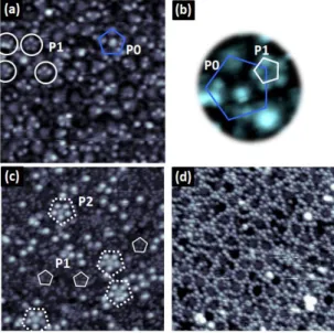
XPS で確認された(Figure 3)。また、スパッタリ ングによって乱れた構造は、アニールによっ て回復し5回対称の長距離秩序が復元される ことが表面の回折像から確かめられた(Figure 4)[13,14]。こうして得られた表面が、清浄な5 回対称表面(5回面)である。 5. 5 回面の構造 Figure 5 は、Ag-In-Yb 準結晶の 5 回面の走 査型電子顕微鏡(STM)像である[14]。μm ス ケールの広いテラスを持ったステップ-テラス 構造が見られる。特徴は、テラスの直下のステ ップの高さがテラスごとに異なることである。こ の図に示す範囲では、L~0.85 nm、S~0.28 nm の2種類のステップが LSLSS の順に現れて いる。L の前後は必ず S であるが、S は連続し て現れるのが特徴である。 テラスの構造を原子レベルのスケールで観 察したのが Figure 6 である[15]。2つの STM 像 は、スケールはほぼ同じだが、試料に印加さ れるバイアス電圧はそれぞれ、(a) -0.81 V、(b) +0.95 V と異なる。すなわち、バイアス電圧の 極性によって全く異なった像が観測される。 負バイアスの像(Figure 6(a))では、一見不規 則な位置に輝点が観測されるが、よく見るとこ れらの多くは正 5 角形の位置関係にあること が判る。以下ではこの正 5 角形を P0 とする。 P0 の一辺の長さは、~2.40nm であり、これは
Figure 3. The intensity ratio of Ag 3d5/2, In 3d5/2 and Yb 4d5/2 core-level photoemission from the fivefold surface of Ag–In–Yb quasicrystal after sputtering and the following annealing. Bars on the right show ideal intensities for Ag44In44Yb16.
Figure 4. (a,b) RHEED images from the fivefold surface of Ag-In-Yb quasicrystal, (a) after sputtering and (b) after annealing at 200 oC. The large and strong spot is due to a reflection from objects other than the sample.Reproduced from Ref 13. (c) LEED pattern from the same surface after annealing at 400 oC (electron energy: 23.4 eV).
Figure 5. A large scale STM image of the fivefold surface of Ag-In-Yb quasicrystal. Reproduced from Ref 14.
クラスターの最外殻の直径よりも大きい値であ る。従って、これら輝点は個々の原子に対応し ているのではないと考えられる。 一方、正バイアスの像(Figure 6(b))では、よ り微細な構造が見える。特徴的なのは、正 5 角形や環状に並ぶ輝点が随所に見られること である。正 5 角形を花びら(Petal)に見立てると、 5 弁花(Five-Petaled Flower, FPF)のような局 所構造が認識できる(Figure 6(c))。Petal の辺 の長さは~0.56 nm であるので個々の輝点は 原子に対応していると考えられる。FPF は、完 全な形で現れる場合もあれば、Petal が一部 欠けた不完全なものもある。隣の FPF との関 係は、一つの Petal を共有することもあれば、 Petal が無く接する場合もあるなど、リンクの仕 方には複数のパターンがある。 こうした観測結果をモデル構造と比較すると き問題になるのは、準周期構造では、ある特 定の面と完全に同一の構造をもつ面は他に 存在しないことである。そのため、観測された 原子像と完全に一致する面を、モデル構造中 に見つけることは、無限に異なるパターンの中 から特定のパターンを探すことになるので、た とえそれが正しい構造だとしても、ほとんど不 可能である。 そこで、原子像全体ではなく、原子像に現 れる特徴的な局所構造(モチーフ)に注目し て構造を比較する。実際、準結晶の表面では、 異なる場所(一つの試料の異なるテラス、別の 試料の表面など)を観測しても、その準結晶に 特有のモチーフが常に現れる。Ag-In-Yb 準 結晶の5回面の場合、そのようなモチーフは P0 の五角形であり FPF である。これらが現れ る面をモデル構造中に探し、得られた面が表 面となったとき、観測されたスッテプ-テラス構 造が再現できるかを検討するのが比較の方法 である。 Cd-Yb 準結晶の構造において、FPF のよう なモチーフを探すと、Figure 7 に示すような面 が見つかる。これは 5 回軸に垂直でクラスター 中 心 を 含 む 面 ( Cluster-center Intersecting Fivefold Plane, CcIFP)である。CcIFP では、 Yb が正 5 角形を成し FPF を構成しているのが 判る。FPF の中心にクラスター中心の一つが 存在する。モデル構造の Petal の辺の長さは 0.60 nm であり、観測された局所構造にほぼ一 致する。 CcIFP には、10 個の Cd サイトが環状(もしく は正 10 角形)に並ぶ構造(Ring)も見える。 Ring はクラスター中心の周囲、FPF の内側に
Figure 6. (a,b) High resolution STM images of the clean fivefold surface of Ag-In-Yb quasicrystal taken at (a) -0.5 V (23 nm x 23 nm) and (b) 0.95 V (20 nm x 20 nm). An example of the P0 pentagon is highlighted in colored lines. The image (b) is processed to enhance fine structures by superimposing a Fourier filtered image. Reproduced from Ref. 15 with permission from The Royal Society of Chemistry. (c) A close-up image of the rectangular region given in Figure 6(b). An FPF motif is highlighted with a ball-stick drawing.
位置する。クラスター中心は、多くの場合周囲 のクラスター中心とともに正 5 角形を形成する。 典型的なのは、Figure 7 の中央に描いた大き な正 5 角形である。この正 5 角形の一辺の長さ は、2.53 nm であり、負バイアスの像の正 5 角 形 P0 (Figure 6(a))に対応していると考えられる。 すなわちこの Ring を含むクラスター全体が 1 個の輝点として観測されるとすれば負バイアス の像が説明できる。 なお、個々の Petal と中心の Ring は、それ ぞれ別のクラスターに属している。各 Petal の 正 5 角形は、Tai クラスター第 3 殻の 5 回軸に 垂直な面にある 5 つの Yb に対応しており、そ のクラスター中心は別の面上にある。また、 Ring の 10 個の Cd は、すべて一つのクラスタ ーの第 4 殻に属し、その中心が CcIFP を成し ている。 このような CcIFP が最表面であるなら、ステ ップは CcIFP の間隔に対応するはずである。 これを確認するために、CcIFP の出現する位 置を、5回軸に沿っての原子密度分布上に示 したのが Figure 8 である。原子密度は、Cd-Yb 準結晶の充分大きな構造データを用意し、こ れの5回軸に垂直な厚さ 0.02nm の層での平 均原子密度を 0.005nm ごとに計算して求めた。 隣接する CcIFP の間隔に注目すると、L~ 0.81 nm、S~0.27 nm の2種類ある。その出現 の仕方は、L の隣は必ず S で、S の隣は L また
Figure 7. Atomic structure of CcIFP extracted from the model structure of Cd-Yb quasicrystal (50 nm x 50 nm). Cd, Yb and the center of cluster are displayed in red, green and grey dots, respectively. Structures corresponding to the P0 pentagon and the FPF motif are marked with lines.
Figure 8. Relative atomic density along the fivefold axis (red: Cd, green: Yb, black: total, blue: cluster centers). The density is evaluated with the average within a layer of 0.02 nm in thickness. The maximum projected atomic density in this region is comparable to that of the closed-packed Yb surface. The position of the cluster centers is marked by arrows.
は S となっている。従って、CcIFP の間隔は、 観測されたステップの高さ・順列とよく対応し ている。なお、Figure 8 から判るように、CcIFP の特徴は、局所的に原子密度が高いうえ、全 原子密度に対する Yb の密度が相対的に高い ことである。従って、Yb 間の結合が強いことが 安定な表面に大きく寄与していると推測され る。 以上のことから、5 回面は Yb の相対密度が 高い CcIFP で終端すると結論される。また、観 測精度の範囲内では、表面に再構成や緩和 は認められず、バルク終端であると言える。 STM 像がバイアス電圧の極性に依存すること は、フェルミ面近傍の状態密度の違いで説明 されている[16]。 6. 5 回面上の Pb:単元素準結晶薄膜 前項で見たように、Ag-In-Yb 準結晶の 5 回 面は、Yb の FPF と Cd サイト(Ag-In-Yb 準結 晶では In または Ag)の Ring に対応する P0 を モチーフとする準周期構造の表面であり、 Ring の属するクラスターの中心を通る CcIFP で分割されて現れる構造が、最表面として露 出している。そこで、単元素準結晶薄膜のエ ピタキシャル成長の試みとして、この面に Pb 原子を蒸着し、蒸着量とともに成長する Pb 層 を観察した[17]。単体としては高い超伝導転 移温度を有する Pb を用いて、準周期構造に より超伝導特性がどのような影響を受けるのか 調べるのが狙いである。 蒸着初期の表面では、Pb は下地からの高 さ~0.11nm のところに、1辺~0.92nm の小さ な正 5 角形を形成する(Figure 9(a))。この 5 角 形を P1 とする。この段階では、下地の Ring に 対応する輝点がまだ見えており正 5 角形 P0 も 認識できる。P1 の向きは一定で、この図に見 える範囲では P0 と同方向であり、下地の構造 と相関があることが判る(P0 の選び方次第で逆 方向の場合もある)。実際、P0 の頂点のまわり に P1 が形成されているところを捉えた像も得 られている(Figure 9(b))。 観測された P1 のサイズや P0 との位置関係化 から、吸着した Pb の CcIFP 上での位置は Ring と Petal の 隙 間 に 相 当 す る こ と が 判 っ た (Figure 10(a))。さらに、吸着の高さを考慮する と、吸着サイトはバルクでは Petal が属するクラ スターの第 4 殻の原子位置に相当することが 判った。 さらに蒸着量を増すと、下地からの高さ~ 0.31nm のところに一辺~1.38 nm のより大きな 正 5 角形 P2 が現れる(Figure 9(c))。P2 は P1 と逆向きである。P2 の各頂点は、CcIFP 上で は、1つの FPF に属する Petal と Petal の隙間 に位置する(Figure 10(b))。蒸着がさらに進み、 5 つの隙間がすべて埋まると、各 Petal の中心 の真上があらたな吸着点となり、P2 の正 5 角 形の頂点間が埋まってあたかも正 10 角形を 成すように成長していく(Figure 9(d), Figure 10(c))。こうしてできた正 10 角形をモチーフと するネットワーク状の構造が第2層である。
Figure 9. (a) Formation of the first Pb layer. P0 and P1 features (see text) are marked by a pentagon and circles, respectively (30 nm x 30 nm). (b) A close-up image of the P1 feature formed at the corner of a P0 pentagon. (c) The early stage of the second layer formation. Pb atoms form P2 pentagons (30 nm x 30 nm). (d) A network of Pd decagons forms the second layer (30 nm x 30 nm). Reproduced from Ref.18.
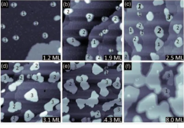
なお、モデル構造との比較から、P2 は、バ ルクでは Petal に接する別のクラスターの第 3 殻のサイトである。また、Petal の中心の真上の 位置は、Petal が属するクラスターの第 3 殻の 一部に相当する。 このようにして形成された第 1 層、第 2 層に ついて、各 Pb 吸着サイトの安定性が第一原 理計算によって調べられた[17]。計算では、 一つの FPF を完全に含む表面近傍の円盤状 の領域を表面とした。計算の結果、清浄表面 においては第 1 層のサイト(P1)が最も安定で あることが確認された。また、第 2 層が成長す るには、第 1 層の完成後、まず下地と第 1 層の 中間の高さにあるサイト(下層サイト)に Pb が 吸着することが必要で、これによって第 2 層の 各サイトが安定化することが示された。この下 層サイトはバルクの構造においてはクラスター の最外殻の一部に相当する。なお、このような 下層の存在は STM では確認できないが、XPS の測定を分析することで確認されている。 このように、実験および計算によって、Pb が 吸着するサイトは、バルクの準結晶であれば、 Yb や Cd が占めているはずであった位置であ ることが判った。このようにして、基板準結晶上 に基板と同じ構造の Pb の多層膜が成長する ことが確認された。これは、単元素からなる 3 次元的な準周期構造としてはじめてのもので ある。 7. Pb 多層膜 Pb 準周期膜の完成後、より厚い Pb 準周期 膜、すなわち Pb の単元素準結晶作製を目指 し、さらに Pb の蒸着を続けた[18]。残念ながら これまでの実験では、準周期構造の物性への 影響を調べられるような充分な厚さを持つ多 層膜は得られなかった。 蒸着を続けると Pb 薄膜は 3 次元的なアイラ ンドを形成して成長する (Figure 11)。蒸着量 を増すに従い、アイランドのサイズが大きくなり 厚さも増す。4.3ML 以上では、アイランド同士 の凝集が始まり、最終的には連続的な膜とな る。ここで、1ML は Pb 準周期膜の完成時の蒸 着量である。これまでのところアイランド表面の 原子像は得られておらず、その構造は不明だ が、エッジが正三角形を成すような成長が見 受けられるので、結晶相だと考えられる。 7. まとめ 正 20 面体相 Ag-In-Yb 準結晶の5回面の構 造および5回面上に成長させた Pb 薄膜の STM 観察について紹介した。清浄な5回面で は、高さの異なるステップが非周期的に出現 するステップ-テラス構造、および特徴的な局 所構造を持った原子像が観測された。これら
Figure 11. STM images of multilayer film of Pb at different coverages, showing Pb islands of different heights. Reproduced from Ref.18.
Figure 10. Schematic views of Pb adsorption sites (white dots) projected on the CcIFP, for (a) the first layer, (b) the initial stage of the second layer and (c) the completed second layer.
の結果をモデル構造と比較し、表面がクラスタ ー中心を含む面(CcIFP)でのバルク終端であ ることを示した。5回面の Pb 蒸着では、STM 像 の解析と第一原理計算による安定吸着サイト の考察の結果、基板の準結晶と同じ構造の Pb の多層膜の成長が確認された。これは、単 元素準結晶実現への第一歩であり今後の進 展が期待される。 8. 謝辞 本稿で紹介した研究は、参考文献の共著者ら との共同によるものであり関係者には深く感謝 する。研究の一部は JST 戦略的創造研究推 進事業発展研究(SORST)の補助を受けて実 施された。 参考文献 1) 竹内 伸,枝川圭一,蔡 安邦,木村 薫:『準結晶の物理』(朝倉書店,2012).
2) D. Shechtman, et al.: Phys. Rev. Lett. 1984, 53, 1951-1953.
3) J. Dolinsek, Chem. Soc. Rev. 2012, 41, 6730-6744.
4) K. Deguchi, S. Matsukawa, N. K. Sato, T. Hattori, K. Ishida, H. Takakura, and T. Ishimasa, Nature Materials 2012, 11, 1013-1016.
5) H. R. Sharma, M. Shimoda and A. P. Tsai, Adv. Phys. 2006, 56, 403-464.
6) M. Shimoda and H. R. Sharma, J. Phys.: Condens. Matter 2008 , 20, 314008. 7) V. Fournée, J. Ledieu, M. Shimoda, M.
Krajčí, H. R. Sharma and R. McGrath, Isr. J. Chem. 2011 , 51, 1314-1325.
8) J. Q. Guo and A. P. Tsai, Philos. Mag. Lett., 2002, 82, 349-352.
9) A. P. Tsai, J. Q. Guo, E. Abe, H. Takakura and T. J. Sato, Nature, 2000, 408, 537. 10) A. L. Mackay: Sov. Phys. Crystallogr. 1981,
26, 517.
11) C. Cui and A. P. Tsai, J. Crystal Growth 2009, 312, 131–135.
12) C. Cui and A. P. Tsai, J. Alloy. Comp. 2012,
536, 91–93.
13) H. R. Sharma, M. Shimoda, S. Ohhashi and A. P. Tsai, Philos. Mag. 2007, 87, 2989-2994.
14) H. R. Sharma, M. Shimoda, K. Sagisaka, H. Takakura, J. A. Smerdon, P. J. Nugent, R. McGrath, D. Fujita, S. Ohhashi, and A. P. Tsai, Phys. Rev. 2009, B80, 121401. 15) C. Cui, H. M. Shimoda, A. P. Tsai, RSC
Adv. 46907 (2014).
16) H. R. Sharma, G. Simutis, V. R. Dhanak, P. J. Nugent, C. Cui, M. Shimoda, R. McGrath, A. P. Tsai, and Y. Ishii, Phys. Rev. 2010, B81, 104205.
17) H. R. Sharma, K. Nozawa, J. A. Smerdon, P. J. Nugent, I. McLeod, V. R. Dhanak, M. Shimoda, Y. Ishii, A. P. Tsai, and R. McGrath, Nature Communications 2013, 4, 2715.
18) H. R. Sharma, J. A. Smerdon, P. J. Nugent, A. Ribeiro, I. McLeod, V. R. Dhanak, M. Shimoda, A. P. Tsai, R. McGrath. J. Chem. Phys. 2014, 140, 174010.