Paper
Auger Electron Spectroscopy Analysis of W diffused from WC
Grain into Co Regions in Cutting Tools
Hiroshi Okumura* and Kazuhisa Mine
Mitsubishi Materials Corporation, 1002-14 Mukohyama, Naka, Ibaraki 311-0102, Japan *[email protected]
(Received: December 11, 2013; Accepted: May 15, 2014)
In tungsten carbide tools fabricated by sintering WC and Co, mechanical properties are strongly governed by the distribution and number of W atoms that diffuse from WC grains into Co regions. This paper reports on the use of Auger electron spectroscopy (AES) to determine the concentration of W atoms diffused into a Co region across the WC/Co interface in a tungsten carbide tool. Directly analyzing the distribution of diffused W in the Co region near the WC/Co interface by AES is difficult because the Auger signal derived from the WC grain by the backscattering effect cannot be ignored. We propose a practical method for estimating the W concentration across the WC/Co interface by taking into account the backscattering effect. We prepared a WC/Co model sample with negligible W diffused into the Co region. The AES line profiles of W and Co across the WC/Co interface in the model sample agreed with the line profiles calculated by Monte Carlo (MC) code taking into account the backscattering effect. Then, we measured AES line profiles over a WC/Co/WC region in a real tungsten carbide tool with W diffused into the Co region and we calculated profiles without W diffusion into the Co region by MC code. The W distribution in the Co region was estimated by taking into account the backscattering effect: The calculated profile was subtracted from the measured profile to remove the background component introduced by the backscattering effect.
1. Introduction
Tungsten carbide tools used for metal cutting, drilling, and milling are fabricated by sintering WC and Co at high temperature. After liquid-phase sintering, the WC grains are partly surrounded by Co binder, and W is also dissolved and diffused from WC grains into the Co region. The amount and distribution of W atoms diffused into the Co region strongly govern the mechanical properties of the cutting tools [1]. Analysis of Co regions in tungsten carbide tools is typically done by Auger electron spectroscopy (AES) [2]. In particular, when the distribution of W is analyzed in a Co region over ~1 m wide, AES using an incident electron beam diameter of about 10 nm seems to be effective. However, Auger electrons are also generated up to several hundred nanometers away from the incident point by the backscattering effect [3], and little is known about the distribution of backscattered electrons in the Co region near the WC/Co interface, hindering understanding of the distribution of W.
The aim of this study is to develop a practical method for estimating the amount and distribution of W atoms diffused into the Co region near a WC/Co interface by AES with the help of Monte Carlo (MC) simulation. We measured AES line profiles across the WC/Co interface in a sample prepared from a real tungsten carbide tool. The concentration of W diffused into the Co region in the tungsten carbide tool is estimated by considering the backscattering effect with the help of MC code. The effectiveness of the reproduction of the backscattering effect near the WC/Co interface by using the MC code is confirmed by comparison between the calculated line profile and the measured line profile of a WC/Co model sample with negligible W diffused into the Co region. 2. Experiment and calculation
2.1. Preparation of model sample
A WC/Co model sample, in which W diffusion into the Co region was negligibly small, was prepared by electrodeposition of a Co film onto WC grains. Figure 1
shows the preparation procedure. First, WC grains were embedded into a Cu plate by using a press. Next, a Co film of a few tens of micrometers in thickness was electrodeposited onto the WC grains on the Cu plate in an electroplating bath containing CoSO4·(H2O)7, H3BO3, and
Na2SO4 at room temperature [4]. To prepare a flat WC/Co
interface, the (0001) facet of a WC grain was selected as the deposition surface. Finally, the WC/Co interface was fabricated by focused ion beam (FIB; SMI3050TB, SII NanoTechnology) as done in sample preparation for the sectional transmission electron microscopy: a cross-sectional sample is prepared by FIB milling, and a WC/Co interface is cut out and attached to a Cu mesh (SII NanoTechnology). To protect the edge of the Co film from the damage by the Ga ion beam used in FIB processing, a carbon film was deposited on the Co film. The sample was 1 m thick, with dimensions of 10 by 38 m in the plane of AES analysis along the directions perpendicular and parallel to the WC/Co interface, respectively. The Ga ion beam voltage was 30 kV, with beam current of 13 nA for rough milling and 700 pA for finish milling.
2.2. Preparation of tungsten carbide tool sample
The tungsten carbide tool sample was prepared by liquid-phase sintering of WC grains and Co above 1000C. Then, the surface of the sample was polished by using a
cross-section polisher (SM-09020, JEOL) with an Ar ion beam (beam voltage, 5 kV; beam current, 100 μA; sputtering time, 7 h).
2.3. Measurement of AES line profile
An AES apparatus (PHI 700, ULVAC-PHI) was used to measure the distributions of the W-MNN and Co-LMM peak-to-peak intensities across the WC/Co interfaces in the model and cutting tool samples. The W-MNN and Co-LMM signals are at 1738 and 778 eV in differential energy spectra, respectively. Line profiles were measured over a length of about 2 μm. The electron beam voltage was set at 20 kV to obtain a W-MNN peak with high intensity, and the beam current was 10 nA. The beam spot size was 13.5 nm, which was defined as the full width at half-maximum measured by the knife edge method. The angle of the incident electron beam was 0°. By scanning electron microscopy (SEM), we aligned the sample tilt by achieving the sharpest contrast (i.e., highest spatial resolution) of the WC/Co interface. In this way, we ensured that the WC/Co interfaces were in the plane parallel to the incident direction of the primary electron beam.
To quantitatively analyze W in the Co region, the average matrix relative sensitivity factors (AMRSFs) of Co and W were calculated in accordance with ISO 18118. A Co-W alloy was used as a standard sample for the calculation of AMRSFs. The concentrations of Co and W were 90.2 and 9.8 at%, as determined by using an electron probe microanalyzer (JXA-8530F, JEOL). The calculated AMRSFs of W-MNN and Co-LMM were 0.401 and 0.161, respectively.
2.4. Calculation of line profile
The theoretical distributions of the W-MNN and Co-LMM Auger peak intensities across the WC/Co interfaces were obtained by the following numerical method. Cross-sectional layer models containing a WC/Co or WC/Co/WC interface with no diffusion of W into the Co region were considered for the model or tungsten carbide tool samples, respectively (see the SEM images shown in the insets of Figs. 2 and 3). The trajectory and kinetic energy of primary electrons in the sample were calculated by Monte Carlo simulation software (CASINO version 2.48). The algorithm and models employed in CASINO are detailed elsewhere [5,6,7,8]. The primary energy and
Fig. 1. Procedure for preparing a WC/Co-interface model sample with negligible W diffusion into the Co region: (a) WC grains were embedded into a Cu plate by using a press. (b) Co film was electrodeposited onto the WC grains on the Cu plate. (c) Cross-sectional schematic of the WC/Co interface before FIB processing. (d) WC/Co interface fabricated by FIB processing. Dashed boxes in (c) and (d) indicate the prepared WC/Co interface.
number of primary electrons were 20 keV and 5,000. The electron beam size was 10 nm in diameter and the incident angle of primary electrons was 0°. The options in CASINO selected for the present calculations were as follows: The total and differential elastic scattering cross sections were Mott cross section, the stopping power was described by Joy-Luo equation, the random number generator was set to the algorithm given by Press et al., and the directing cosine was described by Drouin model. To calculate AES line profiles, we took into account electron trajectories within depths ranging from the surface to 5 nm. To describe ionization, Casnati’s cross section [9] was employed, and the ionization energy values of the W-M and Co-L shells were taken as 1810 and 779 eV, respectively [10]. Under these settings, some number of ionization events occurs for each shell within the region up to 5 nm deep. This number is treated as the Auger peak intensity. The fluorescence yield (Auger yield) and the decay of the Auger peak intensity due to scattering are not taken into account. Note that it is found that this simplified model can describe the shape of the AES line profiles with reasonable accuracy, as discussed below.
3. Results and discussion
3.1. Distribution of W at WC/Co interface in model sample without W diffusion
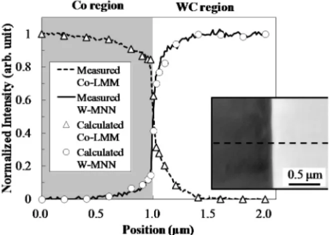
Figure 2 shows the line profiles of the W-MNN and
Co-LMM peaks obtained by the measurement (lines) and calculation (symbols) across the WC/Co interface of the model sample. It is found that the calculated distributions of the W-MNN and Co-LMM peak intensities were in good agreement with the measured distributions. For both the W-MNN profile and Co-LMM profile, the tails caused by the backscattering effect extend to about 500 nm. These results indicate that a model sample prepared by electrodeposition of metal elements on the flat grain surface is effective for experimentally studying the backscattering effect across the interface. It should be noted that although Auger electrons generated by cascade secondary electrons were ignored in the present calculation, the calculated results were in reasonable agreement with the measurement. This is attributed to the selection of the high-energy W-MNN and Co-LMM Auger peaks: The cascade secondary electrons have insufficient energy to ionize the W M and Co L shells, and thus have a negligible effect on the generation of W-MNN and Co-LMM Auger electrons.
3.2. Distribution of W near WC/Co interface in tungsten carbide tool sample
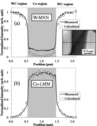
Figures 3(a) and (b) shows the measured and calculated W-MNN and Co-LMM line profiles across the WC/Co/WC interface of the tungsten carbide tool sample. The calculated W-MNN intensity decreases to almost zero at the middle of the Co region, which is approximately 500 nm from the WC/Co interface. In contrast, the measured profile shows nearly constant intensity of 0.18 within the Co region. Assuming that the intensity of the measured W-MNN profile within the Co region comes from the backscattering effect due to neighboring WC grains and from W atoms diffused into the Co region, the difference between the measured and calculated W-MNN profiles can be regarded as the net intensity of W-MNN derived from the W atoms diffused into the Co region. The assumption is of limited effectiveness in quantitative analysis using relative sensitivity factors (RSFs) because the quantification using RSFs is accurate for the homogeneous bulk sample surface and because parameters including the backscattering factor used in the calculation of AMRSFs depend on the position in the present system. Under the present assumption, the concentration of W in the Co region was estimated from the difference between calculated and measured
Fig. 2. Measured (lines) and calculated (symbols) line profiles of the W-MNN and Co-LMM peaks across the WC/Co interface of the model sample. The intensities are normalized by the maximum value of each profile. Inset shows the SEM image of the WC/Co model sample. The line profile was measured along the dashed line in the SEM image.
intensities at the middle of the Co region since the W-MNN intensity due to backscattered electrons is negligible at the middle of the Co region, as seen in the calculated profile in Fig. 3(b). In this way, we obtained a reasonable estimate of the W concentration by quantification using AMRSFs. The concentration of the W atoms diffused into the Co region, relative to Co in the Co region, was estimated to be 2.4 at%. According to the binary phase diagram of WC-Co [11], the degree of solubility of WC in Co is 15 at% at 1320°C, which is the freezing point of Co, and the solubility decreases toward a few atom percent with decreasing temperature, suggesting that the present results seem to be reasonable.
4. Summary
In this study, quantitative analysis of W diffused into the Co region in tungsten carbide tools was investigated through AES measurements and MC simulation. For this
purpose, a simple calculation model was used to calculate AES line profiles across the WC/C interface. To assess the proposed method, a model sample of the WC/Co interface with negligible diffusion of W was prepared. The results revealed that the method can provide a reasonable estimate of the concentration of W diffused into the Co region. Consequently, this approach was found to be effective for quantitative analysis of the diffusion of W in the Co region at 1 m from the WC/Co interface in tungsten carbide tools. A detailed investigation of relation between the amount of W diffused into Co region and the mechanical properties of tungsten carbide tools is underway and will be reported soon.
5. References
[1] H. Suzuki, M. Sugiyama, and T. Umeda, J. Japan Inst. Metals 29, 974 (1965).
[2] B. S. Park, Y. J. Baik, K. R. Lee, K. Y. Eun, and D. H. Kim, Diamond and related materials 2, 910 (1993). [3] R. Shimizu, M. Aratama, S. Ichimura, Y. Yamazaki,
and T. Ikuta, Appl. Phys. Lett. 31, 692 (1977). [4] J. S. Santos, R. Matos, F. Trivinho-Strixino, E. C.
Pereira, Electrochimica Acta 53 (2007) 644
[5] D. Drouin, A. R. Couture, D. Joly, X. Tastet, V. Aimez and R. Gauvin, SCANNING 29, 92 (2007).
[6] P. Hovington, D. Drouin, and R. Gauvin, SCANNING
19, 1 (1997).
[7] D. Drouin, P. Hovington, and R. Gauvin, SCANNING
19, 20 (1997).
[8] P. Hovington, D. Drouin, and R. Gauvin, D. C. Joy, N. Evans, SCANNING 19, 29 (1997).
[9] E. Casnati, A. Tartari, C. Baraldi, J. Phys. B 15, 155 (1982).
[10] K. Siegbahn, C. Nording, S. Karson, I. Lindgren, B. Lindgren, “ESCA, Atomic, Molecular and Solid State Structure Studied by Means of Electron Spectroscopy”, Almqvist and Wiksells (1967). [11] E. J. Sandford and E. M. Trent, Iron and Steel Inst.,
Spec. Rep. 38, 84 (1947).
Fig. 3. (a) W-MNN and (b) Co-LMM line profiles across the WC/Co/WC interface of the tungsten carbide tool sample. Solid lines and circles indicate the measured and calculated profiles. Intensities are normalized by the maximum value of each profile. Inset shows the SEM image of the surface of the tungsten carbide tool sample. The line profile was measured along the dashed line in the SEM image.
査読コメント 査読者1.永富 隆清(旭化成) MC シミュレーションを AES データ解析へ応用し た面白い検討であり,JSA 誌への掲載の価値がある と考えます. [査読者 1-1] 3.2 節 Co 領域への W 拡散による W-MNN 強度 実測値と計算値との差異について(初稿段階での議 論)
“This difference seems to be effective for qualitative analysis of W atoms in the Co region, including the WC/Co interface.” 意味が不明です.プロファイルの違いがなぜ“定 性分析に有効”なのでしょうか?「実験と計算の差 を定量」することが目的ではないのでしょうか? また,この段落の最後で Co 領域の中心付近の AMRSF を採用して濃度換算した結果を述べていま すが,結果が reasonable と結論されている論理が理 解できません.論理的な説明を加えてください.こ の点に関して,以下質問があります. 少なくとも実験プロファイルと計算プロファイル を比べたときに,モデルサンプルで実験結果を計算 で再現できた,と結論する場合,実サンプルでも計 算結果程度の後方散乱の影響が Co 領域に存在する ことになります.また,拡散したW の濃度は WC/Co 界面で最も高く,Co 領域の中心付近は低いのが一般 的だと考えます.そうすると,実験で得られたCo 中 の W プロファイルが界面であまりテールを引かず に Co 領域全体で一定に近いということは,著者ら が説明していない効果,すなわちWC/Co 界面の WC 領域でのW の欠乏の影響(Co 中の後方散乱効果が 低くなっている)が大きいことを示しています.い かがでしょうか? すなわち,Co 領域の中心付近での AMRSF を用い て求めることで,定量値が大きく向上しているか? という疑問にもつながります.これらも踏まえて回 答及び改定をご検討ください. [著者]
・“This difference seems to be effective for qualitative analysis of W atoms in the Co region, including the WC/Co interface.”の文章について 「プロファイルの違いが,これまで判断すらでき なかった元素の有無の判断に有効」という意味で記 載しておりまして,続く文章である,「界面近傍で定 量分析を行うにはAMRSF に含まれる背面散乱補正 係数を界面近傍用に修正しないと定量結果を過小評 価してしまう」という文章の前置きに使っておりま した.しかし,背景で元素の有無の判断の重要性に は明確に触れていないことから,本文中で必ずしも 触れる必要のある要素ではなく,文脈上前触れのな いものとなりますので不要と判断し,定性分析のく だりは削除いたしました.また同じ理由で 3.2 と
summary 中の qualitative and quantitative analysis とい う表現について qualitative を削除し,quantitative analysis という表現に変更いたしました. ・定量結果が reasonable であると述べる理由につい て WC-Co の二元系状態図から,WC の Co に対する 溶解度は最大でもCo 相の凝固点で 15 atom%程度で す.この値に対して 2.5 atom%という値は逸脱して おらず,reasonable と判断しております.その旨をよ り明確に記述いたします. ・W 欠乏の影響について 結果の吟味及びご指摘ありがとうございます.結 果に対する考察が深まりました.本研究における背 面散乱電子の影響の計算結果は WC 中に W が十分 に存在していることを仮定しているので,WC 粒子 中で W の欠乏が起きている系では適用限界を越え てしまい,定量精度の向上に繋がらないのではない か,ということでよろしいでしょうか. AES での Co 中 W のラインプロファイルは界面近 くまで平坦であり,これはご指摘の通り一般的な拡 散とは異なっており,『(1) WC 粒子中の W の欠乏』 か,または『(2)界面近傍での Co 中の W の減少』を 示唆していると思われます.これに関しまして,サ ンプルの液相焼結による生成過程に関連して(2)を 考えることで,(1)の WC 粒子中の W の欠乏を考え なくても説明可能と考えております. (1) WC 粒子中の W の欠乏 下記の理由から,可能性は低いと考えております. 文献を一通り確認しておりますが,界面近傍の WC 粒子中のW の減少(欠乏)を論じている文献は今の ところ存じ上げません.また,WC 中の W が欠乏し ていると仮定した場合,WC 粒子内の AES によるラ イン分析結果についてWC/Co 近傍から 200~300 nm の領域に渡って計算結果に対して実験値<計算値と なるような強度差が生じることが考えられますが, この領域では欠乏を判断できる程の強度差は生じて
いないように見えます. (2) 界面近傍での Co 中の W の減少 Co 中の W 濃度の分布が,一般的な拡散に見られ る分布とは異なり,実際に界面付近で減少している 可能性が考えられます.これについては焼結の過程 からWC-Co の二元系状態図[11]に基づいてご説明い たします. 一般にWC と Co の焼結は 1320℃より上の温度に おいて,WC が Co に対して溶解する条件で行われ ます(L+WC の状態).冷却開始段階(1320℃以上)では, WC と Co の混合された液相と,WC 固相が存在して い ま す(L+WC の 状 態 ) . 本 論 文 に お け る W の dissolved と diffused はこの段階でのことを指してお ります.冷却が進み,温度が1320℃に到達するまで, 溶解度の低下により液相中からWC 固相が新たに析 出し,さらにもともとあったWC 固相は成長します. 温度が1320℃を下回ると,液相中の Co が凝固しま す.(γ+WC の状態).WC の溶解度は 15 at%程度を 開始点として,室温に向かうに従い数 at%以下まで 低下します.この間でも溶解度が減少した分,WC の 成長が起こります.しかしこれは平衡状態の話であ り,実際には冷却速度にもよりますが Co 中に WC が過飽和の状態で存在しています. ここからは私の推測です.固体状態であるγ+WC 状態における冷却では,液相の存在したL+WC の状 態とは異なり,Co 中に溶解する WC の移動が限定 的であると仮定します.そうすると,溶解度低下に よるCo 中の WC の放出と,WC の受け取りによる WC 固相の成長が成立するのは WC/Co 界面付近の みであり,Co 相の中央部では WC が過飽和のまま 溶解して存在すると考えられます.その結果,Co 相 中の W の濃度分布は一般的な拡散に見られる分布 とはならず,界面近傍で減少し,中央付近で増加し たグラフになることが考えられます. 以上の(2)の考察を,ラインプロファイルに対する 考察として,本文中3.2 に追記いたしました.また, ラインプロファイル形状の理由を測定対象に依るも のとし,後方散乱の影響がモデルサンプルとそう変 わりないと仮定した考察を進めたことから,アブス トラクトの最後の文章についても,『後方散乱の効果 を考慮した...』としました. [査読者 1-2] (1-1 の回答後)ここまで議論するのであれば,WC のCo への固溶を考えているので,C-KLL のプロファ イルも含めた議論が必要では? [著者] 厳密には C-KLL のプロファイルや濃度に言及す べきと存じますが,本論文ではCo と W の相対値を もって定量値が妥当かどうかを議論したく存じます. 本文の記述は下記のようにしました.
The concentration of the W atoms diffused into the Co region, relative to Co in the Co region, was estimated to be 2.4 at%. [査読者 1-3] Co 領域で W の強度がフラットです.Co/WC 界面 に近い方が後方散乱電子によってWC 領域から発生 するW-MNN 電子が多いわけですから,W-MNN の プロファイルをそのまま理解すれば,Co 領域の中心 の方がW 拡散量が多い(濃度が高い)ことを意味し ます.すなわち逆にCo 濃度を考えると,Co 領域の 中心ほど Co 濃度が低く,界面付近の方が高い.そ れほど濃度差が無いにしても,こういう傾向が有る としたときに,このCo 領域での Co のプロファイル はreasonable なのでしょうか? [著者] 前回のご質問の趣旨を勘違いしていたようです. 申し訳ございません.ご指摘の Co の濃度傾向に加 えて,電子の散乱領域に占める Co 相の割合の変化 を考えれば,このプロファイル形状を説明できると 考えております.モデルサンプルのCo-KLL の実測 値(Fig. 2)を見ると,照射位置 0.5 μm~0.9 μm の間で, 界面に近づくにつれて強度が15%程度減少しており ます.これは界面に近づくにつれて入射電子の散乱 領域中に占める Co 相の割合が減少しているからで あると思われます.このことはFig. 3 の界面近傍で も同様に起きていると思われます.Fig. 3(b)で得られ る Co-KLL プロファイルは Co 濃度差による下に凸 のグラフと,散乱中の Co 相の占める割合の変化に よる上に凸のグラフの掛け算であり,その結果が, やや上に凸のプロファイルであると考えられます. [査読者 1-4] もう一点,質問したかったのは,WC/Co 領域での Co のテールです.WC 領域の方が Co 領域よりも一 次電子の広がりが狭い(あるいは同程度)と予想さ れるにも関わらず,WC 領域の Co のプロファイル の強度が,Co 領域の W の強度よりも随分高い.こ れに同期して,WC 中の W 強度も大分低い.左右ど ちらの Co/WC 界面も同様の鈍り方ですので,界面
が一次電子ビームに対して傾いているというよりも, WC の中へ Co が拡散していると考える方がリーズ ナブルでは? [著者] Co 中と WC 中における電子の侵入深さの差によ るものと考えております.モデルサンプルの系で説 明いたします.Fig. A に,20 keV の電子ビームを WC/Co に照射した際の電子の散乱の様子を示しま す.運動エネルギーが778 eV(Co L 殻のイオン化エ ネルギー)以下の電子はカットオフしています.WC 領域に照射された一次電子は Co 領域に照射された 場合と比べ縦に潰れた形となり,比較的浅い領域で 電子が散乱しています.そして WC/Co 界面を越境 した電子はWC 側に照射した場合の方が Co 側に照 射した場合よりも表面側に集まっているように見え ます. 具体的にはWC/Co 界面から 100 nm 以内の距離で は,WC 領域側から電子を入射して Co 領域の Co を 励起する場合の方が,Co 領域側から電子を入射して WC 領域の W を励起する場合の方よりも,一次電子 が表面に集中しており効率が良いということです. Fig. B に,表面から深さ 5 nm 以内の範囲における, WC 領域に電子を入射した際に Co 領域表面で起き る弾性散乱の数と,Co 領域に電子を入射した際に WC 領域表面で起きる弾性散乱の数の比較を示しま す.前者は Co L 殻のイオン化エネルギー以上の運 動エネルギーを持つ電子のみ,後者は W M 殻のイ オン化エネルギー以上の運動エネルギーを持つ電子 のみカウントしています.界面からの距離100 nm 以 内ではWC 領域に電子を入射させて Co の内殻励起 が起こる機会の方が,Co 領域の入射で W 内殻励起 が起こる機会よりも多いことが分かります. [査読者 1-5] 回答を拝見しました.補足で示していただいた データ(図A,B)の解釈に関して注意すべき点は, 電子軌道全体像に比べてずっと狭い極表面でしか オージェ電子が発生しないこと,弾性散乱の数と発 生するオージェ電子数は相関しますが,直接的では ないこと,だと思います.自分たちで作ったMC コー ドではないので欲しいデータをうまく抽出できませ んから,この部分の議論には限界がある(推定しか できない)と思います. 査読者2.堤 健一(日本電子) 本論文はオージェ電子分光法の横方向の空間分解 能を議論する上で重要となる,背面散乱電子による 分析領域の拡大量を,実測定の結果とモンテカルロ シミュレーションの結果を照らし合わせて,定量的 に検証したことと,焼結された WC 工具の中で Co 結晶粒中に W 原子が拡散する現象を捉えた論文で あるため,掲載する価値は非常に高いと考えます. [査読者 2-1] しかし,この論文中で核となっている実測された オージェスペクトルが示されておらず,ラインプロ Fig. A WC/Co モデルサンプルに電子を入射したとき の電子散乱の様子.入射位置はそれぞれ,(a)界面から 100 nm 離れた Co 領域側, (b)WC/Co 界面上,(c)界面 から100 nm 離れた WC 領域側. Fig. B WC 領域に電子を入射した際に Co 領域表面で 発生する弾性散乱の数と、Co 領域に電子を入射した際 にWC 領域表面で発生する弾性散乱の数 0 1000 2000 3000 4000 5000 6000 7000 0 200 400 600 弾性散乱 の 数 入射位置から界面までの距離(nm) WC領域の電子(Co領域に入射) Co領域の電子(WC領域に入射)
ファイルの記述でも,オージェスペクトルのどの点 (エネルギー値)をピークとし,どの点(エネルギー値) をバックグラウンドに指定してラインプロファイル を形成したのか,または別にバックグラウンド曲線 を定義して差し引いたのかを,明確に記述していな いため,他者が追試することを考えると,少し不親 切に思われます.ご検討をお願いします. [著者] 本試験では微分スペクトルのPeak-to-Peak による ピーク強度の導出を行っております.また,W-MNN とCo-LMM のピーク値は 1738 eV および 778 eV を 採用しています. [査読者 2-2] 他者が追試するという観点で見た場合に,
Cross-section Polisher と FIB の断面作製条件(加速電圧や電
流など)を記載するのが親切かと思いますが,いかが
でしょうか.ご検討ください. [著者]
Cross-section Polisher と FIB の断面作成条件を記載 いたしました.