PAPER
Parallelization of Boost and Buck Type DC-DC Converters by Individual Passivity-Based Control
Yuma MURAKAWA†a),Student Member, Yuhei SADANDA†b),Nonmember,andTakashi HIKIHARA†c),Fellow
SUMMARY This paper discusses the parallelization of boost and buck converters. Passivity-based control is applied to each converter to achieve the asymptotic stability of the system. The ripple characteristics, error char- acteristics, and time constants of the parallelized converters are discussed with considering the dependency on the feedback gains. The numerical re- sults are confirmed to coincide with the results in the experiment for certain feedback gains. The stability of the system is also discussed in simulation and experiment. The results will be a step to achieve the design of parallel converters.
key words: parallelization, DC-DC converter, passivity-based control, distributed power source
1. Introduction
In recent years, distributed power sources, such as solar cells and batteries, have actively been studied[1],[2]. It is tightly related to the global demand for clean energy. These sources tend to have a relatively small and limited amount of output. Cooperative use of various power sources may realize distributed generation[3],[4]. Power converters play a very important role as interfaces for them.
The parallelization of power converters has widely been discussed for the past two decades [5]. There have been works that focus on obtaining a larger power capacity by shar- ing the load current equally between parallelized converters.
However, the parallel connection of different converters nor obtaining uneven current distribution has not been a subject of study. The multiple-input DC-DC converter is consid- ered in[6] for the combination of various power sources.
The generalized argument of such a system has not been accomplished though.
The connection of different power sources and convert- ers will make the system complexed. The control method based on the knowledge of the whole system is unrealistic.
Decentralized control and design are necessary for the scala- bility and diversity of the system. Therefore, passivity-based control (PBC) is proposed[7]. The control method keeps the advantage of the passive characteristics which inherently physical systems have. It aims to stabilize the system by modifying the energy function. The application of PBC to DC-DC converters was given in[8]. More generalized
Manuscript received May 13, 2019.
Manuscript revised October 24, 2019.
†The authors are with the Department of Electrical Engineering, Kyoto University, Kyoto-shi, 615-8510 Japan.
a) E-mail: [email protected] b) E-mail: [email protected] c) E-mail: [email protected]
DOI: 10.1587/transfun.2019EAP1069
Fig. 1 Schematic circuit of parallelized boost and buck converters.
arguments were well explained in[9],[10].
An electric circuit composed of passive elements is known to be passive[11]. Hence, by applying PBC to the converters individually and assuring each energy function to be asymptotically stable, it is expected that the parallelized system will also be asymptotically stable. From this per- spective, the stabilization of ´Cuk converters connected in parallel by PBC is discussed in [12]. The application of PBC is extended to ring coupled boost converters[13].
This paper focuses on parallelizing two different types of DC-DC converters; boost and buck. They are one of the most major converters which are used in many types of electrical equipment. Boost and buck converters have the function of stepping the voltage up and down, respectively.
Therefore, the parallelization of these converters enables the combination of a wide variety of power sources with various output voltages. Here, PBC is introduced to each converter individually. Their characteristics are explored numerically and experimentally. In Sect. 2, we will analytically show that the individual PBC assures the whole parallelized system to be asymptotically stable. Sections 3 and 4 are devoted to the numerical and experimental confirmation, respectively.
Section 5 is the conclusion.
2. Parallelization of Boost and Buck Converters and Application of Passivity-Based Control
Figure 1 is a schematic circuit of parallelized boost and buck converters. The converters are sharing a load at the output. Each converter consists of voltage sourceE, loadR, inductanceL, capacitanceC, switchu, and diodeD. Here, i denotes the inductor current andv the capacitor voltage.
Copyright © 2020 The Institute of Electronics, Information and Communication Engineers
The subscripts ‘1’ and ‘2’ correspond to converter #1 (boost converter) and converter #2 (buck converter), respectively.
Note that all circuit elements mentioned in this section are ideal.
2.1 System Model
The Kirchhoff’s laws give the differential equations of the parallelized circuit shown in Fig. 1 as
L1˙i1 =−(1−u1)v+E1, L2˙i2 =−v+u2E2, C12v˙ =(1−u1)i1+i2− v
R,
(1)
whereC12=C1+C2. The dot (˙) on the variable is a notation for time differentiation. The system is discontinuous with the switching variablesu1,u2 ∈ {0,1}, switching the system structure. Regulation of power converters implies switching operation, which corresponds to the switching variablesu1 andu2.
Assuming a high frequency switched pulse width mod- ulation (PWM), the state averaging model of DC-DC con- verters is obtained[8],[14]. By averaging Eq. (1), we obtain
L1˙i1 =−(1−µ1)v+E1, L2˙i2 =−v+µ2E2, C12v˙ =(1−µ1)i1+i2− v
R.
(2)
The switching variablesu1,u2are replaced with duty ratios µ1, µ2 ∈[0,1].
Control objective, here, would be obtaining the asymp- totical stability at the desired state [i1,i2, v]=[i1d,i2d, vd], by modifying the duty ratiosµ1andµ2. Null curve of Eq. (2) is obtained as
µ1 =1−E1 v , µ2 = v
E2,
E1i1+µ2E2i2 =v2 R.
(3)
The desired state [i1i2v] = [i1di2dvd] must be chosen to satisfy Eq. (3). The steady state implies that all input energy is consumed at the load, and a specific duty ratio will be chosen for a specific output voltage. Thus the desired duty ratios become
µ1d=1−E1 vd, µ2d= vd
E2, (4)
which correspond to the desired output ordervd.
2.2 Application of Passivity-Based Control
Viewing the parallelized system as a whole, it may adopt sev- eral control schemes, for example, approximate linearization and state feedback. However, such an approach is the lack of scalability; the capability of parallelizing more converters.
It is natural that decentralized control technique is adopted to focus on each converter. PBC is applied to each converter to assure the stability of the parallelized system.
PBC for each converter are given by
µ1=µ1d−k1(vdi1−vi1d) (k1>0),
µ2=µ2d−k2(i2−i2d) (k2>0), (5) whose derivation is defined in the appendix. The shaped storage functions for each converter are
H1(i1, v)=1
2L1(i1−i1d)2+1
2C1(v−vd)2, H2(i2, v)=1
2L2(i2−i2d)2+1
2C2(v−vd)2. (6) Then, the storage functionH12for the whole system is their summation
H12(i1,i2, v)=H1(i1, v)+H2(i2, v)
= 1
2L1(i1−i1d)2+1
2L2(i2−i2d)2+1
2C12(v−vd)2. (7) The stability of the desired state [i1i2v] = [i1di2dvd] is theoretically examined by the Lyapunov stability theory [15]. Differentiating the desired storage function gives
dH12 dt =∂H12
∂i1 di1
dt +∂H12
∂i2 di2
dt +∂H12
∂v dv dt
=(µ1−µ1d) (vdi1−vi1d)+(µ2−µ2d)E(i2−i2d)
−(v−vd)2
R . (8)
With the control law Eq. (5), we obtain dH12
dt =−k1(vdi1−vi1d)2−k2E(i2−i2d)2− (v−vd)2
R , (9)
which shows that H12 decreases monotonically. There- fore, the desired storage function H12 can be a candidate of Lyapunov function for the parallelized system described as Eq. (2) with the control law Eq. (5). It ensures the asym- totic stability around [i1i2v]=[i1di2dvd].
We have shown that individual application of PBC to each converter can also stabilize the parallelized system.
This is due to the passivity of the whole system. Note that the discussion owes to the ideal setting of circuit elements.
Hence, we must take the nonideality into account when we apply these control laws to the practical converters.
3. Numerical Simulation
In this section, we will examine the characteristics of the parallelized system with PBC. The result focuses on the dependence on control gainsk1andk2, which govern both the steady state and the transient of the system.
3.1 Setups of Simulation
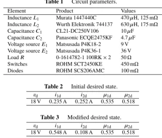
In the simulation, the circuit is modeled using MAT- LAB/SIMULINK. Here, we introduce the parameters of cir- cuit elements listed in Table 1. Those resistances are all parasitic resistances except for the loadRand are considered to be connected in series to each element. They correspond to the elements in the experiments.
In the simulation, the duty ratios of each converter,µ1 and µ2, are estimated by Eq. (5). The switches are also nonideal having a discrete on and off states, so we must have an A/D conversion method maintaining the calculated on and off ratio. PWM is widely used due to its simplicity and easy implementation. However, according to the increase of switching frequency, it must require a significantly fast clock speed of the controller to maintain its resolution of the pulse width. Therefore, we adopt a pulse density modulation, from the expectation of increased switching speed. One of the modulations is∆Σmodulation. Substituting∆Σmodulation, the averaged characteristics of DC-DC converters is kept at sufficiently large frequency[16]. In the following simulation, the pulse width is fixed at 1µs for both converters.
With the aforementioned circuit and controller settings, we consider the supplied power adjustment. While the de- sired output voltage stays unchanged, the desired input cur- rent of each converter is modified. The target is set initially as shown in Table 2. At the instancet =0, we will give a step like change to the target to be shown in Table 3, which is chosen not to alter the power consumption of the whole system.
The elements we have used in the simulation are non- ideal, which makes it difficult for us to obtain the exact values of the steady state. Here, we have considered exclusively the diode’s voltage dropvon(=1.35 V)and its power consump- tion. Hence, the target depends on the relationship
µ1d=1− E1 vd+von, µ2d= vd+von
E2+von, E1i1d+µ2dE2i2d= vd2
R +(1−µ1d)voni1d +(1−µ2d)voni2d.
(10)
However, they do not exactly describe the steady state, be- cause the inner resistances are out of consideration. There- fore, the steady state errors remain. In particular, the desired state with an extremely high boost ratio leads to the signif- icant errors due to the inner resistances with large power
Table 1 Circuit parameters.
Element Product Values
InductanceL1 Murata 1447440C 470µH, 125 mΩ InductanceL2 Wurth Elektronik 744137 630µH, 175 mΩ CapacitanceC1 CL21-DC250V106 10µF CapacitanceC2 Panasonic ECQE2475KF 4.7µF Voltage sourceE1 Matsusada P4K18-2 9 V Voltage sourceE2 Matsusada P4K36-1 36 V LoadR 0-1614782-1 100RK×2 50Ω
Switches ROHM SCT2450KE 450 mΩ
Diodes ROHM SCS206AMC 100 mΩ
Table 2 Initial desired state.
vd i1d i2d µ1d µ2d
18 V 0.235 A 0.252 A 0.535 0.518
Table 3 Modified desired state.
vd i1d i2d µ1d µ2d
18 V 0.548 A 0.108 A 0.535 0.518
consumption. In this case, the error cannot be compensated by the feedback control. So that the decision of the de- sired state is restricted to have sufficiently low inner power consumption.
3.2 Simulational Results
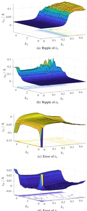
The steady state characteristics are shown in Figs. 2 and 3.
Here, the steady state ripple and the errors of input currents and output voltage are evaluated. Subscripts ‘r’ and ‘e’ stand for ripple and error, respectively.
In Figs. 2(a) and 2(b), there appear large ripples when gains are set higher than a certain threshold. It is caused by high gain settings which makes the ripple to be fed un- necessarily to the feedback controller. Also, in Fig. 2(a), the contours are almost parallel tok2axis. It means that the rip- ple ofi1is independent ofk2. A similar feature can be seen in Fig. 2(b). The ripple ofi2is independent onk1. Each gain setting should be set less than its threshold in order to avoid large ripples. The thresholds can be obtained individually because the ripple characteristics were independent.
Figures 2(c) and 2(d) show the error function depend- ing on gains. It is shown that the errors become significantly large at small gain region in which the effect of feedback control is exceedingly reduced. The error can be sufficiently restricted by one of the gains. This is due to the load shar- ing between the converters. The gains, set larger than the thresholds, cannot keep the error lower due to the saturation of duty ratios or large ripples. The above discussions insist that the gains are limited in a range for appropriate steady state operation.
In Fig. 3, steady state characteristics of the output volt- age are shown. Fig. 3(a) is similar to Fig. 2(a). The threshold seen in both figures has almost no difference. It is because the boost converter is more sensitive to output noise than the buck converter. Fig. 3(b) shows a flat surface in the center.
This portion corresponds to the appropriate gain settings seen in Fig. 2. It is confirmed that ripple and error characteristics of output voltage and input currents are related.
Fig. 2 Steady state current characteristics with regards tok1andk2.
Figure 4 shows the time constantτof the system. Here, τ is defined as the estimated duration ofH12to be 1/e of initial value. In the figure, the larger gains are set, the smaller τappears. However, it saturates due to the limit of duty ratio from 0 to 1.
In Fig. 4, the contours are almost parallel to one of the axes. It implies that the time constant of converters is in- dependent of each other. The time constant of the whole system is governed by the slower of the two. These charac- teristics assure the extension of parallelization into multiple converters.
Fig. 3 Steady state voltage characteristics with regards tok1andk2.
Fig. 4 Surface of time constantτwith regards tok1andk2.
Figure 5 shows the transient waveforms ofi1andi2for some couples ofk1andk2. In Fig. 5(a), it is shown that time for the convergence ofi1 is almost independent of k2. It corresponds to the results in Fig. 4. The same feature can be seen in Fig. 5(b). In addition, it is confirmed that large gain settings lead to significantly large ripples.
In summary, we have discussed the characteristics of the parallelized system governed by the gainsk1andk2. The simulation concludes that both the steady state and transient characteristics of paralleled converters keep independent.
Also, it is shown that there is a region of gains for a valid converter operation. This knowledge is applied to the design of paralleled converter systems. In the next section, the parameter in the region will be examined in experiments.
Note that these results are obtained for a fixed circuit parameter and the desired state. The region of the feedback gains for a valid converter operation definitely depends on the circuit parameters and the desired states. Though they are not examined here, it is expected that they might have a region for achieving similar results. From the numerical results and discussions in this section, it is anticipated that the region
Fig. 5 Transient characteristics of currents.
of the circuit parameters and the desired states would have a relationship particularly to internal power consumption and output capacitance.
4. Experimental System and Results
In this section, the experimental results of the parallelized system are shown. Supplied power is adjusted corresponding to the simulation. The target states are adopted as shown in Tables 2 and 3.
4.1 Settings of Experiment
Figure 6 shows the photo of experimental system. The paral- lel system with boost and buck converters are implemented with elements shown in Table 1. Here, current sensors are adopted to measure inductor currents of converters. They are Analog Devices LTC6102 for the boost converter and LEM LTS6-NP for the buck converter. The measured cur- rents are applied for feedback control. Furthermore, the main switches of the converters are driven by the gate driver Silicon Labs SI823BB.
In the experiment, myRIO FPGA is used as the con- troller to calculate the duty ratio and to generate the switch- ing signal. The duty ratio is calculated according to Eq. (5).
The feedback gains are set atk1 = 0.03 andk2 = 1. The switching signal is generated based on the duty ratio by∆Σ modulation, which is applied to the gate driver.
4.2 Experimental Results
Both the experimental and simulational results are shown in Fig. 7. In the figure,i1,i2, andvare shown as the waveforms
Fig. 6 Photo of the experimental system.
Fig. 7 Experimental and simulation result of a parallelized system.
obtained in the experiment. The subscription ‘sim’ and ‘exp’
stand for simulation and experiment, respectively.
At the steady state, it is shown that the experimental system becomes stable. The results well coincide with the simulation after the adjustment of input power. Currenti1 shows a larger error at steady state. It is found to be caused by the parasitic resistances and low gain setting.
At the transient, the experimentally obtainedi1 shows overshoots in waveforms, which are not observed in the cor- responding simulation. This is due to the sensor characteris- tics. The quick response time or the low-pass characteristics of the sensor may possibly cause overshoots or even insta- bility with large gain settings. The low gain setting was appropriate. In order to avoid this conflict, a sufficiently quick response is requested to the sensors.
On the other hand, buck converter currenti2 showed the good coincidence of simulation and experimental results.
This clearly shows the independent characteristics, in that the overshoot ofi1did not affect the transient ofi2. The experi- mental result also showed that their transient waveforms are governed by their individual time constant.
The simulation and experimental results of output volt- age v also well coincide. During the transient, v almost shows no fluctuation from the steady state, due to sufficient
output capacitance. Therefore, the interaction among the converters is reduced since the interconnection between the converters is limited. The independency of the converters are achieved from the circuit parameters as well as control technique.
5. Conclusion
Parallelization of boost and buck converter and their PBC were examined numerically and experimentally. Individ- ual application of PBC to the boost and buck converters achieved asymptotical stabilization of the parallelized sys- tem. Through numerical simulation, the dependence on the feedback gains was investigated in terms of ripple charac- teristics, error characteristics, and time constant. It was concluded that the gain settings were found for steady state operation. It was also confirmed that each converter had in- dependent characteristics. Stability and independent charac- teristics were also confirmed through the experiment. These results enable the design for more diverse parallelization of converters.
Acknowledgments
This work was partially supported by the Super Cluster Pro- gram from Japan Science and Technology Agency. The authors would like to thank Dr. Takafumi Okuda for his support in the experiment. The author, YM, acknowledges Mr. Manuel Sanchez for his support in programming myRIO FPGA.
References
[1] N. Kannan and D. Vakeesan, “Solar energy for future world: - A re- view,” Renewable and Sustainable Energy Reviews, vol.62, pp.1092–
1105, 2016.
[2] J.B. Goodenough and K.S. Park, “The Li-ion rechargeable battery:
A perspective,” J. Am. Chem. Soc., vol.135, no.4, pp.1167–1176, 2013.
[3] T. Ackermann, G. Andersson, and L. Söder, “Distributed generation:
A definition,” Electr. Pow. Syst. Res., vol.57, no.3, pp.195–204, 2001.
[4] G. Pepermans, J. Driesen, D. Haeseldonckx, R. Belmans, and W. D’haeseleer, “Distributed generation: Definition, benefits and issues,” Energ. Policy, vol.33, no.6, pp.787–798, 2005.
[5] Y. Huang and C.K. Tse, “Circuit theoretic classification of paral- lel connected dc-dc converters,” IEEE Trans. Circuits Syst. I, Reg.
Papers, vol.54, no.5, no.5, pp.1099–1108, 2007.
[6] H. Matsuo, F. Kurokawa, T. Shigemizu, and N. Watanabe, “Char- acteristics of the multiple-input dc-dc converter,” IEEE Trans. Ind.
Electron., vol.51, no.3, pp.625–631, June 2004.
[7] R. Ortega, A.J. Van Der Schaft, I. Mareels, and B. Maschke, “Putting energy back in control,” IEEE Control Syst. Mag., vol.21, no.2, pp.18–33, April 2001.
[8] H. Sira-Ramirez, R. Perez-Moreno, R. Ortega, and M. Garcia- Esteban, “Passivity-based controllers for the stabilization of dc-to-dc power converters,” Automatica, vol.33, no.4, pp.499–513, 1997.
[9] R. Ortega, J. Perez, P. Nicklasson, and H. Sira-Ramirez, Passivity- based Control of Euler-Lagrange Systems: Mechanical, Electrical and Electromechanical Applications, Communications and Control Engineering, Springer-Verlag, 1998.
[10] H. Sira-Ramirez and R. Silva-Ortigoza, Control Design Techniques
in Power Electronics Devices, 2006 ed., Springer-Verlag, 2006.
[11] C. Desoer and E. Kuh, Basic Circuit Theory, McGraw Hill in- ternational editions: Electrical and electronic engineering series, McGraw-Hill, 1969.
[12] T. Hikihara and Y. Murakami, “Regulation of parallel converters with respect to stored energy and passivity characteristics,” IEICE Trans.
Fundamentals, vol.E94-A, no.3, pp.1010–1014, March 2011.
[13] R. Manohar and T. Hikihara, “Dynamic behaviour of a ring cou- pled boost converter system with passivity-based control,” CoRR, vol.abs/1810.00417, 2018.
[14] G. Escobar, A.J. Van der Schaft, and R. Ortega, “A Hamiltonian view- point in the modeling of switching power converters,” Automatica, vol.35, no.3, pp.445–452, 1999.
[15] A. Isidori, Nonlinear Control Systems, 3rd ed., Springer-Verlag, Berlin, Heidelberg, 1995.
[16] S.K. Dunlap and T.S. Fiez, “A noise-shaped switching power supply using a delta-sigma modulator,” IEEE Trans. Circuits Syst. I, Reg.
Papers, vol.51, no.6, pp.1051–1061, 2004.
Appendix: Derivation of Control Laws
State averaging model and definition of the shaped energy function will follow the works[8]–[10],[14].
A.1 Boost Converter
Consider a boost converter circuit shown in Fig. A·1, which has a function of stepping up the voltage at the output. The differential equations describing the circuit are
L1i˙1=−(1−µ1)v+E1, C1v˙=(1−µ1)i1− v
R, (A·1)
where stateu1 ∈ {0,1} is already replaced with duty ratio µ1∈[0,1].
The desired state [i1v] = [i1dvd] and corresponding desired duty ratioµ1=µ1dhave to satisfy
µ1=1−E1 v , E1i1= v2
R,
(A·2)
which are obtained by setting the left hand side of Eq. (A·1) to zero.
Desired storage function of the boost converter is de- fined as
H1(i1, v)= 1
2L1(i1−i1d)2+1
2C(v−vd)2, (A·3) which is shaped to have a minimum at the desired state. By differentiating this storage functionH1 along the trajectory of the boost converter described as Eq. (A·1), we obtain
dH1 dt =∂H1
∂i1 di1
dt +∂H1
∂v dv dt
=− (v−vd)2
R +(µ1−µ1d) (vdi1−vi1d). (A·4)
Fig. A·1 Boost converter.
Fig. A·2 Buck converter.
The first term of the right side stands for the dissipation and the second for the supplied power. Eq. (A·4) indicates that the boost converter system is a passive system with respect to the shaped storage functionH1, regardless ofµ1.
Regulating the supplied power to be minus ensures the convergence ofH1at the minimum value zero. Such regu- lation will be attained by the control law
µ1=µ1d−k1(vdi1−vi1d) (k1>0), (A·5) where k1 is a positive constant. By applying Eq. (A·5), H1<0 at [i1v],[i1dvd] is guaranteed. The desired storage function H1 becomes a Lyapunov function for the boost converter system. Therefore, asymptotic stability around [i1v]=[i1dvd] is achieved. Here, the constant valuek1is a feedback gain.
A.2 Buck Converter
Consider a buck converter circuit shown in Fig. A·2. Com- pared to a boost converter, it has the same elements but has a different topology making it have a different function of stepping the voltage down at the output.
The differential equations describing the buck converter are
L2˙i2 =−v+µ2E2, C2v˙=i2− v
R, (A·6)
where averaging has already taken place.
By setting the differential terms to zero, the steady state equation will be
µ2 = v
E2, i2 = v
R. (A·7)
The desired state [i2v]=[i2dvd] and the desired duty ratio µ2 =µ2dhave to be determined to satisfy Eq. (A·7).
The desired storage function is defined as H2(i2, v)=1
2L(i2−i2d)2+1
2C2(v−vd)2, (A·8)
which is shaped to have a minimum value zero at the desired state. Differentiating this storage functionH2along the tra- jectory of the buck converter system described as Eq. (A·6) gives
dH2 dt =∂H2
∂i2 di2
dt +∂H2
∂v dv dt
=− (v−vd)2
R +(µ2−µ2d)E2(i2−i2d). (A·9) The buck converter is shown to be a passive system with respect to a shaped storage functionH2. Here, applying the control law
µ2=µ2d−k2(i2−i2d) (k2>0), (A·10) ensuresH2 < 0 at [i2v],[i2dvd]. Hence,H2 becomes a Lyapunov function, which guarantees the asymptotic stabil- ity around [i2v]=[i2dvd].
Yuma Murakawa received his B.S. degrees in Electrical Engineering from Kyoto University, Japan in 2018. He is currently a graduate stu- dent at the Department of Electrical Engineering, Kyoto University. His research interests include power conversion and control.
Yuhei Sadanda received the B.S. and M.S.
degrees in Electrical Engineering from Kyoto University in 2015 and 2017, respectively. He is now with Kawasaki Heavy Industries, Ltd.
Takashi Hikihara received PhD from Kyoto University on 1990. Since 1997 he has been a faculty of Department of Electrical Engineering at Kyoto University, where he is currently a Pro- fessor. He is also Director General of Kyoto University Library Network. His research inter- ests are including nonlinear science, engineering applications of nonlinear dynamics, power elec- tronics, and sensor network. He is a member of the IEEE, APS, SIAM, ISICE, and IEE, Japan.