Design and implementation of Electrical Double Layer Capacitor (EDLC) Based 1U CubeSat Electrical Power System (EPS).
11
0
0
全文
(2)
(3)
(4)
(5)
(6)
(7)
(8)
(9)
(10)
(11)
図
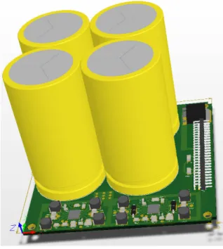
![Fig. 11 The EDLC used in our study [11]](https://thumb-ap.123doks.com/thumbv2/123deta/6807599.2230306/5.892.469.777.554.888/fig-edlc-used-study.webp)
+6
![Fig. 16 LTC3425 Boost converter chip [15]](https://thumb-ap.123doks.com/thumbv2/123deta/6807599.2230306/6.892.471.784.599.781/fig-ltc-boost-converter-chip.webp)
関連したドキュメント