SUMMARY Gallium nitride high electron mobility transistors (GaN HEMTs) were developed for millimeter-wave high power amplifier appli- cations. The device with a gate length of 80 nm and an InAlN barrier layer exhibited high drain current of more than 1.2 A/mm and high breakdown voltage of 73 V. A cut-offfrequency fTof 113 GHz and maximum oscilla- tion frequency fmaxof 230 GHz were achieved. The output power density reached 1 W/mm with a linear gain of 6.4 dB at load-pull measurements at 90 GHz. And we extracted equivalent circuit model parameters of the millimeter-wave InAlN/GaN HEMT and showed that the model was useful in simulating the millimeter-wave power performance. Also, we report a preliminary constant bias stress test result.
key words: GaN HEMT, Millimeter-wave, Power amplifier, Device model- ing
1. Introduction
With the spread of cellular and smart phones, higher ca- pacity in mobile backhaul and wireless access networks would be required despite microwave frequency bands get- ting highly congested. It is becoming difficult to find avail- able microwave frequency spectrum. Thus, millimeter-wave is expected to be an attractive frequency resource where wide bandwidth can be secured for high speed wireless communications. For example, the 70/80 GHz frequency band called E-band has attracted much attention as a multi- Gigabit capacity transport means in future networks due to its wide band spectrum of 5 GHz and a low cost of frequency licensing [1]. Some issues in promoting the millimeter- wave use are insufficient performance and high cost of the millimeter-wave devices. Especially, it is difficult to get a high output power amplifier with broad bandwidth.
GaN HEMT has attracted much attention as a device of millimeter-wave power amplifiers because of its sev- eral merits such as high breakdown voltage and high drain current due to high sheet carrier density of 2 dimensional electron gas (2DEG) of more than 1×1013cm−2. And Al- GaN/GaN HEMTs have been developed and used as mi- crowave power amplifiers of cellular base stations due to their high output power and high efficiency performance [2].
Recently, device scaling of GaN HEMTs has been in- tensively pursued while focusing on their millimeter-wave operation and the gate electrode is expected to shrink to sub-0.1µm [3]–[7]. There are, however, some problems in
Manuscript received July 14, 2014.
†The authors are with Fujitsu Limited and Fujitsu Laboratories Ltd., 10-1 Morinosato-Wakamiya, Atsugi, 243-0197 Japan.
a) E-mail: [email protected] DOI: 10.1587/transele.E97.C.923
shrinking the device. One is a short-channel effect such as drain induced barrier lowering, low output resistance, and poor pinched-offcharacteristics. To suppress the short- channel effect, the barrier layer between the gate electrode and an electron transit channel should be thinned for shrink- ing the gate length. A thinner AlGaN barrier layer, how- ever, leads to lower 2DEG density and lower output power, and diminishes the merits of GaN HEMTs [8], [9]. There- fore, larger band gap materials with lager polarization effect such as InAlN have been considered for use as the barrier layer for millimeter-wave operations [10], [11]. InAlN/GaN HEMT has a twice higher 2DEG density than AlGaN/GaN HEMT due to its larger conduction band discontinuity∆Ec and stronger spontaneous polarization effect [12], [13].
In a short-channel device, a buffer leakage current should also be considered to suppress the poor pinched-off characteristics. Thus, we studied a back barrier layer ef- fect on InAlN/GaN HEMTs with an AlGaN back barrier layer and an InGaN back barrier layer [14]–[16] in conjunc- tion with the charge trapping phenomenon. The polarization charges at upper and lower heterojunction interfaces of the InGaN back barrier layer cause high electric field, confining 2DEG to the channel layer. The InGaN back barrier layer suppresses the short-channel effect and enhances the output resistance.
The developed InAlN/GaN HEMT with a gate length of 80 nm exhibited a high drain current and high break- down voltage of higher than 70 V. A cut-offfrequency fT
of 113 GHz and maximum oscillation frequency fmax of 230 GHz were achieved.
In this paper, we describe the device structure and fabrication process of InAlN/GaN HEMTs and their DC and high frequency performance. Secondly, we explain an equivalent circuit model of InAlN/GaN HEMT, where we employ the Angelov GaN HEMT model. Its model parameters were extracted from the measured I-V and S- parameters, and the model simulation results were com- pared with power measurement results at 90 GHz. Finally, we report a preliminary constant bias stress test result.
2. InAlN/GaN HEMT Structure and Performance
2.1 Device Structure and Fabrication Process
Figure 1 shows our InAlN/GaN HEMT structure. Epitax- ial layers of an InAlN barrier layer, an AlN spacer layer, Copyright c⃝2014 The Institute of Electronics, Information and Communication Engineers
Fig. 1 InAlN/GaN HEMT structure with Y-shaped gate electrode.
a GaN channel layer, and a buffer layer were grown on a semi-insulated SiC substrate by the metal-organic chemi- cal vapor deposition (MOCVD) technique. The Al mole fraction was 17% so that the lattice constant of the InAlN matched with GaN. The thickness was as less as 6.6 nm and the AlN was 1.3 nm. The device fabrication process was as follows. Firstly, the device isolation region was formed by ion-implantation. To achieve a millimeter-wave operation, source and drain ohmic electrodes must have a low contact resistance. Since a large band gap of InAlN makes it difficult to get a good ohmic contact, the InAlN layer was partially removed by dry-etching. Then, the ohmic metal layers were evaporated and annealed at 600◦C. The ohmic contact resis- tance was around 0.8 Ω·mm. A SiN dielectric film was deposited by plasma-enhanced chemical vapor deposition (PECVD). The gate footprints were defined by the electron- beam lithography and the SiN film was dry-etched. Gate metals of Ni/Au were evaporated and lifted-off. To reduce the gate resistance, a Y-shaped gate structure was formed us- ing three photo resist layers. Fabricated GaN HEMTs have a gate width of 2×50µm, a gate-source distance of 0.75µm, and a gate-drain distance Lgd of 2µm.
2.2 InGaN Back Barrier
To suppress the short-channel effect, we studied a thin GaN channel layer of 50 nm on the back barrier layer. Since the current collapse problem may occur due to electron traps in the barrier layer and the buffer layer just under the chan- nel layer, we studied two kinds of barrier layers. One was an AlGaN barrier layer and the other was an InGaN barrier layer. Figure 2 shows the curve tracer ID–VD characteris- tics of fabricated InAlN/GaN HEMTs with an InGaN back barrier layer (right) and an AlGaN back barrier layer (left).
Drain voltages were applied up to 10 V and 20 V to check the current collapse. The gate length was 0.12 µm. The maximum gate voltage was 2 V by step of 0.5 V. The AlGaN back barrier HEMT caused a large current collapse as com- pared to the InGaN back barrier HEMT. We think that the electron traps in the AlGaN back layer or interfaces could have caused this current collapse.
Fig. 2 Curve tracer ID–VDcharacteristics of InAlN/GaN HEMTs with an InGaN back barrier layer (right) and an AlGaN back barrier layer (left).
Drain voltages were applied up to 10 V and 20 V to check the current col- lapse. Gate length is 0.12µm. GaN channel thickness is 50 nm.
Fig. 3 Breakdown characteristics of 80 nm GaN HEMT.
2.3 DC Performance
The DC and RF performance of the fabricated InAlN/GaN HEMT was estimated with a semiconductor parameter an- alyzer and a vector-network analyzer. As shown in Fig. 2 of drain current-voltage characteristics, the maximum drain current was higher than 1.6 A/mm at VGSof 2 V. There is a trade-offrelationship between high frequency performance and breakdown voltage. A larger gate-drain distance Lgd leads to a higher breakdown voltage although the high fre- quency gain decreases. We optimized the Lgd to 2µm with a breakdown voltage of 73 V (Fig. 3).
2.4 High Frequency Performance
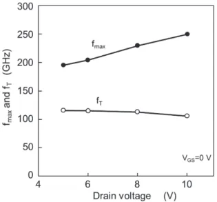
The high frequency performance of current gain cutofffre- quency fT and maximum oscillation frequency fmaxwas es- timated by measured S-parameters. Figure 4 shows drain- source voltage dependence of fT and fmax. It was observed that fT was 113 GHz with fmax of 230 GHz at a drain volt- age of 8 V. fmaxenhanced as drain voltage increased due to a decrease of output capacitance and an increase of output re- sistance. At a drain voltage of 10 V, fmaxreached 250 GHz.
An fTof more than 100 GHz was achieved at this drain volt- age range and gate voltage of 0 V.
We estimated the millimeter-wave power performance of the fabricated GaN HEMT at 90 GHz with a load-pull measurement system of Focus Microwave Inc. and wafer
Fig. 4 Drain-source voltage dependence of fmaxand fTestimated by S- parameters at VGSof 0 V.
Fig. 5 Load pull measurement set-up.
Fig. 6 Load-pull measurement result at 90 GHz. The source tuner was tuned to give the maximum gain at a drain voltage of 15 V and gate voltage of−0.4 V. The input power was 10 dBm. The contour step was 0.14 dB.
probe heads of GGB Industries Inc. The system used PC- controlled W-band auto-tuners (CCMT-WR10) as shown in Fig. 5. The input tuner was tuned to maximize the power gain. The input power was set to be constant at 10 dBm.
The load-pull measurement result is shown in Fig. 6 at a drain voltage of 15 V and a gate voltage of−0.4 V. The opti- mum load impedance was estimated to be 31Ω+j 50ΩAt
Fig. 7 Pin-Pout characteristics of InAlN/GaN HEMT at 90 GHz and VDS
of 15 V and VGSof –0.4 V.
Fig. 8 Reported millimeter-wave GaN HEMT power amplifier perfor- mance (⃝: output power,●: output power density).
this matching condition, the input and output power perfor- mance was measured in Fig. 7. The linear gain was 6.8 dB and the maximum output power was 20.3 dBm where the input power was limited to 15.9 dBm due to a limitation of the drive power amplifier in our power measurement sys- tem. The fabricated GaN HEMT shows an output power density of more than 1 W/mm at a drain voltage of 15 V and at 90 GHz. Though the high output power density of 30 W/mm was reported at 4 GHz [18], it is limited to less than 2 W/mm in the W-band frequency range as shown in Fig. 8.
3. Equivalent Circuit Device Modeling
We extracted equivalent device model parameters from the measured DC ID–VD, S-parameters, and load-pull measure- ment results of the millimeter-wave GaN HEMT. We em- ployed the frequently-used Angelov model [19], which was commonly known as the GaN HEMT model. Figure 9 shows an equivalent circuit of the Angelov GaN HEMT model [20]. The drain current equations are expressed as
Fig. 9 Equivalent circuit of the Angelov GaN HEMT model [20].
Table 1 Extracted model parameters of 80 nm GaN HEMT with gate width of 2×50µm.
Ipk 47.6 mA λ 0.007
Vpks 0.1 V Lg 30 pH
P1 1.24 Ld 30 pH
P2 0 Cgspi 12 fF
P3 0.02 Cgso 23 fF
αr 0.001 Rg 5Ω
αs 0.99 Rd 7Ω
Fig. 10 ID–VDcharacteristics of measurement (black dots) and model simulation (red dots), (VGS=−1.5 V to 1.5 V by 0.5 V step).
follows.
Ids=Ipk(1+tanh(Ψp)) tanh(αpVds)(1+λVds) (1) Ψp=sinh(P1((Vgs−Vpk)+P2(Vgs−Vpk)2
+P3(Vgs−Vpk)3)) (2) αp=αr+αs(1+tanh(Ψp)) (3)
P1=gmpk/Ipk (4)
whereVpk andIpkcorrespond to a gate voltage and a drain current at maximum transconductancegmpk. αr andαsare saturation parameters. The functions of tanh and sinh well express the drain current and gm profile of GaN HEMTs.
Table 1 shows the extracted model parameters of 80 nm GaN HEMT with a gate width of 2×50 µm. Figure 10 shows a comparison of the drain current-voltage character- istics between measurement and model simulation. A fairly good coincidence was observed except in the knee voltage
Fig. 11 Measured (red lines) and modeled (blue lines) S-parameters from 0.1 GHz to 50 GHz at a drain voltage of 0 V to 20 V and gate volt- age of 0 V.
Fig. 12 Load-pull simulation results with Angelov GaN model at 90 GHz and at a drain voltage of 15 V and gate voltage of−0.4 V.
region where kinks were observed in the measured ID–VD
due to the charge trapping effect. As shown in Figure 11, the model parameters were extracted to fit the model sim- ulation with the measured S-parameters, especially the re- flection parameters of S11and S22 which were important to design the input and output matching circuits of power am- plifiers. It is difficult to get a good agreement between the measured and simulated S-parameters of S21and S12. Espe- cially, there were phase differences in small S12parameters.
Furthermore, to check the usability of the extracted Angelov GaN model parameters in millimeter-wave power amplifier design, load-pull simulation was done at 90 GHz (Fig. 12). The optimum load impedance was simulated to be 28Ω +j 50Ωand agreed well with the load-pull mea- surement of 31Ω +j 50Ωafter an adjustment of the few ex- tracted parameters. The Pin-Pout characteristics at 90 GHz were compared with the measurement results and Angelov GaN model simulation in Fig. 13. It can be seen that the model simulation results (lines) simulate the measurement results in a fairly good manner. So we assume that the An- gelov GaN model parameters can be used in the design of
Fig. 13 Modeled power characteristics at 90 GHz and at a drain voltage of 15 V and gate voltage of−0.4 V. The modeled results (lines) simulate the measurement results (marks) in a fairly good manner.
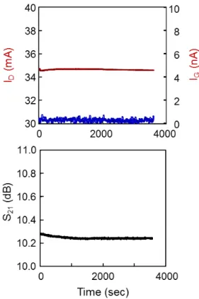
Fig. 14 Preliminary constant bias stress test result of GaN HEMT at room temperature. The gate length was 0.12µm with a gate width of 2
×50µm. The drain voltage was 10 V and a gate voltage of−0.5 V. S21was measured at 1 GHz.
millimeter-wave power amplifiers.
4. Bias Stress Test
The reliability of millimeter-wave GaN HEMTs has not been proved well. So we did a preliminary constant bias stress test as shown in Fig. 14. The gate length was 0.12 µm with a gate width of 2×50µm. The drain voltage was
ff T
of 113 GHz and maximum oscillation frequency fmax of 230 GHz were achieved. The output power density reached 1 W/mm with a gain of 6.4 dB at load-pull measurements at 90 GHz. And, we extracted the equivalent circuit model parameters and showed that the model was useful in simulat- ing millimeter-wave power performance of the InAlN/GaN HEMTs.
Acknowledgments
The research results have been achieved by “Agile De- ployment Capability of Highly Resilient Optical and Radio Seamless Communication Systems,” the Commissioned Re- search of National Institute of Information and Communica- tions Technology (NICT).
References
[1] H. Hayashi, Y. Nakasha, M. Aota, and N. Sato, “Millimeter-wave impulse radio technology,” FUJITSU Sci. Tech. J., vol.49, no.3, pp.350–355, 2013.
[2] K. Joshin, T. Kikkawa, H. Hayashi, T. Maniwa, S. Yokokawa, M. Yokoyama, N. Adachi, and M. Takikawa, “A 174 W high- efficiency GaN HEMT power amplifier for W-CDMA base station applications,” IEEE Int. Electron Device Meeting, Washington D.C., pp.12.6.1–12.6.3, Dec. 2003.
[3] T. Palacios, A. Chakraborty, S. Rajan, C. Poblenz, S. Keller, S. P.
DenBaars, J. S. Speck, and U. K. Mishra, “High-power AlGaN/GaN HEMTs for Ka-band applications,” IEEE Electron. Device Lett., vol.26, no.11, pp.781–783, Nov. 2005.
[4] Y. Nakasha, S. Masuda, K. Makiyama, T. Ohki, M. Kanamura, N. Okamoto, T. Tajima, T. Seino, H. Shigematsu, K. Imanishi, T.
Kikkawa, K. Joshin, and N. Hara, “E-band 85-mW oscillator and 1.3-W amplifier IC’s using 0.12-µm GaN MMICs for millimeter- wave transceivers,” IEEE CSIC Symp. Dig., Monterey, CA, pp.199–
202, Oct. 2010.
[5] A. Brown, K. Brown, J. Chen, K. C. Hwang, N. Kolias, and R. Scott,
“W-Band GaN power amplifier MMICs,” IEEE MTT-S Int. Microw.
Symp. Dig., Baltimore, MD, June 2011.
[6] M. Micovic, A. Kurdoghlian, A. Margomenos, D. F. Brown, K. Shi- nohara, S. Burnham, I. Milosavljevic, R. Bowen, A. J. Williams, P.
Hashimoto, R. Grabar, C. Butler, A. Schmitz, P. J. Willadsen, and D. H. Chow, “92–96 GHz GaN power amplifiers,” IEEE MTT-S Int.
Microw. Symp. Dig., Montreal, QC, Canada, June 2012.
[7] K. Shinohara, D. C. Regan, Y. Tang, A. L. Corrion, D. F. Brown, J. C. Wong, J. F. Robinson, H. H. Fung, A. Schmitz, T. C. Oh, S. J.
Kim, P. S. Chen, R. G. Nagele, A. D. Margomenos, and M. Micovic,
“Scaling of GaN HEMTs and schottky diodes for submillimeter- wave MMIC applications,” IEEE Trans. Electron. Dev., vol.60, no.10, pp.2982–2996, Oct. 2013.
[8] V. Tilak, B. Green, V. Kaper, H. Kim, T. Prunty, J. Smart, J. Shealy, and L. Eastman, “Influence of barrier thickness on the high-power performance of AlGaN/GaN HEMTs,” IEEE Electron. Device Lett.,
vol.22, no.11, pp.504–506, Nov. 2001.
[9] M. Higashiwaki and T. Matsui, “Barrier thickness dependence of electrical properties and DC device characteristics of AlGaN/GaN heterostructure field-effect transistors grown by plasma-assisted molecular-beam epitaxy,” Jpn. J. Appl. Phys., vol.43, no.9A/B, pp.L1 147–L1 149, Aug. 2004.
[10] Y. Yue, Z. Hu, J. Guo, B. Sensale-Rodriguez, G. Li, R. Wang, F.
Faria, B. Song, X. Gao, S. Guo, T. Kosel, G. Snider, P. Fay, D.
Jena, and H. G. Xing, “Ultrascaled InAlN/GaN high electron mo- bility transistors with cutofffrequency of 400 GHz,” Jpn. J. Appl.
Phys., vol.52, no.8S, pp.08JN14-1-2, May 2013.
[11] B. P. Downey, D. J. Meyer, D. S. Katzer, J. A. Roussos, M. Pan, and X. Gao, “SiNx/InAlN/AlN/GaN MIS-HEMTs with 10.8 THz·V Johnson figure of merit,” IEEE Electron. Device Lett., vol.35, no.5, pp.527–529, May 2014.
[12] J. Kuzmik, “Power electronics on InAlN/(In)GaN: Prospect for a record performance,” IEEE Electron. Device Lett., vol.22, no.11, pp.510–512, Nov. 2001.
[13] F. Medjdoub, M. Alomari, J.-F. Carlin, M. Gonschorek, E. Feltin, M. A. Py, N. Grandjean, and E. Kohn, “Barrier-layer scaling of InAlN/GaN HEMTs,” IEEE Electron. Device Lett., vol.29, no.5, pp.422–425, May 2008.
[14] T. Palacios, A. Chakraborty, S. Heikman, S. Keller, S. P. DenBaars, and U. K. Mishra, “AlGaN/GaN high electron mobility transistors with InGaN back-barriers,” IEEE Electron. Device Lett., vol.27, no.1, pp.13–15, 2006.
[15] D. S. Lee, B. Lu, M. Azize, X. Gao, S. Guo, D. Kopp, P. Fay, and T.
Palacios, “Impact of GaN channel scaling in InAlN/GaN HEMTs,”
IEEE Int. Electron. Device Meeting, Washington, DC, pp.457–460, Dec. 2011.
[16] C. F. Campbell, M. Y. Kao, and S. Nayak, “High efficiency Ka- band power amplifier MMICs fabricated with a 0.15µm GaN on SiC HEMT process,” IEEE MTT-S Int. Microw. Symp. Dig., Montreal, QC, Canada, June 2012.
[17] B. Heying, W. B. Luo, I. Smorchkova, S. Din, and M. Wojtow- icz, “Reliable GaN HEMTS for high frequency applications,” IEEE MTT-S Int. Microw. Symp. Dig., Anaheim, CA, pp.1218–1221, May 2010.
[18] Y.-F. Wu, A. Saxler, M. Moore, R. P. Smith, S. T. Sheppard, P. M.
Chavarkar, T. Wisleder, U. K. Mishra, and P. Parikh, “30-W/mm GaN HEMTs by field plate optimization,” IEEE Electron. Device Lett., vol.25, no.3, pp.117–119, Mar. 2004.
[19] I. Angelov, K. Andersson, D. Schreurs, D. Xiao, N. Rorsman, V.
Desmaris, M. Sudow, and H. Zirath, “Large-signal modelling and comparison of AlGaN/GaN HEMTs and SiC MESFETs,” Proc. of Asia-Pacific Microwave Conf. Yokohama, Japan, pp.279–282, Dec.
2006.
[20] Verilog-A definition of Angelov GaN FET in Agilent Advanced De- sign System (ADS) 2012.08.
Kazukiyo Joshin received the B.S. de- gree in physics from Kyoto University in 1978, the M.S. degree in physics from the Univer- sity of Tokyo in 1980, and the Ph.D. degree in electrical engineering from Osaka University in 1995. In 1980, he joined Fujitsu Laborato- ries Ltd., Kawasaki, where he worked on a re- search of low-noise HEMTs. He is currently engaged in research and development work on high-power and high-frequency GaN HEMTs at Fujitsu Laboratories Ltd., Atsugi. He received the Ichimura Award for his work related to the development of low-noise HEMTs in 1989. He is a member of the IEICE and IEEE.
Kozo Makiyama received the B.E. and M.E. degrees in electrical engineering from Os- aka Institute of Technology, Osaka, Japan, in 1986 and 1988, respectively. In 1988, he joined Compound Semiconductor Laboratory in Fu- jitsu Laboratories, Ltd., Atsugi, Japan, where he has been engaged in research and develop- ment of HEMT technologies. He is currently en- gaged in research and work on millimeter-wave device. Mr. Makiyama is a member of the Insti- tute of Electronics, Information and Communi- cation Engineers of Japan.
Shiro Ozaki received the B.S. and M.S.
degrees in applied chemistry from Yokohama National University, in 2002 and 2004, respec- tively. In 2004, he joined Fujitsu Laboratories Ltd., Atsugi, where he worked on a research of advanced materials for semiconductor devices.
He is currently engaged in research and devel- opment work on process technology for GaN- HEMT. He received the best presentation award from the ISPlasma in 2013.
Toshihiro Ohki received the B.E. and M.E.
degrees in Electrical Engineering from Waseda University, Tokyo, Japan, in 1999 and 2001, re- spectively. Since 2001, he was been with Fujitsu Laboratories Ltd., Atsugi, Japan, where he was engaged in the research and development of InP- based RTD/HEMTs and GaN-based HEMTs for high-speed optical and wireless communication systems. He is a member of the Japan Society of Applied Physics.
Naoya Okamoto received the B.E., M.E., and Ph.D. degrees from Osaka University, Os- aka, Japan, in 1988, 1990, and 2001, respec- tively. In 1990, he joined Fujitsu Laboratories Ltd. and developed carbon-doped GaAs-based HBT grown by gas-source MBE. Afterwards, he studied GaAs surface passivation using gal- lium sulfide and developed InP-based HEMT and RTD/HEMT circuits. Also, he had been a researcher of Nanoelectronics Collaborative Re- search Center of The University of Tokyo from 2002 through 2004. He is currently engaged in research and development of backside processing for GaN HEMT MMICs.
Yoshitaka Niida received the B.S., M.S. and Ph.D. degree in physics from Tohoku University in 2005, 2009 and 2012, respectively. In 2012, he joined Fujitsu Laboratories Ltd., where he is currently engaged in research and development work on GaN HEMT high power amplifiers.
Researcher’s Award from the IEICE in 2006.
Satoshi Masuda received the B.E., M.E., and Ph.D. degrees in electrical engineering from Waseda University, Tokyo, Japan, in 1995, 1997, and 2009, respectively. In 1997, he joined Fujitsu Laboratories, Kanagawa, Japan, where he has been engaged in research and develop- ment of millimeter-wave monolithic ICs. His current research interests include modeling of active and passive components, millimeter-wave monolithic IC design, and flip-chip packaging.
He received the Best Paper Award at the 2002 IEEE GaAs IC Symposium, the EuMC Microwave Prize at the 34th Euro- pean Microwave Conference (EuMC 2004), and the Young Scientists’ Prize by the Minister of Education, Culture, Sports, Science and Technology of Japan in 2006.
Keiji Watanabe received the B.E. and Ph.D.
degrees in Tokyo University of Agriculture and Technology, Tokyo, Japan in 1986 and 2006. He joined Fujitsu Laboratories Ltd., Atsugi, Japan in 1986, where he has been engaged in research and development of materials for microelectron- ics.

![Fig. 9 Equivalent circuit of the Angelov GaN HEMT model [20].](https://thumb-ap.123doks.com/thumbv2/123deta/5625864.1500206/4.892.467.814.116.431/fig-equivalent-circuit-angelov-gan-hemt-model.webp)