SUMMARY This paper describes latest RF Automated Test Equipment (RF ATE) technologies that include device under test (DUT) connections, a calibration method, and an RF test module mainly focusing on low cost of test (COT). Most important respect for low COT is how achieve a number of simultaneous measurements and short test time as well as a plain cali- bration. We realized these respects by a newly proposed calibration method and a drastically downsized RF test module with multiple resources and high throughput. The calibration method is very convenient for RF ATE.
Major contribution for downsizing of the RF test module is RF circuit tech- nology in form of RF functional system in package (RF-SIPs), resulting in very attractive test solutions.
key words: ATE, SoC tester, SIP, calibration, LTCC, MMIC
1. Introduction
By advanced CMOS-RF LSI, it is becoming possible to be one-chip integration of various wireless application such as wireless LAN and Bluetooth as well as cellular for 2G (GSM/EDGE), 3G (UMTS/WCDMA), and 3.9G (LTE) [1]–
[3]. Also, multiple-input multiple-output (MIMO) topolo- gies will become one of most promising solutions for im- proving the spectral efficiency of wireless systems [4], [5].
For ATE such as SoC testers, COT is vital as well as a mea- surement accuracy. Since the demand of reducing COT of RF test has been also increasing, simultaneous testing capa- bility and higher throughput are becoming most important specifications for an RF ATE.
For these requirements, several technical aspects for an RF ATE should be concerned. With respect to DUT boards, the stable correlation and repeatability while simul- taneous multi DUTs testing are often more important than to get extreme accurate data for low COT. A plane calibra- tion method also contributes to low COT. Since there are many RF ports that should be calibrated periodically, cali- bration time and its complexity affect the rate of uptime of an RF ATE. We propose a new calibration method special- ized for the RF ATE structure that derives a short calibra- tion time with a plane operation. To implement RF mul- tiple measurement resources with compact size, we con- structed an RF front-end with RF functional system in pack- age (RF-SIPs) instead of RF-HBICs. In addition, high speed switch MMICs for switches as well as for step attenuators using our accumulated GaAs high electron mobility tran-
Manuscript received November 28, 2011.
Manuscript revised April 1, 2012.
†The author is with Gunma Research and Development Center, Advantest Corporation, Gunma-ken, 370-0718 Japan.
a) E-mail: [email protected] DOI: 10.1587/transele.E95.C.1147
sistor (HEMT) technology have been incorporated. These technologies bring multiple resources integration and high test throughput with compact module size. In following sec- tions, we describe various kinds of technologies of latest RF ATE focusing on low test cost.
2. System Structure of RF ATE and Essential Issue with DUT Board Installation
2.1 Basic Structure of RF Test System
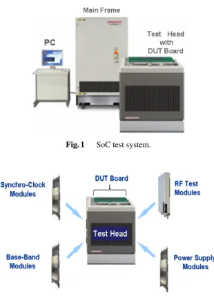
The photograph of our SoC test system and the basic con- struction of the test head for RF ATE are shown in Fig. 1 and Fig. 2, respectively. The SoC test system consists of the main frame, PC, and the test head. The main frame is a common instrument for various kinds of ATEs, and in- cludes a fundamental DC power supplies and liquid cooling sources. PC is for operations of the whole ATE system based on the OS specialized for the ATE. The test head plays a most important role of ATE systems, it determines the per-
Fig. 1 SoC test system.
Fig. 2 Test head construction.
Copyright c2012 The Institute of Electronics, Information and Communication Engineers
Fig. 3 Test diagram for transceiver devices.
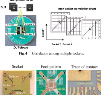
formances of RF ATE for RF-ICs testing. The test head consists of various kinds of modules and the DUT board. A testing block diagram of the test head with the RF ATE is depicted in Fig. 3. For testing of RF-LSI, an RF test mod- ule, a base-band (BB) module, a power supply (PS) module, and a synchro clock (SYC) module are installed. In case of DUTs with digital functions, a high speed digital mod- ule is also installed according to the required speed. Test cost mainly depends on test time. Therefore, simultaneous multi-die measurements and higher throughput per die are very important. Especially, the RF test module is the key module and required to have simultaneous testing capability and higher throughput. A high density construction of our new RF test module is described in Sect. 3.
The DUT board is an interface between each modules and DUTs. Extremely, performances of the RF interface be- tween the RF test module and DUTs is very important and a serious portion for the evaluation of DUT. Importance and difficulties on role of DUT boards associated with a calibra- tion method is substantial respect of RF testing. Therefore, the design of DUT boards and developments of an RF cal- ibration topology are also very important as well as the RF test module for reducing COT. Testing of RF-IC/RF-LSI in- cludes an evaluation of digital and baseband functions as well as RF characteristics.
2.2 Main Issue for DUT Board Simultaneous multi die testing
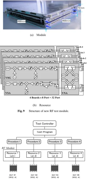
In order to comply with the requirement of reducing COT, we have to confront difficulties of the simultaneous multi- die measurements of RF-ICs. With respect to DUT boards, most serious problem is a correlation error among multi- die measurements as shown in Fig. 4. Major causes for the correlation error among multiple sockets are designated by following:
#1 Instability of socket pins to a DUT board contact
#2 Instability of RF connectors to a DUT board contact
#3 Imbalance of the pattern layout around the sockets
#4 Variations of component values for RF parts
A time-varying correlation error occurs often due to socket
Fig. 4 Correlation among multiple sockets.
Fig. 5 Pin contact condition.
pins to DUT board contact. Imbalance of the RF patterns around the sockets and of the RF ground condition for trans- mission lines, and variations of component values in RF parts of the matching circuits for the DUTs might affect a DUT dependent correlation error.
To keep a stable correlation among simultaneous multi DUTs, each layout of RF transmission lines for DUTs which include RF ground condition and matching accuracy should be designed as similar as possible. Since stability of pin contacts with sockets is very important for the repeatability of measurement, the adequate shape and metal materials of the socket pins should be concerned. The pin contact check at regular interval during test is also indispensable. The pin contacts condition is shown in Fig. 5.
Calibration
In a usual RF ATE, a calibration for correction of measure- ment errors is performed at module input/output (I/O) ports as reference planes. Then, an error correction between mod- ule I/O ports and DUTs is accomplished by embedding S- parameters of the DUT board with a corrective algorism.
The S-parameters must be known exactly, and then, imple- mented S-parameters should be valid during device testing.
Above conventional calibration method has serious prob- lems with the accuracy of error corrections and with the usability toward the operators. To guarantee the measure- ment accuracy of DUTs, a calibration should be executed at DUT ports as reference planes. Concerning these techni- cal backgrounds, we proposed a new calibration technique that is executed by a combination of the standard calibration (STD-Cal) and the frequency domain reflectometry calibra- tion (FDR-Cal). STD-Cal refers to the calibration at module I/O ports using open-short-load (OSL) method. As demon- strated in Fig. 6 and Fig. 7, FDR-Cal is the correction of transmission characteristics between module I/O ports and
Fig. 6 Definition of calibration reference plane.
Fig. 7 Reflection method.
Fig. 8 Verification of calibration algorithm.
DUT ports, using open-short (OS) method at DUT ports of the sockets. FDR-Cal allows moving calibration planes from module I/O ports to DUT ports with an easy process.
The verification of the new method is demonstrated in Fig. 8. By comparison before FDR-Cal and after FDR-Cal, it can be confirmed that this calibration method is very plain
multiple channel resources and higher throughput per chan- nel are rapidly increasing. Our conventional RF test mod- ules are composed of many RF-HBICs. An RF-HBIC is a large size high frequency component with coaxial connec- tors. And each of RF-HBICs is connected with RF cables such as semi-rigid cables. Therefore, the dimension of a module becomes large, and it becomes extremely difficult to install multiple resources into one module with small size.
In addition, RF attenuators that use mechanical RF switches have disadvantages of slow settling time besides large size.
The slow settling time cause low throughput. Our conven- tional RF test module consists of one vector signal generator (VSG) for a modulated signal generation, one vector signal analyzer (VSA) for a modulated signal analysis, and four vector network analyzers (VNA). In spite of non full mul- tiple resources, dimension of the RF test module becomes large size as 400 mm×480 mm×262 mm.
For these reasons, we have been facing difficulties in the realization of small size RF test module with complete 4 channel simultaneous measurement and high throughput per channel.
3.2 Advantage of New RF Test Module
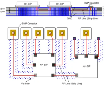
To overcome the problems mentioned above, we composed RF front-end of the new RF module with the RF-SIPs us- ing LTCC substrates instead of RF HBICs, and then, the RF test module is drastically downsized [6]. LTCC circuits are very adequate solution for small and medium volume applications [7], [8]. With regard to high throughput perfor- mances, we succeeded in the integration of RF step attenua- tor and single pole, four throw (SP4T) switch on one SIP by use of the developed high-speed step attenuator MMICs and SP4T switch MMIC, respectively. The high-speed MMICs can improve throughput of the RF test module, as being described in Sect. 4. An appearance of the new RF test module is shown in Fig. 9(a). It is equipped with 4 chan- nels for each of the resources of VSG, VSA and VNA. 2- tone signal output function is provided in the VSG. The re- source construction is shown in Fig. 9(b). The innovative RF-SIPs realize an RF test module that provide a 4 channel simultaneous full RF function measurement with volume of 480 mm×400 mm×72 mm. Since 4 resources are entirely independent, they can be assigned to the individual DUTs.
Figures 10 and 11 show multi-task capabilities performed by the 4 resources. In case of the testing for identical DUTs, each different test procedure can be executed. In the testing with different type of DUTs, the different test program can
Fig. 9 Structure of new RF test module.
Fig. 10 Module slice test performance — Testing same type of DUTs with different procedure.
be applied for each DUT. These functions are called “mod- ule slice” having an adaptive test capability and a multi-task test that provide decreasing test time and an effective test debug. Furthermore, throughput per channel is significantly improved as compared with our conventional RF test mod- ule.
3.3 RF-SIP and RF Board Construction
The RF front-end featuring large size metal housing package RF-HBICs with RF-connectors and coaxial cables brings excellent performances of isolation and transmission char- acteristics. On the other hand, the new configuration in form
Fig. 11 Module slice test performance — Testing different DUTs with different program.
Fig. 12 Structure of RF-SIP.
of RF-SIPs and RF boards has several design considerations for RF performances. Especially, problems of isolation be- tween inner circuits of RF-SIPs, and mismatch in ball grid array (BGA) connection between RF-SIPs and RF board are serious issues. The RF-SIP structure that realizes good iso- lation and passive circuit integrations is depicted in Fig. 12.
In this concept, semiconductor bare chip devices of high isolation required are mounted into small cavities of the LTCC substrate. The cavity is electrically sealed with inner metal cap whose rim is connected to ground through via holes. All of bare chips are mounted on the LTCC with face-up configuration, and are connected to microstrip lines using Au bond wires. Employing this SIP configuration, it is available to use various kinds of commercial and custom designed bare chips such as GaAs MMICs, Si-RFICs, and discrete devices. The SIPs also include several kinds of sur- face mount devices (SMD) to implement bias circuits and control circuits. 1005 and 0603 size SMD parts are mainly used. Precise RF passive circuits such as directional cou- plers, band-pass filters (BPFs) are also integrated inside of LTCC with strip line constructions. The SIPs are attached to the RF board using a solder reflow process with BGA in- serted between the SIPs and RF board. RF ground vias are arranged around RF signals to achieve a good impedance match and an enough isolation of RF signals. And many ground via are placed in around the center area of the LTCC to obtain the good RF ground condition and the thermal ra- diation as much as possible. As all kinds of SiPs are de- signed according to the same PIN assignment, we can evalu-
Fig. 13 Structure and pattern lazyout of RF board.
Fig. 14 Block diagram of RF board.
ate them with the particularly designed common RF socket.
Figure 13 demonstrates pattern layout of the RF board.
The RF transmission lines are strip line structure. The strip line structures, in which the RF signal is transmitted through an inner layer pattern, can achieve higher isolation than mi- crostrip lines. As with LTCC substrate, at area of the RF pat- tern, many ground via holes are deposited in short pitch in order to suppress waveguide mode and parallel plate mode.
Dimension of all the RF-SIPs mounted on the RF boards is 20 mm×20 mm×3 mm. 14 RF-SIPs are mounted per one RF board as shown in Fig. 14.
3.4 Down Sizing Example of RF SiP
Figure 15 exhibits the comparison of the RF HBIC and the RF SiP. Each of them has the same function as VNA includ- ing one directional coupler, two isolation amplifiers, and two down convert mixers. By applying RF SiP, the volume of VNA function block can be drastically down sized less than 1/66 compared with our conventional RF HBIC.
Fig. 15 Comparison of RF HBIC and RF SiP.
4. High Speed Switch Technologies for High Through- put
To realize high throughput of the RF test module, high- speed switching operation of switches for transmission path control and step attenuators for RF power level control is one of most important characteristics. In addition, high iso- lation is also very important for switches and step atten- uators. HBICs using discrete bare chips are very attrac- tive to achieve high isolation performance, but are not suit- able for compact size. PIN diode switches are usually used for measurement instruments because of their fast switch- ing performance, but they do not accomplish the require- ments of smaller size and lower power consumption. GaAs MMIC switches are suitable for compact size and small power consumption, but are not adequate for fast switching required for ATE. To eliminate these dilemmas, we realized high speed switch MMICs and step attenuator MMICs us- ing newly established HEMT process having on/offsettling times on the order of several microseconds.
High-speed switching HEMTs
As shown in Fig. 16, the settling time definition for RF ATE is the time required for the output power to go from 0 to 99.9% when the control voltage is switched. For the switches using conventional HEMT devices, the settling time from 10 to 90% is very fast in order of a few nanosec- onds. However, at 0 to 99.9%, a well-known phenomenon called gate lag caused delays in order of several millisec- onds to as long as several seconds. In order to obtain high throughput of RF test, it is crucial that all the circuits have fast switching times. Then, we developed a proprietary HEMT process based on the particular deposition technol-
Fig. 16 Definition of settling time.
Table 1 Comparison of settling time for HEMTs.
ogy for a passivation layer that derives significant improve- ment on switching speed. Table 1 presents a comparison of settling time for HEMT devices. The new type one has a settling time of about 50µs.
High speed switch and step attenuator MMICs
The designed two types of switch MMICs and three types of step attenuator MMICs are indicated by shading in the illustration of Fig. 14. Selects of transmission path are performed by two types of switches, single pole, double throw (SPDT) switches and single pole, four throw (SP4T) switches. For signal level control, on the other hand, three types of step attenuator with an attenuation of 40 dB, 35 dB, and 28 dB are used. The frequency range of MMICs is 100 MHz to 12 GHz.
Figures 17 and 18 show photographs of the SP4T switch and the 35 dB step attenuator MMICs. Both chip size are 1.2 mm×2.4 mm. The configuration employs an el- ementary combination of series/shunt HEMT devices. Fig- ure 19 exhibits the measured and simulated insertion loss and isolation of the SP4T switch. It can be seen that there is close between the measured and simulated results. The in- sertion loss of less than 1.8 dB and the isolation of more than 63 dB are achieved across a frequency band of 100 MHz to 12 GHz.
Figure 20 indicates the switching speed of the SP4T switch. The settling time is 50µsec, which is the same as for the HEMT devices themselves, and exhibit a significant im- provement as compared with the conventional switches. The newly designed five types of MMICs have same high speed switching performance. The designed 40 dB, 35 dB, and 28 dB step attenuator have also very first switching speed same as switch MMICs.
Thanks to these high speed MMICs, and by adding improvement of frequency settling of the RF synthesizer,
Fig. 17 Photograph of SP4T-switch.
Fig. 18 Photograph of 35 dB step attenuator MMIC.
Fig. 19 Measured and simulated result of SP4T switch.
Fig. 20 Switching speed of SP4T switch.
the throughput per channel becomes less than 1/5 compared with our conventional module.
5. Performances of the RF ATE
Table 2 summarizes typical specifications of the RF ATE.
For the VSG, the minimum output power of less than
−120 dBm and the maximum output power of more than +5 dBm are achieved across a frequency band of 100 MHz to 6 GHz. The noise floor of the VSA is −153 dBm at 2.2 GHz. As compared with our conventional RF test mod- ule, the settling time at the instantaneous frequency change is extremely improved from 800µs to 150µs.
6. Conclusions
In this paper, we introduced recent RF ATE technolo- gies which include the DUT board, the calibration method as well as high density construction of RF test mod- ule. The RF test module is a fully 4 channel of VSA, VSG, and VNA having 32-ports with dimension of 480 mm×400 mm×72 mm. The volume is reduced about of 1/15, and the throughput per channel becomes less than 1/5 compared with our conventional module. Our new RF ATE will enable to reduce COT drastically, and provide con- venient testing solutions featuring the adaptive test and the multi-task test by full resources structure.
References
[1] R. Koller, T. Ruhlicke, D. Pimingsdorfer, and B. Adler, “A single-chip 0.13µSIPOS UMTS W-CDMA multi-band transceiver,” 2006 IEEE Radio Frequency Integrated Circuits Symposium, June 2006.
[2] J.-W. Lai, C.-H. Wu, A. Lin, W.-K. Hong, C.-Y. Wang, C.-H. Shen,
[5] K. Lim, S. Min, S. Lee, J. Park, K. Kang, H. Shin, H. Shim, S. Oh, S.
Kim, J. Lee, C. Yoo, and K. Chun, “A 2×2 MIMO tri-band dual-mode direct conversion CMOS transceiver for worldwide WiMAX/WLAN applications,” IEEE J. Solid-State Circuits, vol.46, no.7, pp.1648–
1658, July 2011.
[6] M. Kimishima, “Introduction to latest RF test technologies in RF ATE for low test cost,” 2011 China-Japan Joint Microwave Conference Proceedings, April 2011.
[7] Y.C. Lee, W.I. Chang, and C.S. Park, “Monolithic LTCC SiP trans- mitter for 60 GHz wireless communication,” 2005 IEEE MTT-Symp.
Digest, pp.1015–1018, 2005.
[8] T. Baras and A.F. Jacob, “Integrated LTCC synthesizer and signal con- verter module at K-band,” IEEE Trans. Microw. Theory Tech., vol.57, no.1, pp.71–79, Jan. 2009.
Masayuki Kimishima received the B.S.
degrees in Electrical Engineering from Niigata University, Niigata, Japan. He joined Tokyo Keiki Inc. in 1984, where he was involved in the development of broadband microwave cir- cuits for aero-defense systems. In 1994, he joined New Japan Radio Corporation, where he has worked on the development of MMICs for mobile communications. In 1998, he moved to ADVANTAST Corporation, where he has been engaged in the development of microwave and millimeter-wave MMIC for measurement instruments, and automated test equipments. He is a member of the IEEE.