INVITED PAPER
Special Section on Microwave and Millimeter-Wave TechnologyScattered Reflections on Scattering Parameters
—Demystifying Complex-Referenced S Parameters—
Shuhei AMAKAWA†a),Member
SUMMARY The most commonly used scattering parameters (S pa- rameters) are normalized to a real reference resistance, typically 50Ω. In some cases, the use of S parameters normalized to some complex reference impedance is essential or convenient. But there are different definitions of complex-referenced S parameters that are incompatible with each other and serve different purposes. To make matters worse, different simulators implement different ones and which ones are implemented is rarely prop- erly documented. What are possible scenarios in which using the right one matters? This tutorial-style paper is meant as an informal and not overly technical exposition of some such confusing aspects of S parameters, for those who have a basic familiarity with the ordinary, real-referenced S pa- rameters.
key words: S parameters, reflection coefficient, transmission coefficient, traveling waves, pseudo waves, power waves, reference impedance, renor- malization transformation
1. Introduction
According to Carlin[1], the earliest article that dealt with the scattering parameters or S parameters was[2], published in 1920. The first book[3]that gave extensive coverage of the subject was published in 1948[1]. The S parameters described in this book are essentially the same S parameters as those we most often (but not always!) use today. Those are the real-referenced S parameters.
To define S parameters, we must first define an effec- tive voltage and an effective current from the electric and magnetic fields in a waveguide, respectively. A “wave- guide” here may refer to a (quasi-)TEM (transverse electro- magnetic) transmission line, a hollow metallic waveguide, or some other form of waveguide. In the case of ideal TEM transmission lines, the mapping of electromagnetic (EM) fields to voltages and currents is unique. But in general, there is some arbitrariness in the mapping. This arbitrariness implies that there is arbitrariness in the definition of charac- teristic impedance, too. We don’t delve here into the diffi- cult and controversial problem of how the mapping should be done[4]–[8], and simply assume that effective voltage and current have been defined appropriately. We will here- after refer to them simply as “voltage” and “current,” respec- tively. We will also assume that our waveguide is a quasi- TEM transmission line.
Now that we have voltages and currents in waveguides Manuscript received February 15, 2016.
Manuscript revised June 27, 2016.
†The author is with the Graduate School of Advanced Sciences of Matter, Hiroshima University, Higashihiroshima-shi, 739–8530 Japan.
a) E-mail: [email protected] DOI: 10.1587/transele.E99.C.1100
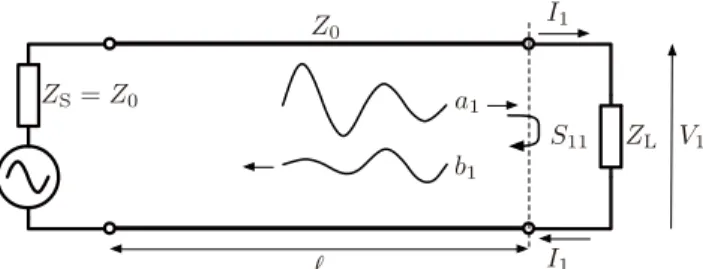
Fig. 1 A length, , of transmission line driven by a matched source (source impedanceZS = Z0) and terminated with a load impedanceZL. Z0is the characteristic impedance of the line.
somehow defined, can we define S parameters uniquely?
Not yet. We have a choice between defining S parameters, including reflection coefficients, based on voltages or cur- rents. The choice may[3],[9]–[13]or may not[14]affect the values of S parameters, depending on how you define current scattering parameters. We opt for the voltage-based definition, as is commonly practiced.
If a transmission line is terminated with an impedance ZLas shown in Fig. 1, thevoltagereflection coefficient at the terminating load is[11]–[13]
S11= ZL−Z0
ZL+Z0, (1)
where Z0 is the characteristic impedance of the line. Z0
appears in Eq. (1) because the reflection coefficient is a description of a 1-port in question (in this case, the load impedanceZL) in terms of incident and reflected traveling wave amplitudes in a one-dimensional medium (i.e. trans- mission line) that feeds the 1-port.Z0is a physical property of the one-dimensional medium, not of the 1-port. The stan- dard assumption, often made implicitly, is that the transmis- sion line is lossless, and thereforeZ0 is real. Its standard value is 50Ω[15],[16]. To emphasize the fact that the value of S11 depends onZ0, and that its value is real, it is more appropriate to write instead
S11 (Rref) =ZL−Rref
ZL+Rref. (2)
The above notation of explicitly showing the reference re- sistance Rref of an S parameter in parentheses was intro- duced by Woods[17]. The notation is summarized in Ta- ble 1. The standard choice ofRrefis thecharacteristic resis- tance[18],[19]R0 of the lossless transmission line, which the loadZLterminates. Why don’t we simply writeS11 (R0)? Copyright c2016 The Institute of Electronics, Information and Communication Engineers
Table 1 Notation for showing reference impedances.
Example Description
Si j(50Ω) S parameter with portsiandjreferenced to 50Ω S(Rref) S matrix with all ports referenced toRref
S21 (Rref1,Rref2) Port 1 referenced toRref1, port 2 referenced toRref2
S(Zref1,Zref2) 2-port S matrix referenced toZref1andZref2
S(Zref) S matrix referenced to reference impedance matrix Zref=diag(Zref1,Zref2,· · ·)
Well, we could, but we might want to use an Rref value different than R0, which is a property of the transmission line. In some situations, we might want to assign toRref a value that isnota property of a physical object (transmis- sion line) at hand. We will later see when such a need arises (§3.1). The characteristic resistance and the reference resis- tance should not be mixed up.
In the real world, all transmission lines are lossy, at least to a small degree. Then, the characteristic impedance Z0 expressed in terms of the per-unit-length RLGC param- eters,
Z0=
R+jωL
G+jωC, (3)
assumes acomplexvalue, unless the the distortionless con- dition[9],[11],[20],
R L =G
C, (4)
is met. What happens, then, to the reflection coefficient?
Can we keep using Eq. (1) or (2) with a complexZref(refer- ence impedance) substituted forRrefas follows,
S11 (Zref)= ZL−Zref
ZL+Zref, (5)
or do we need something different? It is curious that most microwave textbooks refer to the complex characteristic impedance formula, Eq. (3), yet many of them are silent about how to define reflection coefficients and S param- eters whenZ0orZref is complex. Even microwave metrol- ogists don’t appear to have looked very seriously into the issue[21], perhaps till mid 1980s.
Another question that springs to mind in this connec- tion is this: how does the definition ofS11with a complexZ0
relate to the well-known textbook problem (Fig. 2) of maxi- mizing the power absorbed (and dissipated) by a loadZLfed by a signal source with an impedanceZS? We all know that, to maximize the power absorbed by the load in Fig. 2, the load impedanceZL and the source impedanceZS must be complex conjugate of each other (ZL =Z∗S). DoesS11 =0 (defined in what way?) imply that the power absorbed by the load in Fig. 1 is maximized? This question is not as trivial as it might appear (§2.5).
In this article, we look at complex-referenced S pa- rameters. There are, at least, two distinct definitions of complex-referenced S parameters. They are incompatible with each other and serve different purposes. Depending
Fig. 2 A Th´evenin signal source with an impedanceZS feeds a load impedanceZL. How can the power absorbed (dissipated) by the load be maximized?
on the system under consideration, the appropriate one to use differs. The most appropriate value to use as the refer- ence impedanceZrefmight be the characteristic impedance Z0that feeds the network, the source impedanceZSthat di- rectly feeds the network, or some other value. You might possibly think that complex-referenced S parameters are a matter of purely academic concern with little practical use.
But that is not so. We work on millimeter-wave CMOS cir- cuit design[22]–[29] and related measurements[30]–[42], and regularly use bothtypes of complex-referenced S pa- rameters out of necessity. Situations in which using the right one would matter include millimeter-wave and terahertz on- wafer measurements, where methods of vector network ana- lyzer (VNA) calibration and de-embedding that work well at lower microwave frequencies fail. Also relevant would be power transfer systems, in which long transmission lines are deployed and minimizing losses is imperative. It is un- fortunate that, in spite of the practical importance of the sub- ject, resources are largely limited to research papers scat- tered about everywhere (a recent exception is[43]), at times with somewhat biased views.
To make matters worse, microwave engineers are left with microwave simulators, EM simulators and related programs that are strangely silent about which complex- referenced S parameters they implement (if they do), or whether they do. It is practically very important that you understand which S parameters you want to use and which ones your simulator implements. I hope this article helps develop practicing microwave engineers’ awareness of the potential dangers of using wrong S parameters in the wrong context. This article was derived from an article that I pre- sented at MWE 2015[44], which, in turn, was based upon a tutorial that I gave in 2011[45]. Articles that discuss related issues include[4],[17],[46]–[51].
2. Two Definitions of Reflection Coefficients
A reflection coefficient is the S parameter of a 1-port. We can learn a great deal about S parameters by looking at re- flection coefficients.
2.1 Transmission Line and Reflection Coefficients If the far end of a length of lossy transmission line is ter- minated with its complex characteristic impedance Z0 as shown in Fig. 3, the line looks as if it were infinitely long (Zin = Z0) as seen from the near end. It means that no
Fig. 3 A length of transmission line terminated with its characteristic impedanceZ0at the far end looks as if the line were infinitely long as seen from the near end.Zin=Z0andS11 (Z0)=0.
waves reflect back when injected traveling waves reach the far end. The reflection coefficient S11 at the terminating load, ZL = Z0, must be equal to 0. IfZL Z0, S11 will be nonzero. We, therefore, adopt Eq. (5) withZref = Z0 to define the reflection coefficient of a 1-port ZL that termi- nates the transmission line. If the terminating load has an impedanceZL Z0, reflected waves come back to the near end, and the line no longer appears infinitely long. The re- flection coefficient, defined as above, is a representation of a 1-port in terms of traveling-wave amplitudes that appear in a transmission line, through which the 1-port is excited.
That’s why a property, Z0, of the transmission line enters the expression, Eq. (5), throughZref =Z0. The characteris- tic impedance of the line physically connected to the load is thenatural reference impedance(my preferred term) in this case. It is a property of the physical (as opposed to a virtual) environment in which the network in question is embedded.
It is, however, not clear from Eq. (5) what the incident and reflected waves are. Equation (5) is a voltage reflection coefficient as noted in§1. Specifically,
S11 (Zref)≡ V1− V1+ =b1
a1, (6)
where V1+ is the complex amplitude of the rightward- traveling wave incident upon the load, V1− is that of the leftward-traveling, reflected wave. While V1+ andV1− are sufficient for defining a reflection coefficient, with a view to smooth extension to multiports†, normalized wave ampli- tudes,a1andb1, are usually used[4].
a1≡
(Zref)
|Zref| V1+=
(Zref)
|Zref|
V1+ZrefI1
2 , (7)
b1≡
(Zref)
|Zref| V1−=
(Zref)
|Zref|
V1−ZrefI1
2 , (8)
a1 and b1 are termed pseudo waves[4], because when Zref assumes a value different than the natural reference impedance (i.e. characteristic impedanceZ0of the physical
†If a scattering matrix is defined using voltage amplitudesVi+ andV−j, a reciprocal network’s S matrix becomes symmetric only if reference resistances of all ports are equal[12],[52],[53]. Ifaiand bjare used instead to define an S matrix, a reciprocal network’s S matrix becomes symmetric even when reference resistances are not all equal. But if reference impedances are complex, a reciprocal network’s S matrix may be asymmetric.
transmission line that feeds the network),a1andb1(andV1+ andV1−, too) are no longer directly related to the voltage- and current-traveling-wave amplitudes in the line. Only when ZrefequalsZ0doa1andb1 correspond to actual traveling- wave amplitudes in the transmission line. But hereafter, we conveniently forget the fictitious nature of pseudo waves, and pretend that they are related to voltage- and current- traveling-wave amplitudes.
The port voltageV1 and the port currentI1at the load are related to the voltage- and current-traveling-wave ampli- tudes as
V1=V1++V1−, (9)
I1 =I+1 +I1−. (10)
The characteristic impedance relates the voltage- and current-traveling-wave amplitudes traveling in the same di- rection:
V1+ I1+ =−V1−
I1− =Z0(=Zref). (11) Z0being complex (argZ0 0) means that there is a phase difference between the voltage and current traveling waves.
Althougha1andb1have the dimensions of square root of power, they are just voltages multiplied by a real number, (Zref)/|Zref|, as is clear from Eqs. (7) and (8). They are, therefore, essentially voltages, and the reflection coefficient, Eq. (6), should be understood as avoltagereflection coeffi- cient. IfZrefis real (Zref =(Zref)=Rref), Eqs. (7) and (8) reduce to the widely known formulas:
a1= V1+
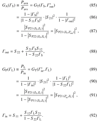
√Rref
=
RrefI+1 = 1
√Rref
V1+ZrefI1
2 , (12)
b1= V1−
√Rref
=−
RrefI1−= 1
√Rref
V1−ZrefI1
2 . (13)
a1 andb1 are often mixed up in the literature with power waves(Eqs. (19) and (20))[54], which we will be discussing in§2.3. While it is not incorrect to regard Eqs. (12) and (13) as power waves, given the fact that Eqs. (19) and (20) reduce to Eqs. (12) and (13) for realZref, I would like to emphasize thata1andb1are voltage waves, expressed in square root of watts.
2.2 Current Reflection Coefficients
The real-referenced current reflection coefficient of a load ZL(Fig. 1) is given usually[3],[9]–[13]by
SI11 (Rref)=−S11 (Rref) =−ZL−Rref
ZL+Rref. (14) This follows from
SI11 (Rref)≡ I1− I1+ =−b1
a1, (15)
where we used Eqs. (12) and (13). Its complex-referenced
extension isSI11 (Zref) =−S11 (Zref).
Less common but another valid definition of current re- flection coefficient is[14]
SI11 (Rref) ≡ I−1 I1+ = b1
a1 =S11 (Rref)= ZL−Rref
ZL+Rref, (16) where, I−1 = −I1−, and the port current is given by I1 = I1+−I1−, instead of Eq. (10). This amounts to accounting for the direction of reflected current “outside”I1−. This not so popular definition is not completely worthless, because Eq. (16) is actually consistent with the power-wave reflec- tion coefficient, Eq. (21), which is a current reflection coef- ficient (§2.7,§2.8).
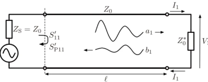
2.3 Reflection Coefficient for Power Maximization Let’s get back to Fig. 2 and think about how a reflection co- efficient should be defined if we want it to be zero when the power absorbed by the load is maximized. SinceZL =ZS∗is the condition for power maximization, an appropriate defi- nition of the reflection coefficient would be
SP11 (Zref)= ZL−Z∗ref
ZL+Zref (17)
withZref = ZS. A subscript ‘P’ is added to the left-hand side of Eq. (17) to make it distinguishable from Eq. (5). Re- flection coefficients of this type can be traced back to[55].
Equation (17) reduces to Eq. (2) whenZref is real. When SP11 (ZS) = 0, the power absorbed by the load ZL is maxi- mized, and the absorbed power equals the available power, Pavs, of the signal source.
Pavs≡|ES,rms/2|2
(ZS) = |ES|2
8(ZS). (18)
ESis the amplitude of the voltage source in Fig. 2, andES,rms is its root-mean-square (rms) value. The “waves” incident upon the load and reflected back in Eq. (17) are[54],[56]–
[58]
ap1= 1 (Zref)
V1+ZrefI1
2 , (19)
bp1= 1 (Zref)
V1−Zref∗ I1
2 , (20)
SP11 (Zref)= bp1
ap1. (21)
ap1 andbp1are usually referred to as thepower waves[54], although they have the dimensions of square root of power.
As mentioned earlier, Eqs. (7) and (8) are not power waves.
2.4 Power Absorbed by a Load
What about the power,PL, absorbed by the load in Fig. 1?
From Eqs. (6) through (10), we get PL= (V1I1∗)
2 = [(V1++V1−)(I1++I−1)∗]
2 (22)
Fig. 4 A length of transmission line terminated with the complex conju- gate,Z∗0, of the characteristic impedanceZ0.
= 1 2
|a1|2− |b1|2−2(a∗1b1)(Zref) (Zref)
(23)
= |a1|2 2
1−S11 (Zref)2−2
S11 (Zref) (Zref) (Zref)
. (24)
Note that in this articleV1 andI1 are amplitudes, not rms values. If Zref is real, the last terms in Eqs. (23) and (24) disappear, and we obtain the well-known result:
PL=1
2 |a1|2− |b1|2
=1 2|a1|2
1−S11 (Rref)2
, (25)
wherea1andb1are given by Eqs. (12) and (13). In Eq. (25),
|a1|2/2 and |b1|2/2 can be interpreted as incident and re- flected powers, respectively, and |S11|2 can be understood as the reflection coefficient for power. In contrast, when Zref is complex, the last term in Eq. (24) kicks in, and
|a1|2/2 and |b1|2/2 can no longer be interpreted as pow- ers[10],[52],[59]. This might appear undesirable proper- ties ofa1andb1as defined by Eqs. (7) and (8).
On the other hand,ap1 andbp1 are defined so that the same form as Eq. (25) results even whenZrefis complex:
PL= 1
2 |ap1|2− |bp1|2
= 1 2|ap1|2
1−SP11 (Zref)2
. (26)
This is highly pleasing compared to the seemingly awkward Eq. (24), and thereafter, power-wave S parameters became network theorists’ favorite definition of complex-referenced S parameters[52],[60],[61]. Power-wave S parameters also saw widespread adoption by microwave engineers, too[12], [14],[62]–[65]. But as we will see, the pleasing property comes at a price. At this point, I only point out the fact that the last term in Eq. (24) can’t be nulled out; it still lurks in Eq. (26). Otherwise, the conservation of energy would be violated. In this sense, nothing is fundamentally wrong with Eq. (24). Also note that in Eq. (26) the reflection coefficient for power is the scalar quantity|SP11|2, not the complexSP11. The physical meaning of its phase, argSP11, is not as clear as argS11[48],[65].
2.5 Transmission Line Terminated withZ0∗
What if the terminating load impedance in Fig. 1 isZL = Z∗0, as shown in Fig. 4? Looking leftward into the line from the load, the input impedance isZ0. The natural reference impedance there, therefore, is Zref = Z0 for both S11 and
Fig. 5 A length of transmission line terminated with its characteristic impedanceZ0. Traveling waves emanating from the signal source are ab- sorbed by the loadZ0without any reflection.
Fig. 6 Input reflection coefficientsS11andSP11at the left end of the line.
SP11. Since Fig. 5 corresponds to the case whereS11 (Z0)=0, S11 (Z0) 0 in the case of Fig. 4. To be more specific, the voltage reflection coefficient of the loadZ0∗is, from Eq. (5),
S11 (Z0) =Z0∗−Z0
Z0∗+Z0 =−jX0 R0
(Fig. 4), (27)
where Z0 = R0 +jX0. This means that the line wouldn’t appear infinitely long as seen from the signal source. How- ever, since the leftward and rightward input impedances at the load are, respectively,Z0andZ0∗, the power-wave reflec- tion coefficient of the load is, from Eq. (17),
SP11 (Z0)= Z0∗−Z0∗
Z0∗+Z0 =0 (Fig. 4). (28) This means that the power PL (Eq. (26)) absorbed by the load is maximized. But wait. In Fig. 5 (not Fig. 4), all traveling waves are absorbed by the load as suggested by S11 (Z0) =0. Equation (24) withS11 = 0 seems to suggest thatPLis maximized in the case of Fig. 5, too. What’s going on here?
The short answer:|ap1|2/2=Pavs>|a1|2/2; see the first terms of Eqs. (24) and (26). The power flowing out from the signal source in Fig. 5 is less than its available power, Eq. (18). In this rough sketch, we pretended that → 0 and ignored the power dissipated by the lossy transmission line itself. That must, of course, be taken into consider- ation in practice in power transfer problems. What is the actual power available at the right end of the transmission line in Fig. 4? It must be less thanPavs. Even at the left end of the line in Fig. 4, the power that flows into the line should, in general, be less thanPavs due to the mismatch there (SP11 (Z S) 0 in Fig. 6). How can that power be made
Fig. 7 A passiveZL’s range of argZLon an impedance plane.|argZL| ≤ π/2.
equal toPavs? Perhaps by changing the load fromZ0∗? What happens then toS11andSP11at the right end of the line?
2.6 Moduli of Reflection Coefficients
Most textbooks state that the modulus of a passive load’s (ZLwith(ZL) ≥0) reflection coefficient is at most unity.
This statement is valid for reflection coefficients defined by Eq. (2) or (17), but not for Eq. (5). If Zref is complex,
|S11 (Zref)| might become greater than unity (|S11 (Zref)| > 1) even if ZL is passive. In contrast, Eq. (17) always satis- fies|SP11 (Zref)| ≤1 for passiveZL, which, again, might give the impression that power waves, Eqs. (19) and (20), are su- perior to pseudo waves, Eqs. (7) and (8).
Let’s look more closely at what this is about[59]. Let zL≡ ZL
Zref. (29)
Then, from Eq. (5), S11 (Zref)= zL−1
zL+1. (30)
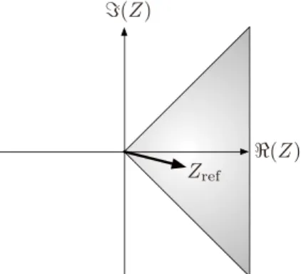
Since(ZL)≥0 by passivity assumption,|argZL| ≤π/2, as shown in Fig. 7. LetZref=Z0, whereZ0is given by Eq. (3).
Assuming that our transmission line is an ordinary right- handed line[66]withR,L,G,C >0, we have(Zref) >0.
Since the complex square root function is given by z1/2=±
|z|exp
jargz 2
, (31)
|argZref|< π/4 as shown in Fig. 8. From Eq. (29) and Figs. 7 and 8, we get
|argzL|<3π
4 , (32)
as shown in Fig. 9. Let us now take a look at the numera- tor and the denominator of Eq. (30) on a complex plane (Fig. 10). It is geometrically clear from Fig. 10 that|zL−1| can be greater than|zL+1|, and hence|S11|>1 is possible.
Analytically,
|S11 (Zref)|2= zL−1 zL+1·z∗L−1
z∗L+1 =|zL|2+1−2(zL)
|zL|2+1+2(zL). (33)
Fig. 8 The range of argZref on an impedance plane whenZref = Z0.
|argZref|< π/4.
Fig. 9 The range of argzL, defined by Eq. (29), on a complex plane.
|argzL|<3π/4.
Fig. 10 Eq. (30)’s numeratorzL−1 and the denominatorzL+1 on a complex plane.
(zL) in Eq. (33) can be positive or negative because of Eq. (32).|S11 (Zref)|>1 results if(zL)<0.
The fact that|S11 (Zref)|can exceed unity even for a pas- sive load has long been known[10],[11],[59],[67]–[70], but unfortunately, only to not so many of those who have known it. It is also well understood that no laws of physics are violated even when|S11 (Zref)| > 1, however uncomfort- able you might feel with it. The theoretical maximum value of|S11 (Zref)|is stupendous 1+ √
2 2.41[59]! In reality,
|(Z0)| is usually a small fraction of(Z0) (> 0), and the values of|S11 (Z0)|(>1) we encounter in real life (measure- ments especially) will be fairly close to unityexcept at very
Fig. 11 A Norton signal source with an admittanceYS feeds a load impedanceZL.
low frequencies[67]. A|S11 (Zref)|value significantly greater than unity might, therefore, be an artifact of unrealistic sim- ulation, for example. But any discomfort associated with even the slightest deviation from|S11 (Zref)| ≤1 might as well be an “artifact” of human mind, because no laws of physics demand that|S11 (Zref)| ≤1.
2.7 Smith Chart and Reflection Coefficients
The result of§2.6 immediately leads to a disturbing conclu- sion: IfZrefis complex, a locus of a passive load’sS11 (Zref)
can stray out of the unit circle on a Zref-centered Smith chart[69]. Note also thatZref = Z0 is usually frequency- dependent, which might be another nuisance.
Given the fact that |SP11 (Zref)| ≤ 1 for passive loads, you might expect SP11 (Zref) helps here too. But it’s not that simple. Recall that the Smith chart is derived from Eq. (5). Since Eq. (17) is different from Eq. (5), we can- not plot SP11 (Zref) on a Smith chart in the usual way we know. Let’s consider an ideal “short” (ZL = 0). We all know that short’s reflection coefficient is S11 = −1. This (S11 (Zref)=−1) is valid whether or notZrefis real in Eq. (5).
But we get from Eq. (17) andZL=0 SP11 (Zref) =−Zref∗
Zref (short). (34)
Evidently,SP11 (Zref) −1 unlessZrefis real. This appears to go against microwave engineer’s common sense. Now, how can we plotSP11 (Zref)on a Smith chart? Note that[54],[64]
SP11 (Zref)= [RL+j(XL+Xref)]−Rref
[RL+j(XL+Xref)]+Rref = ZL −Rref
ZL +Rref, (35)
Zref=Rref+jXref, (36)
ZL≡RL+j(XL+Xref). (37) Equation (35) has the same form as Eq. (5). By plottingZL instead ofZL on anRref-centered Smith chart, we can find the absolute value and the argument ofSP11 (Zref). Note that Rrefwill often be frequency-dependent.
But this is not the whole story. The above is valid if the signal source is a Th´evenin equivalent as in Fig. 2. But if you start the theoretical development from a Norton-type signal source (Fig. 11), you can get a different conclusion! It can be shown that (see[48]and Appendix F of[65]) another possible and perfectly valid definition of the power-wave re- flection coefficient is
SPV11 (Zref) =Zref
Z∗ref ·ZL−Zref∗ ZL+Zref = Zref
Zref∗ SP11 (Zref). (38) The ‘V’ in the subscript indicates that this reflection coef- ficient is a voltage reflection coefficient. Although I didn’t explain this, contrary to popular belief,SP11 (Zref) should be understood as a current reflection coefficient[48] (§2.8).
Equation (17) reduces to Eq. (16) whenZrefis real. Equa- tion (38) follows from a somewhat different definition of power waves than Eqs. (19) and (20):
ap1= 1 (Yref)
I1+YrefV1
2 , (39)
bp1= 1 (Yref)
I1−Yref∗ V1
2 , (40)
SPV11 (Yref) ≡bp1
ap1. (41)
Yref = 1/Zref is the reference admittance. From Eq. (38), short’s reflection coefficient isSPV11=−1! This might ap- pear more desirable than Eq. (34). However, the definition Eq. (41) is rarely adopted in practice.
In any case, why does such arbitrariness in the defi- nition of power waves and associated SPparameters arise?
Th´evenin and Norton signal sources are just two equiva- lent representations of the same physical source. Note that
|SP11 (Zref)| = |SPV11 (Yref)|and that the arbitrariness is in the phase. This is related to the remark made at the end of§2.4.
Other definitions than Eqs. (21) and (41) are also possible.
For example, yet another valid current-based definition of power-wave reflection coefficient is
SPI11 (Zref) =−SP11 (Zref) =−ZL−Z∗ref
ZL+Zref. (42) Equation (42) reduces to Eq. (14) whenZref is real. It can further be shown that[51] the choice of phases of power waves is arbitrary. What does this physically mean?
2.8 Measurable Waves and S Parameters
Measurement is the act of sensing some physical quantities.
As noted in§2.1, Eqs. (7) and (8) withZref =Z0are physi- cal voltage traveling waves (multiplied by a real constant), and therefore these are measurable complex (phasor) quan- tities. Receivers in a calibrated VNA sense mathematically transformed version of these waves. Modern VNAs adopt analog-to-digital converters for voltage measurements[71].
What about the power waves, Eqs. (19) and (20) (or Eqs. (39) and (40))? Power, too, is a physical and meas- urable quantity, but it’s a scalar quantity. Power measure- ments, therefore, reveal only |ap1| and |bp1|. But SP pa- rameters given by Eq. (21) are complex quantities. How can we measure argap1 and argbp1? Well, perhaps you can’t[17],[46],[47]. If the arguments of power waves are not measurable quantities, that explains their arbitrariness (§2.7).
Pseudo waves, Eqs. (7) and (8), are fictitious in that they represent traveling waves that would be present in the transmission line if its characteristic impedance were Zref( Z0). Power waves are still more fictitious in that their phases are not measurable and can be dictated arbi- trarily, usually following the convention started in the early days[56]–[58]. Is it possible that the phases of power waves will one day turn out physically significant somehow, just as the phase of the wave function†turned out to have observ- able significance in quantum mechanics[72]? I prefer to doubt that. The difference between Eqs. (17) and (38) arises only for a mathematical reason:
z−1
(z)−1, (43)
wherezis a complex number. For example, if ZS=RS+jXS= 1
YS, (44)
then YS= 1
ZS = RS
R2S+XS2 −j XS
R2S+XS2. (45) The available power of a signal source can be written as
Pavs= 1
2(ViI∗i) (46)
= 1
2(ZS)IiI∗i = 1
2ap1a∗p1 (Fig. 2) (47)
= 1
2(YS)ViVi∗= 1
2ap1a∗p1 (Fig. 11), (48) where
Ii≡ ES
2(ZS) (incident current), (49) Vi≡ IS
2(YS) (incident voltage), (50) ap1≡
(ZS)Ii (Eq. (19)), (51)
ap1≡
(YS)Vi (Eq. (39)). (52)
3. Scattering Matrices (S Matrices)
We have already learned significantly about 1-port S param- eters (reflection coefficients). It is straightforward to extend them to multiports.
3.1 Definitions and Uses
Multiport extension of Eqs. (6) through (8) are ai(Zrefi) =ejφi
(Zrefi)
|Zrefi|
Vi+ZrefiIi
2 (porti), (53)
†In quantum mechanics, probability is given by|ψ|2, whereψ is the complex wave function. Obviously, argψdoesn’t affect|ψ|2, at least in most elementary problems.
Fig. 12 Series reactance as a 2-port.
bj(Zrefj) =ejφj
(Zrefj)
|Zrefj|
Vj−ZrefjIj
2 (port j), (54)
Sji(Zrefi,Zrefj)= bj(Zrefj)
ai(Zrefi) (S parameter), (55)
S(Zref)=
⎡⎢⎢⎢⎢⎢
⎢⎢⎢⎢⎢
⎢⎢⎢⎢⎢
⎢⎢⎢⎣
· · ·
... ... Si j(Zrefi,Zrefj)
Sji(Zrefi,Zrefj) ... ...
· · ·
⎤⎥⎥⎥⎥⎥
⎥⎥⎥⎥⎥
⎥⎥⎥⎥⎥
⎥⎥⎥⎦. (56) ejφi and ejφj in Eqs. (53) and (54) are phase factors that may be needed depending on the mapping mentioned in§1[4].
They can often be made to disappear in Eq. (55), which always does in Eq. (6). Zref in Eq. (56) is the reference impedance matrix:
Zref=diag(Zref1,Zref2,· · ·). (57) The moduli of reflection coefficients of a passive net- work may exceed unity ifZrefis complex (§2.6). Likewise, the moduli of transmission coefficients of a passive network may exceed unity ifZref is complex. For example, the S matrix of a series reactance (Fig. 12) is given by[12]
S(Zref)= 1 jX+2Zref
jX 2Zref
2Zref jX
. (58)
It follows that
S21 (Zref)2= 4|Zref|2
X2+4X(Zref)+4|Zref|2. (59) IfX=1 andZref=e−j(π/4)(Fig. 8),
S21 (Zref)2= 4
12−4· √12+4· |1|2 1.84>1. (60) This, of course, doesn’t violate any laws of physics, because Eq. (60) isn’t power gain. Recall that in Eq. (24),|S11 (Zref)|2 isn’t a power reflection coefficient, either.
Similarly, Eqs. (19) through (21) can be extended to multiports.
api(Zrefi)= 1 (Zrefi)
Vi+ZrefiIi
2 (incident on porti), (61) bpj(Zrefj)= 1
(Zrefj)
Vj−Zref∗ jIj
2 (out of port j), (62) SPji(Zrefi,Zrefj)= bpj(Zrefj)
api(Zrefi)
(SPparameter), (63)
SP (Zref) =
⎡⎢⎢⎢⎢⎢
⎢⎢⎢⎢⎢
⎢⎢⎢⎢⎢
⎢⎢⎢⎣
· · ·
... ... SPi j(Zrefi,Zrefj)
SPji(Zrefi,Zrefj) ... ...
· · ·
⎤⎥⎥⎥⎥⎥
⎥⎥⎥⎥⎥
⎥⎥⎥⎥⎥
⎥⎥⎥⎦. (64) Equations (63) and (64) are also known as the generalized S parameter and the generalized S matrix, respectively[12], [14],[63].
For example, the SP parameters of a series reactance (Fig. 12) withZref1=ZSandZref2=ZLare given by[14]
SP11 (ZS,ZL) =jX+ZS+ZL−2(ZS)
jX+ZS+ZL , (65)
SP21 (ZS,ZL) =SP12 (ZS,ZL)= 2
(ZS) (ZL)
jX+ZS+ZL , (66) SP22 (ZS,ZL) =jX+ZS+ZL−2(ZL)
jX+ZS+ZL . (67)
Since
(ZS)(ZL)≤(ZS)+(ZL)
2 , (68)
we can conclude from Eq. (66) that
SP21 (ZS,ZL)≤1 (69)
as anticipated.
In majority of textbooks that cover complex-referenced S matrices, the SPmatrix isthecomplex-referenced S ma- trix. But that doesn’t mean the pseudo-wave S matri- ces are unimportant. On the contrary, they are indispen- sable for microwave and millimeter-wave metrology, be- cause some fundamental VNA calibration algorithms, such as thru-reflect-line (TRL)[4],[21],[73], are formulated us- ing complex-referenced S matrices (not SP matrices)[4], [74], [75]. Like it or not, you get complex-referenced S parameters (referenced to the natural reference impedance) from measurements, at least in some situations, and you have no choice but to work with them. When you do get them, you will most likely want to convert them to 50-Ω- referenced S parameters for further manipulation and sav- ing into files, because results like Eq. (60) are, at best, confusing. Some simulators and file formats don’t sup- portS(Zref). The mathematical operation of changing refer- ence impedances is called therenormalization transforma- tion[17],[47],[76],[77]. It can be done either by using a directS(Zref) ↔S(Z
ref)conversion formula[47],[76],[77], or by cascading appropriate conversion networks[4].
On the other hand, the use of complex-referenced SP
matrices is not mandatory. They can be quite useful, for example, for amplifier design especially when lengths of interconnecting transmission lines (not including intentional stubs and delay lines) can be ignored. However, every- thing (including SP parameters) can be expressed in terms of real-referenced S parameters[63], possibly derived from measured, complex-referenced pseudo-wave S parameters;
Fig. 13 Cascading is possible only ifbp2=ap3andap2=bp3are satis- fied.
so you don’t have to use SPparameters if you don’t want to.
You use them if you find them useful and/or less disturbing because moduli of passive SPparameters are guaranteed to be less than or equal to unity. It is advisable in this case too that you performSP (Zref) → S(50Ω) before saving your data. Make sure to use the right formula[54](different from S(Zref)→S(50Ω)) for the conversion.
In any case, you must be clear about which type of S parameter you are dealing with. Conversion formulas for Z↔S(Zref)andZ↔SP(Zref), for example, are different. Note also that SPparameters have further unusual properties.
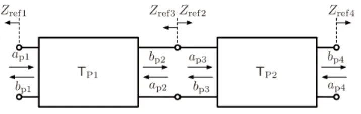
3.2 Cascading
Let us introduce the power-wave cascading matrix TP
(Fig. 13).
bp1
ap1
=TP
ap2
bp2
=
TP11 TP12
TP21 TP22
ap2
bp2
. (70) In terms of the elements ofSP,
TP= 1 SP21
SP12SP21−SP11SP22 SP11
−SP22 1
. (71)
We want bp1
ap1
=TP1
ap2
bp2
=TP1TP2
ap4
bp4
(72) to be valid. This requires thatbp2 =ap3andap2=bp3be sat- isfied at the interconnecting plane (Fig. 13). SinceV2 =V3 andI2 =−I3hold there,Zref2 =Z∗ref3follows from Eqs. (61) and (62) as a requirement[46]. This is in stark contrast with the ordinary T matrices, for whichZref2 =Zref3 is required.
So be extra careful when doing cascading operations with SPparameters or TPmatrices.
3.3 S Matrices of a Length of Transmission Line
The complex-referenced S matrix of a length,, of transmis- sion line is
S(Zref)= 1
Z02+Zref2 +2Z0Zrefcoth(γ)
×
Z02−Zref2 2Z0Zref/sinh(γ) 2Z0Zref/sinh(γ) Z02−Zref2
. (73)
WithZref=Z0, Eq. (73) reduces to
S(Z0) =
0 e−γ e−γ 0
, (74)
regardless of the value of . This property is used in the formulation of TRL[4],[21],[73]. It also is the reason for the line’s (generally unknown)Z0 becoming the reference impedance (Zref=Z0) of the new reference planes after per- forming TRL calibration.
More generally, a pair of reference impedancesZi1and Zi2 that makes S11 = S22 = 0 are known as the image impedances[78]of the 2-port. If
S(Zref1,Zref2) =
S11 S12
S21 S22
, (75)
then
S(Zi1,Zi2)=
0 e−θi12 e−θi21 0
, (76)
where θi21 andθi12 are the image propagation parameters.
Obviously,Zi1=Zi2=Z0andθi21=θi12 =γin the case of transmission lines.
The matrix elements of the complex-referenced SPma- trix of a length of transmission line are
SP11 (Zref1,Zref2)= (Z02−Zref1∗ Zref2) tanhγ+Z0(Zref2−Z∗ref1) (Z02+Zref1Zref2) tanhγ+Z0(Zref1+Zref2),
(77) SP22 (Zref1,Zref2)= (Z02−Zref1Zref2∗ ) tanhγ+Z0(Zref1−Z∗ref2)
(Z02+Zref1Zref2) tanhγ+Z0(Zref1+Zref2), (78) SP21 (Zref1,Zref2)=SP12 (Zref1,Zref2)
= 2Z0
(Zref1)(Zref2)/coshγ
(Z02+Zref1Zref2) tanhγ+Z0(Zref1+Zref2). (79) Note thatZref1 =Zref2=Z0doesn’t makeSP11 =SP22 =0.
In this sense, SPmatrices of lossy transmission lines are not terribly useful.
A pair of reference impedances that makes SP11 = SP22 = 0 is called the conjugate image impedances[55].
SP11 =SP22 =0 means that simultaneous conjugate match- ing is achieved at the input and output ports. Since a trans- mission line is a symmetric 2-port, the conjugate image impedances are the same for both ports. Unlike the image impedanceZ0, the conjugate image impedance depends on . This implies that it will be difficult to formulate VNA calibration algorithms based on power waves and to meas- ure SPparameters directly.
3.4 Amplifier Gains
The use ofSP11 (Zref), instead ofS11 (Zref), can be beneficial for reasons explained in§2.6. What about the use of 2-port SP
parameters? Suppose you are designing a multi-stage am- plifier. Consider a single stage within it (Fig. 14). Its 50-Ω- referenced power gain is|S21 (50Ω)|2. What is its power gain