INVITED PAPER
Special Section on Photonic Devices using Nanofabrication Technology and Their ApplicationsIntegration of Silicon Nano-Photonic Devices for Telecommunications
Seiichi ITABASHI†∗a), Hidetaka NISHI†, Tai TSUCHIZAWA†, Toshifumi WATANABE†, Hiroyuki SHINOJIMA†,Nonmembers, Rai KOU†,andKoji YAMADA†,Members
SUMMARY Monolithic integration of various kinds of optical compo- nents on a silicon wafer is the key to making silicon (Si) photonics practical technology. Applying silicon photonics to telecommunications further re- quires low insertion loss and polarization independence. We propose an integration concept for telecommunications based on Si and related mate- rials and demonstrate monolithic integration of passive and dynamic func- tional components. This article shows the great potential of Si photonics technology for telecommunications.
key words: siliconphotonics, integration, nanofabrication, telecommuni- cation
1. Introduction
Today’s advanced information society has reached its present state through the combination of large-capacity, high-speed communications networks for transmitting in- formation and electronic circuits for processing that infor- mation rapidly. If the advanced information society is to continue to expand, future telecommunications systems will need more broad bandwidth and more flexibility which en- ables network operation with low power consumption; in other words, high energy efficiency.
Current telecommunications systems are composed of separate optical components, such as optical fibers, wave- length filters, modulators, photodetectors (PDs), and lasers, and electronic control circuits. These components are made of various materials and manufactured individualy. They then have to be combined in certain configurations and installed. It is therefore very difficult to simultaneously achieve functionality, low power consumption and cost ef- fectiveness in a consistent manner. Si photonics technology is expected to solve these problems.
Optical components made of Si have many advantages, such as ultrasmall size, low cost, and convergence with elec- tronic devices. This is because Si technology is an industry standard that can provide low-cost, high-performance de- vices through high-density integration and mass-production techniques. The plan is to replace the various non-Si materi- als currently used to form optical devices with Si and related materials and to integrate them monolithically.
Various passive components based on Si nano-wire Manuscript received July 2, 2011.
Manuscript revised October 25, 2011.
†The authors are with NTT Microsystem Integration Laborato- ries, NTT Corporation, Atsugi-shi, 243-0198 Japan.
∗Presently, with NTT Advanced Technology Corporation.
a) E-mail: [email protected] DOI: 10.1587/transele.E95.C.199
waveguides (WGs) have already been developed [1], [2].
Dynamic components, such as Si-wire-based variable op- tical attenuators (VOAs) and germanium (Ge) PDs based on p-i-n structures, have also recently been demonstrated [3]. And now, researchers and engineers are finding ways to integrate those components while maintaining their perfor- mance.
In applying these integrated devices in telecommuni- cations systems, both low insertion loss and low polariza- tion dependence will be required. Integrating optical com- ponents while satisfying those requirements is the next im- portant challenge.
In this paper, we propose an integration concept suit- able for telecommunications and report the characteristics and applications of devices integrated based on the concept.
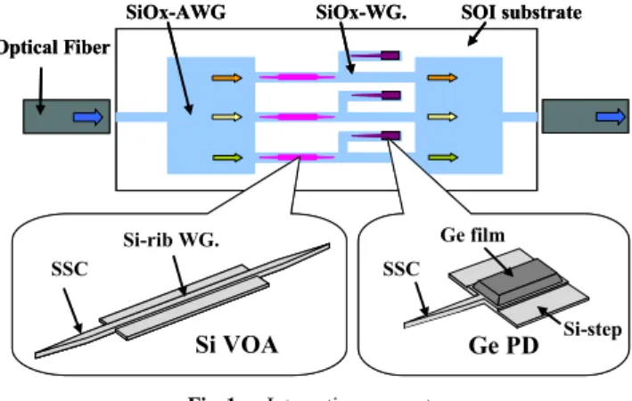
2. Integration Concept for Telecommunications Figure 1 shows our integration concept for telecommuni- cations based on Si and related materials, which have high affinity to Si.
Our idea is as follows. Passive functional components, such as WGs, branches and filters, are composed of Si- rich oxide (SiOx). Dynamic functional components, such as modulators and detectors, are made of Si or Ge. Because of the high affinity between these materials, it is possible to integrate all of the components monolithically on a SOI wafer.
Passive functional components made of silica (SiO2) are well known for their low propagation loss and low po- larization dependence. Components made of SiOxwould in-
Fig. 1 Integration concept.
Copyright c2012 The Institute of Electronics, Information and Communication Engineers
in SiOxWGs, enables us to obtain low insertion loss.
Long or bending Si nano-wire WGs tend to show polar- ization dependence. However, in our concept, the length of dynamic components is very small and their shape is very simple. These characteristics allows us to design and fab- ricate polarization-independent dynamic functional devices.
Finally, integrated devices with low loss and low polariza- tion dependence could be achieved and they would satisfy the requirements for telecommunications.
In the following sections, we describe our recent devel- opments in Si photonics technology based on this concept.
3. Integration with Low Insertion Loss
An issue in the integration of Si, Ge, and SiOxcomponents is thermal degradation. A silica WG is usually made at tem- peratures higher than 1000◦C [5], [6]. Si nanowire WGs are oxidized at such high temperatures, and electrical structures, such as the p-i-n junction, are destroyed during silica-WG fabrication. Therefore, we have to deposit SiOx films at a low temperature to realize the concept.
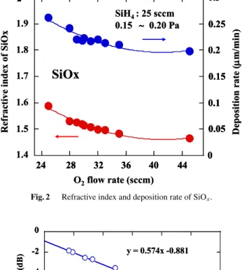
Our solution is electron cyclotron resonance (ECR) PECVD. SiOx films are deposited by ECR-PECVD with a mixture gas of SiH4 and O2. ECR plasma easily disso- ciates gas molecules and provides moderate energy to the substrate. This enables the fast deposition of high-quality film at temperatures lower than 200◦C [7].
Figure 2 shows the refractive index and deposition rate with changing O2flow rate. The SiH4flow rate was main- tained at 25 sccm. This experiment showed that the refrac- tive index of SiOxcan be controlled over a wide range from 1.47 to 1.60 simply by adjusting the flow rate of oxygen.
The deposition rate is high enough for the formation of the WG films with a thickness of a few micrometers. This re- sult indicates that SiOxby ECR-PECVD is a good silica film whose refractive index can be adjusted.
To evaluate the propagation loss, we made SiOxWGs with a refractive index contrast of 3%. The core is made of SiOx,whose refractive index is 1.515, and the overcladding is SiO2, whose refractive index is 1.47. These films were formed on 3-μm-thick thermal SiO2 on a Si wafer because the SiOx WGs are integrated with Si WGs on SOI wafer with 3-μm buried SiO2. Figure 3 shows an example of the transmittance results for SiOx WGs for the TE mode as a function of WG length. From the slope of the fitted line, we
Fig. 2 Refractive index and deposition rate of SiOx.
Fig. 3 Propagation loss of SiOx.
obtained propagation losses of 0.574 dB/cm. This value is low enough to make a practical device on a small chip.
Another issue is the large coupling loss between SiOx
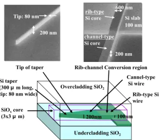
WGs and Si nanowire WGs, which results from the large difference in core size. Moreover, because the dynamic components, such as Si-VOAs with a p-i-n carrier injection structure, are based on a rib-type Si wire WG, we need an effective SSC for rib-type Si wire WGs to reduce the cou- pling loss. For channel-type Si wire WGs, a SSC consist- ing of a Si inverse taper and a low-index WG with a large core covering the taper has been developed [1], [8]. How- ever, it cannot be used in rib-type Si wire WGs because the Si taper core needs to be a channel-type one. Our solution was to modify the SSCs developed for channel-type WGs so that they could be used for rib-type ones. Figure 4 shows the structure of SSC for a Si rib-type WG. The Si WG is converted from a rib-type to a channel-type at the end and connected to a Si taper. The taper, which gradually becomes thinner toward the end, is 300-μm long and the tip is 80-nm wide. A SiOxWG covers the Si taper, which is formed by low-temperature deposition. The reflection due to the step between the rib and channel WGs does not, in fact, have
Fig. 4 Structure of SSC for Rib-type Si waveguide.
any effect on performance [9]. The coupling loss for one connection is 0.73 dB.
4. Integration with Low Polarization Dependence As described before, our integration concept requires dy- namic components with low polarization dependence. The typical dynamic component is the Si-VOA based on a rib- type wire WG, which has many advantages, such as a small footprint and fast response on the order of nanoseconds.
This type of the device almost always shows polariza- tion dependent loss (PDL) under operation without optimum design. We therefore have to make the PDL low.
The optimum design was done as follows. We ex- pressed the PDL as the difference in attenuation of TE and TM modes, |Att.TE −Att.TM|. The effective index of the TE and TM modes was calculated with a numerical mode solver. And, on the basis of the device simulation, we as- sumed that the distribution of carrier density is uniform in the core. We then determined the absorption coefficient to be constant. Therefore, we changed the value ofkTEandkTM by varying the parameters of the cross-section of the WG [Fig. 5(a)], i.e. rib height (h), rib width (w), and slab height (h2). The calculated PDL became lower than 1 dB when w was 360–500 nm, h was 300 nm, and h2was 40–80 nm.
Figure 5(b) shows an optical microscope image of a fabricated device consisting of a VOA, SSCs and a rib WG section. The lengths of the WG and the VOA are 6.3 mm and 1 mm, respectively.
First, we measured the optical transmission character- istics of the rib-type Si-wire WG at λ = 1530–1570 nm.
The propagation losses of TE and TM modes were 3.3 and 3.2 dB/cm, respectively. From these propagation losses, we estimated the PDL of the 6.3-mm-long Si WG to be less than 0.1 dB.
Next, we measured the optical transmission character- istics of the fabricated Si-VOA. Figure 6 shows the attenu- ation and PDL of a VOA with core width of 300 nm when
Fig. 5 Polarization independent VOA (a) Cross section of designed Rib-WG, (b) Optical microscope of Si-VOA.
Fig. 6 Attenuation and PDL of VOA.
forward bias is applied. The attenuation data are normalized by that at 0-mA injected current.
As injected current increased, the attenuation of both the TE and TM modes decreased, with a small difference.
We estimated the PDL of VOA operation to be 0.6 dB at 20- dB attenuation of the TE mode [10]. These results indicate that the PDL of dynamic functional device based on rib-WG can be suppressed low.
5. Integrated Devices and Applications in Tele-comm- unications Systems
Integrating those components while maintaining their per- formance is the next important challenge.
An integrated variable attenuator multiplexer/demulti- plexer (VMUX/DEMUX) is an important component for photonic networks, such as a reconfigurable opti- cal add/drop multiplexing (ROADM) system [4]. The VMUX/DEMUX consists of VOAs for optical power-level control, PDs for power-level monitoring, and an AWG for wavelength-division multiplexing (WDM). Silicon photon- ics technology has the potential to integrate those compo- nents on a single chip with low cost. Therefore, we have
bined by using SSCs.
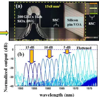
ECR-PECVD enables us to prevent thermal degrada- tion of Si WG and the p-i-n diode characteristics of the VOA during the SiOx deposition processes. As the ECR deposition method enables us to control the refractive index of SiOxup to 3%, the integrated device size is only about 15×8 mm2.
The fabricated SiOx-AWG enables wavelength demul- tiplexing of C-band signal in 16 channels with 200-GHz spacing. The crosstalk to the next channel is about−18 dB, which can be further reduced by modifying the design of the array-slab interface structure. The WG of the VOA is a rib-type one with a 600×200 nm core and 100-nm-thick slab. It has 1-mm-long p+and n+regions defined in the slab section. The doped regions are about 3μm apart. The propagated optical power is attenuated due to the carrier ab- sorption when the carriers are injected into the WG. The Si-VOA shows a response time as fast as a few nanoseconds and uniform attenuation over a wide wavelength range.
Owing to the Si-VOA, this device exhibited wavelength demultiplexing, and high-speed power-level adjustment in individual channels. Figure 7(b) shows the intensity adjust-
Fig. 7 Integrated Si-VOA and SiOx-AWG (a) Optical Image of Integrated device, (b) Intensity adjustment operation.
pendence. Then the integrated AWG-VOAs will satisfy the requirement.
5.2 AWG-PDs
As the second step, we integrated Ge-PDs with a SiOx- AWG.
Figure 8(a) shows an optical microscope image of the fabricated device. The Ge-PDs are buried in the SiOx-WG and are combined with the SiOx-AWG by using SSCs.
The Ge photodetector is 8×50μm in size. The 1-μm- thick Ge film was grown on a Si WG by a selective epitaxial
Fig. 8 Ge-PD and SiOx-AWG (a) Microscope image of AWG-PD (b) Spectra measured by buried PD.
process based on UHV-CVD [12]. The Ge detector has a low dark current of around 60 nA at−1 V, corresponding to dark current density of 15 mA/cm2. This low dark current means that the minimum detection power of our Ge pho- todetector is−41 dBm. We obtained responsivity of around 0.8 A/W. And these PDs show a response time as fast as a few gigahertz.
Figure 8(b) shows the first trial for receiving the light through AWGs and it’s detection by buried Ge-PDs. Good characteristics are achieved.
We believe that this device will be the key component of compact WDM equipment in future WDM access net- works.
5.3 VOA-PDs
The third step is the integration of dynamic functional com- ponents, Si-VOAs and Ge-PDs.
Here, we describe the monolithic integration of lateral p-i-n Si-VOAs with vertical p-i-n Ge-PDs.
When attempting to monolithically integrate a p-i-n type Si VOA and Ge PD, it is important that the fabrica- tion process for one device does not interfere with that of the other. An especially important factor for the design of the fabrication process is the thermal resistance of each de- vice. We therefore chose a process sequence that achieves monolithic integration of the Si VOA and Ge PD without adversely affecting either device [13], [14].
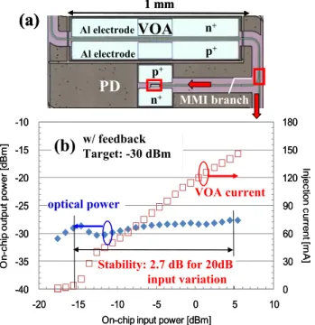
Figure 9(a) shows an image of a fabricated device. The device consists of a Si-VOA, MMI branch, and Ge PD, and SSCs at each end. The input light at 1560 nm is split by the MMI branch at the exit of the VOA and fed into a Ge
Fig. 9 VOA-PD (a) Microscope image of integrated device (b) Fast stabilization of transmitted light intensity.
detector on the chip and to an external fiber.
One of the most promising applications of an integrated VOA-PD, which equips low polarization dependence, is fast intensity equalization in a WDM transmission system with burst-mode packets, which usually have different pulse heights. A compact component integrating Si-VOAs and Ge PDs is beneficial for fast optical stabilization. To demon- strate the application, we attempted to equalize the optical intensity using the integrated VOA-PD device and an elec- tronic feedback circuit.
As shown in Fig. 9(b), the output power was stabilized within an error of 2.7 dB for a 20-dB variation of input power. In spite of a large dynamic range in the optical in- put, the feedback circuit works very stably. For example, the VOA injection current shows a stable and monotonic in- crease when the input optical power varies over a range of 20 dB. The 3-dB recovery time is about 100 ns, which would satisfy the timing criterion for burst optical packets in a 10- Gbps PON system [15]. Further optimization would reduce the recovery time to a few ten nanoseconds.
6. Conclusion
We have proposed an integration concept for telecommuni- cations. Based on the concept, various optical components can be integrated with low loss and low polarization depen- dence.
The performance of the integrated optical devices show sufficient potential for applying them in telecommunications area. We believe that developing this integration technology will be the key in realizing future network system.
Acknowledgments
The Ge film-growth process was carried out at the Wada Laboratory, University of Tokyo. We would like to thank all concerned for their assistance in this research. The authors would like to thank Prof. Kazumi Wada and Prof. Yasuhiko Ishikawa for their useful suggestions and discussions. And the authors also thank Dr. Hideaki Kimura and Dr. Takashi Yamada of NTT Access Network Service System Laborato- ries for their useful discussions about applications of silicon photonic devices in future telecommunications systems.
References
[1] T. Tsuchizawa, K. Yamada, H. Fukuda, T. Watanabe, J. Takahashi, M. Takahashi, T. Shoji, E. Tamechika, S. Itabashi, and H. Morita,
“Microphotonics devices based on silicon microfabrication technol- ogy,” IEEE J. Sel. Top. Quantum Electron., vol.11, no.1, pp.232–
240, 2005.
[2] W. Bogaerts, P. Dumon, D.V. Thourhout, D. Taillaert, P. Jaenen, J. Wouters, S. Beckx, V. Wiaux, and G.R. Baets, “Compact wavelength-selective functions in Silicon-on-Insulator photonic wires,” IEEE J. Sel. Top. Quantum Electron., vol.12, no.6, pp.1394–
1401, 2006.
[3] K. Yamada, T. Tsuchizawa, T. Watanabe, H. Fukuda, H. Shinojima, and S. Itabashi, “Application of Low-loss silicon photonic wire waveguides with carrier injection structure,” 4th Conference on
2002.
[9] T. Tsuchizawa, K. Yamada, T. Watanabe, H. Fukuda, H. Nishi, H.
Shinojima, and S. Itabashi, “Spot-size converters for Rib-Type sili- con photonic wire waveguides,” Proc. IEEE Intern. Conf. Group IV Photonics 2008, Torrent, 2008.
[10] H. Nishi, T. Tsuchizawa, T. Watanabe, H. Shinojima, K. Yamada, and S. Itabashi, “Compact and polarization-independent variable op- tical attenuator based on a silicon wire waveguide with a carrier injection structure,” Jpn. J. Appl. Phys., vol.49(04DG20), pp.1–5, 2010.
[11] M. Jinno, H. Kimura, Y. Hibino, K. Uehara, N. Kukutsu, F. Ito, and S. Matsuoka, “Towards ultrahigh-speed high-capacity networks,”
NTT Technical Review, vol.7, no.5, 2009.
[12] S. Park, Y. Ishikawa, T. Tsuchizawa, T. Watanabe, K. Yamada, S.
Itabashi, and K. Wada, “Effect of post-growth annealing on mor- phology of Ge mesa selectively grown on Si,” IEICE Trans. Elec- tron., vol.E91-C, no.2, pp.181–186, Feb. 2008.
[13] S. Park, K. Yamada, T. Tsuchizawa, T. Watanabe, H. Shinojima, H. Nishi, R. Kou, and S. Itabashi, “Influence of carrier lifetime on performance of silicon p-i-n variable optical attenuators fabricated on submicrometer rib waveguides,” Opt. Express, vol.18, no.11, pp.11282–11291, 2010.
[14] T. Tsuchizawa, K. Yamada, T. Watanabe, H. Shinojima, H. Nishi, and S. Itabashi, “Ultrasmall silicon photonic devices and integration technology toward Photonic-electronic convergence,” NTT Techni- cal Review, vol.8, 2010.
[15] S. Nishihara, M. Nakamura, K. Nishimura, K. Kishine, S. Kimura, and K. Kato, “10.3 Gbit/s burst-mode PIN-TIA module with high sensitivity, wide dynamic range and quick response,” Electron. Lett., vol.44, pp.222–223, 2008.
Seiichi Itabashi received the B.S. and M.S. degrees in physics from Tohoku Univer- sity, Sendai, Japan, in 1982 and 1984, respec- tively, and the Ph.D. degree from Hokkaido Uni- versity, Sapporo, Japan, in 1998. He is a Se- nior Research Engineer supervisor with NTT Microsystem Integration Laboratories, Atsugi, Japan. In NTT’s laboratories, he has been en- gaged in studies on X-ray and EUV optics. And he has engaged in research on silicon-based op- toelectronics devices. Currently, he is a Senior Engineer with NTT Advanced Technology Corporation. Dr. Itabashi is a Member of the Japan Society of Applied Physics.
tively, and the Ph.D. degree from the Univer- sity of Tokyo, Japan, in 1990. Currently, he is a Senior Research Engineer in NTT Microsys- tem Integration Laboratories, Atsugi, Japan. In NTT’s laboratories, he has engaged in studies on ECR plasma technology and its application to an etching process for microfabrication. His current research interest is fabrication technolo- gies for silicon based optoelectronics devices. Dr. Tsuchizawa is a Member of the Japan Society of Applied Physics.
Toshifumi Watanabe received the B.S. and M.S. degrees in applied physics from Tokyo In- stitute of Technology, Tokyo, Japan, in 1982 and 1984, respectively. Currently, he is a Senior Re- search Engineer with NTT Microsystem Inte- gration Laboratories, Atsugi, Japan. In NTT’s laboratories, he has engaged in layout process- ing studies for electron beam pattern writer and CAD data modulation for LSI and photonic cir- cuits. He is recently interested in robust algo- rithms of processing for very complex pattern layouts.
Hiroyuki Shinojima received the B.S. and M.S. degrees in applied physics from Tokyo In- stitute of Technology, Japan in 1984 and 1986, respectively, and the Ph.D. degree from Muro- ran Institute of Technology, Japan, in 2009. Cur- rently, he is a Senior Research Engineer in NTT Microsystem Integration Laboratories, Atsugi, Japan. In NTT’s laboratories, he has engaged in studies on material physics and nonlinear op- tics in semiconductor microcrystals. His current research interests include coherent control in sil- icon, material physics in low-dimensional semiconductors, and the origin of homochirality in terrestrial bioorganic compounds.
Rai Kou received the B.E. and M.E. de- grees in applied physics from Waseda Univer- sity, Tokyo, Japan, in 2007 and 2009, respec- tively. From 2007 to 2009, he was a visiting re- searcher at the National Institute for Materials Science (NIMS), Tsukuba, Japan, where he was engaged in the field of nonlinear optics and its related materials. In 2009, he joined the NTT Microsystem Integration Laboratories, Atsugi, Japan. His current research interests focus on integrated silicon photonic devices.
Koji Yamada received the B.E., M.E., and Ph.D. degrees in nuclear engineering from Kyushu University, Fukuoka, Japan, in 1986, 1988, and 2003, respectively. Currently, he is a Senior Research Engineer in NTT Microsystem Integration Laboratories. In NTT’s laboratories, He has been engaged in theoretical and exper- imental studies on beam dynamics in electron synchrotrons. Recently, he has been engaged in research on silicon-based nanophotonic struc- tures. Dr. Yamada is a Member of the Physical Society of Japan, the Japan Society of Applied Physics, the Atomic Energy Society of Japan, the Particle Accelerator Society of Japan.