Title Improvement for piezoelectric properties and domain structuresobservation of lead-based relaxor ferroelectric solid solutions( 本 文(Fulltext) )
Author(s) NUR HIDAYAH BINTI ZAINAL ABEDIN
Report No.(Doctoral Degree) 博士(工学) 甲第474号 Issue Date 2015-03-25 Type 博士論文 Version ETD URL http://hdl.handle.net/20.500.12099/51032 ※この資料の著作権は、各資料の著者・学協会・出版社等に帰属します。
2
GIFU UNIVERSITY
Improvement for piezoelectric properties and domain structures
observation of lead-based relaxor ferroelectric solid solutions
リラクサー強誘電体固溶体に於ける高効率圧電特性とドメイン構造観察
By
Nur Hidayah Binti Zainal Abedin
A Thesis Submitted to the Faculty of Graduate
Studies in Partial Fulfillment of the Requirements for the Degree
Doctor of Philosophy in Electronics and Information Systems
Engineering
Department of Electrical and Electronics Engineering
Gifu University, Japan
3
ACKNOWLEDGMENTS
This dissertation would not have been possible without the guidance and the help of several individuals who in one way or another contributed and extended their valuable assistance in the preparation and completion of this study.
First and foremost, I would like to express my sincere gratitude to my supervisors, Prof. Naohiko Yasuda and Associate Prof. Hidehiro Ohwa, whose expertise, understanding, and patience, added considerably to my graduate experience. I appreciate their vast knowledge and skills in many areas, their assistance in writing reports (i.e., grant proposals, scholarship applications and this thesis), guidance and support throughout my graduate program.
I would like to thank Prof. Osamu Sakurada from the Material Science and Technology Department for taking time out from his busy schedule to help and assistance my research project.
This work was supported in part by the Nippon Sheet Glass Foundation for Materials Science and Technology and Grant-in- Aid for Scientific Research (B) (No.16360150) from the Japan Society for the Promotion of Science.
I would also like to thank my family for the support they provided me through my entire life and in particular, words alone cannot express the thanks I owe to Muhammad Amiruddin, my husband and both my beautiful daughters, Nur Ariqa and Nur Arissa, without those love, encouragement and assistance, I would not have finished this thesis.
4
I wish to thank the other members of my committee for the motivation and assistance they provided at all levels of the research project. I am heartily thankful to my colleagues in Electrical and Electronics Engineering Departments and in particular, Natsumi Takahashi, Siti Faezah, Nor Liana, Shafika, Siti Khatijah, Nur Syazwana and Nor Faizah, my friends for moral support and help that enable me to complete this study.
I recognize that this research would not have been possible without the financial assistance of Majlis Amanah Rakyat (MARA) education loan scheme. I feel thankful to the staffs of Department of Electrical and Electronics Engineering, Gifu University, Japan.
My special thanks should be given to all Malaysian who helped me in many ways and cherish my life in Gifu University. Last but not the least, I offer my regards and blessings to all of those who supported me in any respect during the completion of the program.
Gifu, Japan Nur Hidayah Binti Zainal Abedin January 2015
5
CONTENTS
ACKNOWLEDGMENTS………..2 CONTENTS………....4 ACRONYMS………...6 LIST OF FIGURES………7 ABSTRACT………...12OBJECTIVE OF THIS STUDY……….…...15
1. INTRODUCTION………16
1.1 Piezoelectricity………..16
1.2 Ferroelectrics and Relaxor Ferroelectrics……….19
1.3 Perovskite Structure………...21
1.4 Crystal phases and spontaneous polarization orientation……….23
1.5 Morphotropic phase boundary………...24
1.6 PIN-PMN-PT……….26 1.7 PNN-PZT………...28 2. Experimental Procedure………...30 2.1 Preparation of samples………..30 2.1.1 24Pb(In1/2Nb1/2)O3-46Pb(Mg1/3Nb2/3)O3-30PbTiO3 single crystals………....30 2.1.2 0.5Pb(Ni1/3Nb2/3)O3-0.5Pb(Zr0.7Ti0.3)O3 ceramics……...32
2.2 Domain observation by Polarized Light Microscope (PLM)…………...33
2.3 Scanning Electron Microscopy (SEM)……….34
2.4 Piezoresponse Force Microscopy (PFM)………...36
3. Results and discussion………...42
3-1 Poling and depoling effects on dielectric properties and domain structures in relaxor 24Pb(In1/2Nb1/2)O3-46Pb(Mg1/3Nb2/3)O3-30PbTiO3 near a morphotropic phase boundary composition………..….42
3-1.1 Introduction………..42
3-1.2 Results and Discussion……….…....43
3-1.2.1 Complex relative permittivity εr………..…....43
3-1.2.2 P-E hysteresis loops………48
3-1.2.3 PLM images……….49
6
3-1.2.3.2 PLM images with poling………..52 3-1.2.4 SEM images………53 3-1.2.5 PFM images………56
3-2 Pressure-induced suppression of piezoelectric response in a 0.5Pb(Ni1/3Nb2/3)O3-0.5Pb(Zr0.7Ti0.3)O3 ceramic near a morphotropic phase
boundary………...61
3-2.1 Introduction………...61 3-2.2 Results and discussion………..62
3-3 Ferroelastic behavior in relaxor 24Pb(In1/2Nb1/2)O3-46Pb
(Mg1/3Nb2/3)O3-30PbTiO3 under shear stresses along [001] Direction…..72
4. Conclusion……….………...81 5. References………...84 List of publications………...91
7
ACRONYMS
FE Ferroelectric
RE Relaxor
AFE Antiferroelectric
AFM Atomic Force Microscopy
M Monoclinic
R Rhombohedral
T Tetragonal
O Orthorhombic
MPB Morphotropic Phase Boundary PLM Polarizing Light Microscopy PFM Piezoresponse Force Microscopy SEM Scanning Electron Microscopy
P Pressure
8
LIST OF FIGURES
Figure 1-1 Monocrystal and polycrystal polar axis……….18 Figure 1-2 Polarization of ceramic materials to generate piezoelectricity…...18 Figure 1-3 Example of piezoelectricity………19 Figure 1-4 Distinctive features between Ferroelectrics and relaxor ferroelectrics
in the temperature dependence of the complex relative permittivity…………...20
Figure 1-5 Structure of a perovskite of PbTiO3 with a chemical formula ABO3. The blue spheres are Pb2+, the red spheres are O2- and the green spheres are Ti4+. (a) paraelectric cubic phase above Curie temperature Tc; (b) ferroelectric tetragonal phase below curie temperature Tc………...22
Figure 1-6 Phases and crystal variants………....23 Figure 1-7 Difference spontaneous polarization orientation Ps in each crystal
phase of tetragonal, orthorhombic and rhombohedral phases……….24
Figure 1-8. Phase diagrams of (a) PZT, (b) PZN-PT and (c) PMN-PT [18]. (d)
The monoclinic MA phase rotating between the rhombohedral (R) and tetragonal (T) phases; (e) The monoclinic MC and orthorhombic (O) phases rotating in the (010) plane (shaded)……….25
Figure 1-9 Bridgman method………...26 Figure 1-10 P-E hysteresis loop at room temperature at 0.1 Hz for PIN-PMN-PT
and PMN-PT.………....27
Figure 1-11 PNN-PZT phase diagram……….28 Figure 1-12 Temperature dependence of the relative permittivityεr…………29
9
Figure 2-1 Phase diagram of PIN-PMN-PT ternary system and location of
24PIN-46PMN-30PT.……….………..31
Figure 2-2 Polarized Light Microscopy (Olympus BX51) Cutaway Diagram..34 Figure 2-3 Scanning Electron Microscopy’s diagram………35 Figure 2-4 Principle of electron microscope (SEM)………...35 Figure 2-5 Schematic illustration of a scanned tip AFM system. A flexible
cantilever with a tip at the end is rigidly connected with a xyz piezoelectric element. The optical lever consists of a laser diode beam that is focused on the back of the cantilever and bounces off reaching the photodetector.…………...37
Figure 2-6 Depiction of PFM operations. The sample deforms in response to the
applied voltage. This, in turn, causes the cantilever to deflect, which can then be measured and interpreted in terms of the piezoelectric properties of the sample.………..38
Figure 2-7 Sign dependence of the sample strain. When the domains have a
vertical polarization that is pointed downwards and a positive voltage is applied to the tip, the sample will locally expand. If the polarization is pointed up, the sample will locally contract. The phase of the measured response is thus proportional to the direction of the domain polarization.………39
Figure 2-8 Cantilever deflection change……….41 Figure 2-9 Vibration amplitude for parallel and anti-parallel orientation of
polarization………...39
Figure 3-1 Temperature dependence of the real part εr’ of complex relative permittivity εr along the [001]cub direction for (a) poled and (b) depoled 24PIN-46PMN-30PT single crystals for different frequencies on heating and cooling.……….46
10
Figure 3-2 Temperature dependence of the imaginary part εr” of complex relative permittivity εr along the [001]cub direction for (a) poled and (b) depoled 24PIN-46PMN-30PT single crystal for different frequencies on heating and cooling.……….47
Figure 3-3 Polarization P-Electric field E hysteresis loop along the [001]cub direction for 24PIN-46PMN-30PT single crystal at room temperature. The solid line indicates dP/dE at Ec.………48
Figure 3-4 Domain structures in a (001)cub plate of poled 24PIN-46PMN-30PT single crystal at T = (a) 50℃, (b) 125℃, (c) 145℃, (d) 155℃, (e) 180 ℃, and (f) of depoled one at 30℃.………....50
Figure 3-5 The domain structure in a (001)cub plate of 24PIN-46PMN-30PT single crystal along <110>cub directions with depoling.………...51
Figure 3-6 Domain structures in a (001)cub plate of 24PIN-46PMN-30PT single crystal (a) along <100>cub and (b) along <110>cub direction with poling.……...52
Figure 3-7 SEM surface images of depoled 24PIN-46PMN-30PT single crystal
on (001)cub surface etched chemically with aqueous solutions of HF(4.6wt%) and NH4F(36.4%), revealed at different areas ① and ② multiplied by (a) 10000, (b) 30000, and (c) 60000.………...………..55
Figure 3-8 Piezoresponse force microscopy images of depoled 24PIN-46PMN-
30PT single crystal on (001)cub surface.………...58
Figure 3-9(a)Planar view of piezoresponse image, (b)piezoresponse high Z vs tip
voltage V at point marked with + in (a), (c) piezoresponse high Z vs tip voltage V at higher tip voltage at the same point, (d) planar view of piezoresponse image at different areas, (e)piezoresponse high Z vs tip voltage V at point marked with + in (d), (f) piezoresponse high Z vs tip voltage V at higher tip voltage at the same point for 24PIN-46PMN-30PT single crystal on (001)cub surface. V multiplied by 10 for horizontal axis.………..60
11
Figure 3-10 X-ray diffraction pattern. The inset shows the structure sensitive
pattern around (2 00) diffraction line. ………...63
Figure 3-11 SEM surface images of poled 0.5PNN-0.5PZT(0.7/0.3) ceramics
etched chemically with aqueous solutions of a mixture of HF (4.6 wt %) and NH4F (36.4 wt %). ………...64
Figure 3-12 Resonance and antiresonance frequency characteristics of (a)
impedance and (b) phase for the poled 0.5PNN-0.5PZT(0.7/0.3) ceramics in the
k31 mode for various pressures.……….66
Figure 3-13 Temperature dependence of the relative permittivity εr and the loss tangent tanδ for poled 0.5PNN-0.5PZT(0.7/0.3) ceramics.………..68
Figure 3-14 Pressure dependences of (a) relative permittivity εr and (b) dielectric
loss tangent tan δ for poled 0.5PNN-0.5PZT(0.7/0.3) ceramics at 1 and 10kHz at
25 oC.……….69
Figure 3-15 P-E hysteresis loop at room temperature at 60Hz for
0.5PNN-0.5PZT(0.7/0.3) ceramics. ……….70
Figure 3-16 Optical micrograph of indentation with load of 0.2kgf made on
(001)cub plate in depoled 24PIN-46PMN-30PT single crystal………...77
Figure 3-17 Orthoscopy images on (001)cub plate of 24PIN-46PMN-30PT single crystal (a) with crossed Nicols parallel to [100]cub direction, (b) with sensitive color plate, (c) rotated by 45° around [001]cub direction, (d) multiplied (a) by 100 under indentation with load of 0.2kgf, and (e) under no shear stress. Α: 𝐹 = 0.2kgf, β: 𝐹 = 0.1kgf and γ: 𝐹 = 0.05kgf, and δ: distance between flower leaves pf optical strain images along [110] direction.……….78
12
Figure 3-18 Dependence of distance d between flower leaves of optical strain
images on applied force F.………79
Figure 3-19 Canoscopy images at location near flower leaf.………..80 Figure 3-20 SEM surface images of poled 24PIN-46PMN-30PT single crystal on
(001)cub surface etched chemically with aqueous solutions of HF(4.6wt%) and NH4F(36.4%), multiplied by 6000.………...80
Figure 3-21 Scheme of domain structure from tweed to twin induced by shear
13
Improvement for piezoelectric properties and domain structures
observation of lead-based relaxor ferroelectric solid solutions
Nur Hidayah Binti Zainal Abedin
ABSTRACT
The temperature dependence of the complex relative permittivity in a lead-based relaxor ferroelectric solid solution single-crystal 24Pb(In1/2Nb1/2)O3- 46Pb(Mg1/3Nb2/3)O3-30PbTiO3, abbreviated 24PIN-46PMN-30PT poled and depoled was measured from room temperature to 200℃ at various frequencies. The domain structures and dielectric properties of 24PIN-46PMN-30PT poled and depoled were studied by polarized light microscopy (PLM), piezoresponse force microscopy (PFM), scanning electron microscopy (SEM) and dielectric spectroscopy. The poled sample exhibits phase transitions from the ferroelectric (FE) phase to the relaxor (RE) phase on heating, and after that, the depoled one exhibits those from the RE phase to the glassy freezing on cooling. A RE-type dielectric dispersion with weak frequency (f) dependence was observed. Such a dielectric dispersions in RE state was found to be based on tweed domain structures observed by PLM and PFM due to the competition between antiferroelectric (AFE) and FE coupling in the RE state.
14
The temperature dependence of complex permittivity with resonance- and relaxor-type dielectric dispersions in the poled and depoled samples was characterized by hierarchical domain structures.
The ferroelastic behavior of 24PIN- 46PMN- 30PT was investigated under shear stresses using PLM and SEM. Optical strain patterns along the [110]cub directions from the orthoscope images under crossed Nicol, induced by shear stresses applied along the [001] direction, making use of a Vickers microindenter with a square-base diagonal line oriented along the {100}cub directions of the crystal were observed on its (001)cub plate for the first time. These patterns at a diagonal position reveal a flower-like pattern for ferroelastic transition from a square (S) lattice to a rectangular (R) lattice in a two-dimensional model system. Such ferroelastic behavior results from disorder-driven tweed domain structures based on the glassy freezing state in 24PIN-46PMN-30PT with depoling.
Electromechanical properties of 0.5Pb(Ni1/3Nb2/3)O3-0.5Pb(Zr0.7Ti0.3)O3 abbreviated (0.5PNN-0.5PZT(0.7/0.3)) ceramics near a morphotropic phase boundary (MPB) were investigated under the hydrostatic pressure p up to 600 MPa at room temperature, where the piezoelectric constants d33 = 850 pC/N and
d31 = 332 pC/N were obtained in this material. The remarkable change in the pressure dependence of the electromechanical response was found, where the resonance and antiresonance curves in impedance and phase in k31 mode for the transverse electromechanical property of 0.5PNN-0.5PZT(0.7/0.3) decrease with increasing pressure, and disappear completely at about p =600 MPa.
15
It was also confirmed that after removal of applied pressures, the electromechanical response recovers. Accompanied with such suppression of piezoelectric response, the increase in 30% of the permittivity εr with increasing
p, was observed.
Keywords: Relaxor PIN-PMN-PT single crystal, hierarchical domain structures,
PFM image, PLM image, SEM image, dielectric properties, poling and depoling, glassy freezing state, tweed structure, ferroelastic behavior, shear stress effect, orthoscope image, piezoelectricity, PZT, pressure effects, ferroelasticity
16
OBJECTIVE OF THIS STUDY
① Poling and depoling effects on dielectric properties and domain structures in relaxor ferroelectric solid solution single crystal near a morphotropic phase boundary composition.
② Domain structures from macroscopic to microscopic scale.
③ Domain structures and dielectric properties resulting from tweed precursors ④ Ferroelastic behavior under shear stresses along the [001] direction
⑤ Effect of pressure on the piezoelectric properties near a morphotropic phase boundary.
17
1. INTRODUCTION
1.1 Piezoelectricity
Piezoelectrics also called the piezoelectric effect are crystalline materials that exhibit an electromechanical coupling effect (interaction between the mechanical and the electrical state). The piezoelectric effect is a reversible process.The materials can exhibiting the direct piezoelectric effect (the internal generation of electrical charge resulting from an applied mechanical force) and also exhibit the reverse piezoelectric effect (the internal generation of a mechanical strain resulting from an applied electrical field).
The most common piezoelectric material is quartz. Certain ceramics, Rochelle salts, and various other solids also exhibit this effect .An example of man-made piezoelectric materials includes’ barium-titanate (BaTiO3), lead titanate (PbTiO3) and lead-zirconate–titanate (PZT).Piezoelectricity have many useful applications such as the production and detection of sound, generation of high voltages, electronic frequency generation, microbalances, to drive an ultrasonic nozzle, and ultrafine focusing of optical assemblies. Piezoelectricity also widely used in scientific instrumental techniques with atomic resolution, the scanning probe microscopies such as scanning tunneling microscopy (STM), atomic force microscopy (AFM), micro-thermal analysis (MTA), and scanning near-field optical microscopy (SNOM), and everyday uses such as acting as the ignition source for cigarette lighters and push-start propane barbecues. The word piezoelectricity comes from Greek and means “electricity by pressure” (piezo means pressure in Greek).
18
Piezoelectricity was discovered in 1880 by French physicists Jacques and Pierre Curie [1]. The converse effect was mathematically deduced from fundamental thermodynamic principles by Gabriel Lippmann in 1881 and then the existence was soon confirmed by the Curies. During World War II, a new class of synthetic materials, called ferroelectrics, which exhibited piezoelectric constants many times higher than natural materials was discovered by independent research groups in the United States, Russia, and Japan. From this discovery, barium titanate (BaTiO3), and later lead zirconate titanate (PZT) materials with specific properties for particular applications were develop.
Piezoelectricity is formed in crystals that have no center of symmetry. Figure 1-1 shows the monocrystal and polycrystal polar axis. Each molecule has a polarization, one end is more negatively charged and the other end is positively charged, and is called a dipole. This is a result of the atoms that make up the molecule and the way the molecules are shaped. The polar axis is an imaginary line that runs through the center of both charges on the molecule. In a monocrystal the polar axes of all of the dipoles lie in one direction. The crystal is said to be symmetrical because if you were to cut the crystal at any point, the resultant polar axes of the two pieces would lie in the same direction as the original. In a polycrystal, there are different regions within the material that have a different polar axis. It is asymmetrical because there is no point at which the crystal could be cut that would leave the two remaining pieces with the same resultant polar axis. In order to produce the piezoelectricity, the polycrystal is heated under the application of a strong electric field. The heat allows the molecules to move freely and the electric field forces all of the dipoles in the
19
crystal to line up and face in nearly the same direction as shown in Figure 1-2.
Figure 1-1 Monocrystal and polycrystal polar axis
Figure 1-2 Polarization of ceramic materials to generate piezoelectricity
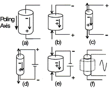
Figure 1-3 illustrates the piezoelectricity. Figure 1-3(a) shows the piezoelectric material without a stress or charge. If the material is compressed, then a voltage of the same polarity as the poling voltage will appear between the electrodes (figure 1-3(b)). If stretched, a voltage of opposite polarity will appear (figure 1-3(c)). Conversely, if a voltage is applied the material will deform. A voltage with the opposite polarity as the poling voltage will cause the material to expand, (figure 1-3(d))and a voltage with the same polarity will cause the material to compress (figure 1-3(e)). If an AC signal is applied then the material will vibrate at the same frequency as the signal (figure 1-3(f)).
20
Figure 1-3 Example of piezoelectricity
1.2 Ferroelectrics and Relaxor Ferroelectrics
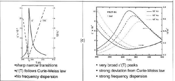
Relaxor ferroelectrics are a class of disordered crystals possessing peculiar structure and properties with either complex perovskite structure or bronze tungsten structure. As shown in Figure 1-4 the difference between normal ferroelectrics and relaxor ferroelectrics can be distinguished by three qualitatively different features in the temperature dependence of the complex relative permittivity. In normal ferroelectrics the real part of the complex relative permittivity, ε’ (T) shows a Curie-Weiss law behavior at the transition temperature Tc. While for the relaxor at the transition temperature the peak does have a divergence but it is broad and rounded. Such rounded peak position at Tm for relaxor, indicates the dynamic freezing temperature or glass like transition [26].Then,there is a strong frequency dependence in the peak position, Tm ofε’ (T). Lastly, the polarization in normal ferroelectric goes to zero at Tc.
21
While in the relaxor the polarization extends well beyond Tm [25]. The fact that there is zero polarization at Tc shows that polar nanodomains vanish whereas in the relaxor the nanodomains persist well beyond the glassy transition temperature [1].
Figure 1-4 Distinctive features between Ferroelectrics and relaxor ferroelectrics
22
1.3 Perovskite Structure
Most of the relaxor ferroelectric materials such as Pb(Mg1/3Nb2/3)O3, Pb(Sc1/2Ta1/2)O3, and Pb(In1/2Nb1/2)O3 have a perovskite crystal structure. A perovskite structure is any material with the same type of crystal structure as calcium titanium oxide (CaTiO3), known as the perovskite structure, with the oxygen O ions at the face centers.
The general chemical formula for perovskite compounds is ABX3, where 'A' and 'B' are two cations of very different sizes, and X is an anion that bonds to both. The 'A' atoms are larger than the 'B' atoms. The ideal cubic-symmetry structure has the B cation in 6-fold coordination, surrounded by an octahedron of anions, and the A cation in 12-fold cuboctahedral coordination. The relative ion size requirements for stability of the cubic structure are quite stringent, so slight buckling and distortion can produce several lower-symmetry distorted versions, in which the coordination numbers of A cations, B cations or both are reduced.
The perovskite structure is adopted by many oxides that have the chemical formula ABO3. In the idealized cubic unit cell of such a compound, type 'A' atom sits at cube corner positions (0, 0, 0), type 'B' atom sits at body centre position (1/2, 1/2, 1/2) and oxygen atoms sit at face centred positions (1/2, 1/2, 0).
The relative ion size requirements for stability of the cubic structure are quite stringent, so slight buckling and distortion can produce several lower-symmetry distorted versions, in which the coordination numbers of A cations, B cations or both are reduced. Tilting of the BO6 octahedra reduces the coordination of an undersized A cation from 12 to as low as 8. Conversely,
23
off-centering of an undersized B cation within its octahedron allows it to attain a stable bonding pattern. The resulting electric dipole is responsible for the property of ferroelectricity and shown by perovskites such as BaTiO3 that distort in this fashion. The orthorhombic and tetragonal phases are most common non-cubic variants.
Complex perovskite structures contain two different B-site cations. This results in the possibility of ordered and disordered variants.
Figure 1-5 Structure of a perovskite of PbTiO3 with a chemical formula ABO3. The blue spheres are Pb2+, the red spheres are O2- and the green spheres are Ti4+. (a) paraelectric cubic phase above Curie temperature Tc; (b) ferroelectric tetragonal phase below curie temperature Tc.
24
1.4 Crystal phases and spontaneous polarization orientation
A ternary PIN-PMN-PT solid solution was known to be a relaxor ferroelectrics with perovskite structure. Phase transition in crystal involves the polarization rotation, dipole and vector directions. Figure 1-6 shows the phases and crystal variants of the cubic, pseudo-cubic, tetragonal, rhombohedral, orthorhombic and monoclinic phases. Figure 1-7 shows the difference spontaneous polarization orientation in each crystal phase. Tetragonal phase has 6 equivalent spontaneous polarization Ps in [100] direction. While for rhombohedral phase and orthorhombic phase, has 8 and 12 variants of spontaneous polarization Ps in [111] direction and [110] direction, respectively.
Figure 1-6 Phases and crystal variants.
25
Figure 1-7 Difference spontaneous polarization orientation Ps in each crystal
phase of tetragonal, orthorhombic and rhombohedral phases.
1.5 Morphotropic phase boundary
In the vicinity of the morphotropic phase boundary (MPB), certain perovskite-type relaxor ferroelectrics show excellent properties such as large dielectric response and high electromechanical coupling constant. Such superior piezoelectric properties materials are importance for applications such as electrostrictive actuators and sensors, because of the large dielectric and piezoelectric constants. The term “morphotropic” was originally referred to phase transitions due to changes in composition (59). Nowadays, the term ‘morphotropic phase boundaries’ (MPB) is used to refer to the phase transition between the tetragonal and the rhombohedral ferroelectric phases as a result of varying the composition or induced by pressure (17,59,78,).
In the MPB, the crystal structure changes abruptly and electromechanical properties in piezoelectric materials are maximum. As a result, the common piezoelectric materials used for MPB applications are usually complex, engineered, structured solid solutions, which lead to a complicated manufacture
26
as well as complexity of the microscopic origins study of their properties. Example of complex-structured and require a complicated and costly process to prepare its solid solutions is lead zirconate titanate - PbZr1−x Ti x O3 (PZT) which is a perovskite ferroelectrics that has a MPB between the tetragonal and rhombohedral FE phases in the temperature-composition phase diagram. Furthermore, the study of the microscopic origin of PZT properties is very complicated. Figure 1-7 shows the phase diagrams of PZT, PZN-xPT and PMN-xPT around the MPB [18] as an example which involves the rhombohedral, tetragonal orthorhombic and monoclinic phases. Recently both the orthorhombic phase and monoclinic phase have been observed for PZN-xPT and PMN-xPT single crystals [89-93]..
Figure 1-7. Phase diagrams of (a) PZT, (b) PZN-PT and (c) PMN-PT [18]. (d)
The monoclinic MA phase rotating between the rhombohedral (R) and tetragonal (T) phases; (e) The monoclinic MC and orthorhombic (O) phases rotating in the (010) plane (shaded).
27
1.6 PIN-PMN-PT
Pb(In1/2Nb1/2)O3-Pb(Mg1/3Nb2/3)O3-PbTiO3 (PIN-PMN-PT) single crystals were grown with a modified Bridgman method, where it is a method of growing single crystal ingots or boules. It is a popular method of producing certain semiconductor crystals, such as gallium arsenide and many more. It involves heating polycrystalline material in a container above its melting point and slowly cooling it from one end where a seed crystal is located. Single crystal material is progressively formed along the length of the container. The process can be carried out either in horizontal or vertical geometry.
28
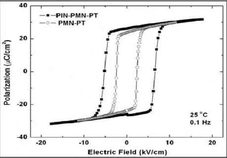
Figure 1-6 P-E hysteresis loop at room temperature at 0.1 Hz for PIN-PMN-PT
and PMN-PT.
PIN-PMN-PT is reported to have ferroelectric properties as shown in Figure 1-6. The coercive electrical field of PIN–PMN–PT crystals was found to be 6kV/cm, higher than PMN–PT crystal’s coercive electrical field, thus a higher electric field or voltage can be applied to the PIN-PMN-PT transducers. More importantly, the reliability is also improved because the transducers are capable of handling higher voltages. Compared to PMN-PT, the thermal stability of PIN– PMN–PT crystal seems to be better. The transition temperature TR/T and Curie temperature TC of PIN-PMN-PT single crystal, which denote the temperature limits for piezoelectric crystal applications, are increased to 117°C and 160°C. Therefore, PIN-PMN-PT transducers can be used at a higher temperature than PMN-PT.
29
1.4 PNN-PZT
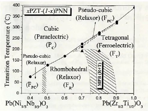
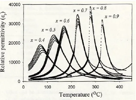
Pb(Ni1/3Nb2/3)O3, Lead Nickel Niobate (abbreviation PNN) is a well-known lead-based complex perovskite compound and as well as PMN, it’s exhibit a maximum dielectric constant at about -150℃. Improvement of the piezoelectric characteristics due to increase of dielectric constant at room temperature, by adding the PNN to PZT ceramics, the sintering temperature is reduce and also decrease the coercive field. Figure 1-7 shows a phase diagram and figure 1-8 shows the temperature dependence of the relative permittivityεr, respectively.
30
31
2. Experimental Procedure
2.1 Preparation of samples
2.1.1 24Pb(In1/2Nb1/2)O3-46Pb(Mg1/3Nb2/3)O3-30PbTiO3 single crystals
Ternary PIN-PMN-PT solid solution single crystals were grown by the Bridgman technique using [011]cub -oriented seed crystals [2]. The concentrations of PIN, PMN, and PT in the solid solution single crystal PIN-PMN-PT plate used in this work were determined [3] to be 24, 46 and 30, respectively, by inductive charge plasma (ICP) analysis. The grown 24PIN-46PMN-30PT crystal [4-8] was located on the rhombohedral phase side near the MPB composition in the narrow region between MPBs of 68PMN-32PT and 63PIN-37PT binary systems in a phase diagram of a ternary system, as shown in Figure 2-1. The crystals were cut into plates with (001)cub orientation, confirmed by X-ray diffraction and from Laue photographs. Both surfaces were polished to optical quality using diamond paste with the final particle size of 0.1μm. The domain structures were analyzed by polarizing light microscopy (PLM; BX51, Olympus Corp., Tokyo, Japan). Piezoelectric force microscopy (PFM) studies were performed using a commercial PFM device (SPA300/SPI3800N, Seiko Inc., Tokyo, Japan) [9]. The electrical capacitance and dielectric loss tangent tan δ were measured using an inductance, capacitance, resistance LCR meter (HP-4154A, Agilent Technologies, Santa Clara, CA) at 1, 5, 10, 50 and 100 kHz with the probe field lower than 10 V/cm at a rate of 1 K/min. The relationship between polarization and electric fields was examined with Sawyer-Tower circuit. The specimens were poled at 8 kV/cm at room temperature in an insulating liquid, silicone oil, to prevent arcing.
32
The polished specimens were chemically etched at room temperature with an aqueous solution of a mixture of HF (4.6 wt %) and NH4F (36.4 wt %) to make the domain structures visible [10]. The etched surfaces without conductive coating were probed using a commercial scanning electron microscope (SEM; S-4300 type G, Hitachi Ltd., Tokyo, Japan) at a magnification of 6x10³ and an acceleration voltage of 5 kV [10]. The Vickers microhardness Hv was measured [11] at room temperature by the indentation method (HM-101, AVK-CO, Mitutoyo Co. Ltd.). The diamond indenter used is a square-base micro-Vickers pyramid with a nominal angle of 68.0° between the face and the vertical axis. The crystal was set on the specimen stage of the apparatus to keep the (001) crystal face perpendicular to the indenter. The indenter with loads was pulled at a velocity of 0.01 mm/s down to the crystal surface at room temperature. The contact period of the indentation with the surface was 15s. The indentations were observed by using an optical microscopy (OM). Hv was determined with the equation: 1.854(F/d2), where F (kgf) and d (mm) are load and length of the diagonal of the indentation, respectively.
Figure 2-1 Phase diagram of PIN-PMN-PT ternary system and location of
33
2.1.2 0.5Pb(Ni1/3Nb2/3)O3-0.5Pb(Zr0.7Ti0.3)O3 ceramics
0.5PNN-0.5PZT(0.7/0.3) ceramics were prepared using the columbite precursor method [12,13 ]. The rectangular plate specimen with dimensions of 3.1w×12.6l×0.46t mm3 was prepared for the measurement of the k31 mode. Electrical capacitance and the dielectric loss tangent tanδ were measured using an inductance, capacitance, resistance LCR meter (HP-4154A) at 1, 10 and 100 kHz at 1 V/cm. The specimens were poled in a 10 kV/cm electric field while cooling from well above the transition temperature to 25oC in an insulating liquid, i.e., silicone, to prevent arc discharge. The relationship between polarization (P) and electric field (E) was examined with an ordinary Sawyer-Tower circuits at room temperature at 60Hz.
The electromechanical coupling factors k were measured by the resonance and antiresonance frequency method using an impedance gain phase analyzer (HP-4194A; network mode) [14]. The piezoelectric constant d33 was measured using a d33 meter (Model ZJ-3B/4B). The pressure apparatus used to apply hydrostatic pressure to samples was described elsewhere [15,16].
The polished samples were chemically etched at room temperature with an aqueous solution of a mixture of HF (4.6 wt %) and NH4F (36.4 wt %) to make the domain structures visible [10]. The etched surfaces were probed using a commercial scanning electron microscope (Hitachi type G S-4300) at magnifications of 5x10³ and 60x103 and an acceleration voltage of 5 kV.
34
2.2 Domain observation by Polarized Light Microscope (PLM)
By using the Polarized Light Microscopy (OLYMPUS: BX51) in crossed polarization state the domain structures were observed. A polarizing microscope has a pair of polarizing devices in the optical train. The first polar (polarizer) defines the initial plane of polarization for light entering the microscope and is located between the illuminator and the condenser. The other polar (analyzer) is usually placed between the objective and the ocular tube and defines the plane of polarization of the light reaching the ocular. One or both must be accurately rotatable about the optical axis of the instrument.
Crossed polarization state
In Figure 2-2, polarizer 1 is oriented vertically to the incident beam so it will pass only the waves that are vertical in the incident beam. The wave passing through polarizer 1 is subsequently blocked by polarizer 2 because the second polarizer is oriented horizontally with respect to the electric field vector in the light wave. The concept of using two polarizes oriented at right angles with respect to each other is commonly termed crossed polarization and is fundamental to the practice of polarized light microscopy.
The brightest visible was used as 0°and from there the stage sample was rotated 45°in counter clockwise. The observation was done at magnification of 1.25 times, 10 times and 40 times of objective lens.
35
Figure 2-2 Polarized Light Microscopy (Olympus BX51) Cutaway Diagram
2.3 Scanning Electron Microscopy (SEM)
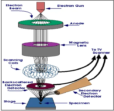
A scanning electron microscopy (SEM) is a type of electron microscope that images a sample by scanning it with a high-energy beam of electrons in a raster scan pattern. The electrons interact with the atoms that make up the sample producing signals that contain information about the sample’s surface topography, composition, and other properties such as electrical conductivity.
The SEM is an instrument that produces a largely magnified image by using electrons instead of light to form an image. A beam of electrons is produced at the top of the microscope by an electron gun. The electron beam follows a vertical path through the microscope, which is held within a vacuum. The beam travels through electromagnetic fields and lenses, which focus the beam down toward the sample. Once the beam hits the sample, electrons and X-rays are ejected from the sample. Detectors collect these X-rays, backscattered
36
electrons, and secondary electrons and convert them into a signal that is sent to a screen similar to a television screen. This produces the final image.
Figure 2-3 Scanning Electron Microscopy’s diagram
37
2.4 Piezoresponse Force Microscopy (PFM)
The polished samples were attached on a copper plate with silver paste (DuPont silver paste: 4922N). PFM studies were performed using the Scanning probe microscope system (SPI3800N, Seiko Instruments Inc).The Microscope unit and software measurement was SPA300V and SPIWin.
An external voltage was applied to the crystal surface through the Al coated cantilever (SI: DF3-R, f=27 kHz, C=1.6N/m) with a tip apex radius of~10nm as a top electrode for the 24PIN-46PMN-30PT single crystals. For the NBT-BT single crystals, an external voltage was applied to the crystal surface through the Al coated cantilever (SI; DF3-R, f=25 kHz, C=1.4N) with a tip apex radius of 30 nm as a top electrode. While the other surface that been attached on the copper plate with silver paste as a bottom electrode.
The PFM images were taken over 20µm, 3µm and 300nm scans at room temperature (RT). Begin with 5V and ending with 30V in increments of 5V the AC voltage was applied between the tip top electrode and the bottom one of the sample for the each of the length scales. The displacement direction of cantilever deflection sensitivity was automatically set for each measurement and the acquisition of the voltage gain (signal ratio) was set 10 times. In addition, the obtained Acos images of samples were analyzed for surface roughness analysis and Z/V curves were measured.
Principles of PFM
Piezoresponse force microscopy (PFM) is a variant of atomic force microscopy (AFM) that allows imaging and manipulation of ferroelectricdomains.
38
Figure 2-5 Schematic illustration of a scanned tip AFM system. A flexible
cantilever with a tip at the end is rigidly connected with a xyz piezoelectric element. The optical lever consists of a laser diode beam that is focused on the back of the cantilever and bounces off reaching the photodetector.
In PFM operation, a conductive AFM tip is brought into contact with the surface of the studied ferroelectric or piezoelectric materials, and a pre-set voltage is applied between the sample surface and the AFM tip, establishing an external electric field within the sample. Due to the electrostriction, or "inversed piezoelectric" effects of such ferroelectric or piezoelectric materials, the sample would locally expand or contract according to the electric field as shown in Figure 2-6.
39
Figure 2-6 Depiction of PFM operations. The sample deforms in response to the
applied voltage. This, in turn, causes the cantilever to deflect, which can then be measured and interpreted in terms of the piezoelectric properties of the sample.
As mentioned above, the direction of sample polarization determines the sign of the response. Figure 2-7 demonstrates this idea. For example, if the initial polarization of the electrical domain of the measured sample is perpendicular to the sample surface, and parallel to the applied electric field, the domains would experience a vertical expansion.
Since the AFM tip is in contact with the sample surface, such domain expansion would bend the AFM cantilever upwards, and result in an increased deflection compared to the status before applying the electric field. Conversely, if the initial domain polarization is anti-parallel to the applied electric field, the domain would contract and in turn result in a decreased cantilever deflection (Figure 2-8). The amount of cantilever deflection change, in such situation, is directly related to the amount of expansion or contraction of the sample electric domains, and hence proportional to the applied electric field.
40
Figure 2-7 Sign dependence of the sample strain. When the domains have a
vertical polarization that is pointed downwards and a positive voltage is applied to the tip, the sample will locally expand. If the polarization is pointed up, the sample will locally contract. The phase of the measured response is thus proportional to the direction of the domain polarization.
41
If the applied voltage contains a small AC component, the inversed piezoelectric response from the sample would result in sample surface oscillation in the same frequency as the applied AC voltage.
In the case that the sample is an ideal piezoelectric crystal, its polarization 𝑃⃗ would be related to applied mechanical stress 𝑆 by the following equation:
Pi = dijkSjk in which dijk is the rank-3 piezoelectric tensor of the material. For such materials with tetragonal crystal structures, this piezoelectric tensor can be reduced to the following form:
in which case, under the applied AC modulation voltage V = V0cos(ωt), sample surface vibration would take the form ΔZ = ΔZ0cos(ωt + φ), with the vibration amplitude ΔZ0 = d33V0, and phase f = 0 if the sample domain polarization is oriented parallel to the applied electric field, and out of φ = 180° if it is oriented anti-parallel to the applied electric field (Figure 2-7). Such oscillation would be directly reflected in the amplitude and phase signal of the AFM probe contacting the surface, and can be read out using a lock-in amplifier.
42
Figure 2-7 Vibration amplitude for parallel and anti-parallel orientation of
polarization
Z/V curve measurement
Z / V curve showing the relationship between the applied bias voltage and
distance (Z) of the AFM tip and sample. Using the Acos image that been scan 300nm scale with 30V applied AC voltage, start with -2V and ending with 2V on the chosen point the AC bias was applied at 100msec. Then with the same condition the measurement continue for (-8V, 8V), (-10V, 10V), (-20V, 20V), (-30V, 30V), (-40V, 40V), (-50V, 50V), (-60V, 60V), (-70V, 70V), (-80V, 80V), (-90V, 90V) and (-100V, 100V) of AC bias.
43
3. Results and discussion
3-1
Poling and depoling effects on dielectric properties and domain
structures in relaxor 24Pb(In1/2Nb1/2)O3-46Pb(Mg1/3Nb2/3)O3-30PbTiO3
near a morphotropic phase boundary composition
3-1.1 Introduction
In relaxor ferroelectric solid solutions exhibiting superior piezoelectric properties [19-22], the domain structure used to accommodate strains has been reported[5,23-26] to be due to the tweed structure based on the competition between antiferroelectric (AFE) and ferroelectric (FE) interactions. Many kinds of relaxor such as Pb(Mg1/3Nb2/3)O3(PMN)[27], Pb(Sc1/2Ta1/2)O3(PST) [28], and Pb(In1/2Nb1/2)O3(PIN) [29] were known. In the vicinity of morphotropic phase boundary (MPB), from rhombohedral to tetragonal through a monoclinic or orthorhombic phase polarization rotation model have been [21,22,30-33]reported for superior piezoelectric properties. Recently a new type of ternary PIN-PMN-PbTiO3(PT) crystal with some advantages has attracted much attention for piezoelectric applications [5-7,34 ]. One of the key advantages of a ternary PIN-PMN-PT crystal over binary PMN-PT is the higher coercivity Ec [7,34]. The Ec of the PIN-PMN-PT crystal was about 6kV/cm, about 2 times more than that of the PMN-PT crystal. Moreover, PIN-PMN-PT crystal was reported [7,34 ] to have improved linear strain response over a large field range. Thus, such improvements expand the operating conditions for crystal-based transducers [6,7,34]. The ordered PIN [29], PMN [35] and PbTiO3(PT) [36] formed as each element for PIN-PMN-PT solid solutions were reported to be
44
AFE, relaxor (RE) and FE, respectively. Relaxor ferroelectrics showing superior piezoelectric properties was known [35,37,38] to be associated with the mechanism that accommodates the strain energy through the difference in local volume ΔV with disordering. In this paper, the dielectric properties such as complex permittivity, polarization and the change in domain structures with poling and depoling are presented and discussed based on the tweed and twin domain structures in relaxor state in ternary relaxor PIN-PM-NPT.
3-1.2 Results and Discussion
3-1.2.1 Complex relative permittivity ε
rFigures 3-1 (a) and (b) and 3-2 (a) and (b) show the temperature dependence of the real part εr’ and the imaginary part εr” of the complex relative permittivity εr for the poled and depoled 24PIN-46PMN-30PT (001)cub plates, respectively. A remarkable difference in εr between the poled and depoled 24PIN-46PMN-30PT crystal can be observed in Figures 3-1 and 3-2. Such changes were found to be associated with the changes in phase transitions between the FE to RE phase for poled sample and the RE to glassy phase for the depoled sample.
For the poled sample, the εr’ and εr” anomalies were found at T1, T2, and
T3 and then at Tm for εr’ and at Tm’ for εr”. On heating, their values increased with increasing frequency (f), indicating a resonance type dispersion at temperatures (T) up to T1=123.1℃, the decrease, and then reveal a shoulder-like increase up to
45
On further heating, their values revealed a relaxor-type dispersion characterized by the broad maximum at Tm with a decrease for εr’ value and an increase in εr” value at the inflection point Tm’ =152.0℃ with increasing f in the RE phase above T3 and furthermore at higher temperatures far away from Tm and
Tm’, another dielectric dispersion characterized by the decrease in magnitude of εr” with f was observed. The difference in dielectric dispersions between the increase with f and the decrease with f above T3 may be associated with the local formation and annihilation of a polar nanoregion in the RE phase.
On the cooling run for the depoled sample, the dielectric dispersion characterized by the decrease in εr” with f was observed. On further cooling, the broad maximum of εr” at Tm” with the increase in its value with f and with a weak
f dependence of Tm” in the RE phase was observed and the glassy freezing behavior was observed as an inflection point at Tf [27] which is almost f- independence. In this case, Tm” is almost independent of f. Such a weak frequency dependence of Tm” indicates that the freezing temperature Tf is close to
Tm”. These remarkable characteristics for the glassy freezing behavior in the PIN-PMN-PT sample were compared with those of the typical PMN-PT sample with a strong f dependence of Tm [27,39-41].
The tan δ of depoled sample tended to saturate with small fluctuations on cooling for each frequency. Its saturated value was estimated to be 0.051 and 0.037 at 100kHz and 1kHz, respectively. On the other hand, for the poled sample, tan δ was estimated to be 0.0110 and 0.0006 at 100 kHz and 1 kHz, respectively.
46
The difference Δ tan δ in tan δ with poling was estimated to be about 0.04. This value was compared with 0.1 for PMN-PT reported previously [27,39,40]. Such difference in tan δ with poling was reported [32,35,38-40,42] to be related to the energy loss associated with the volume difference with disordering in relaxor ferroelectric solid solutions. On the other hand, the dielectric loss tan δ was pointed out [27,39] to be essentially the isotemporal cross section of the distribution function G(τ) of relaxation time τ. A sharp step in G(τ) was found near Tm, whose step did not shift to higher temperatures with increasing f in contrast to that in the case of PMN reported previously [27,39].
47
Figure 3-1 Temperature dependence of the real part εr’ of complex relative permittivity εr along the [001]cub direction for (a) poled and (b) depoled 24PIN-46PMN-30PT single crystals for different frequencies on heating and cooling.
48
Figure 3-2 Temperature dependence of the imaginary part εr” of complex relative permittivity εr along the [001]cub direction for (a) poled and (b) depoled 24PIN-46PMN-30PT single crystal for different frequencies on heating and cooling.
49
3-1.2.2 P-E hysteresis loops
The P-E hysteresis loop was observed at room temperature as shown in Figure 3-3. The remanent polarization Pr and coercive field Ec were estimated to be 24μC/cm2 and 5.7kV/cm, respectively, compared with 25μC/cm2 and 5.5 kV/cm reported[7,34] previously. The coercive field Ec of the sample is 2 times larger than that of binary PMN-PT (2kV/cm) [7,34]. The asymmetry in the shape of P-E hysteresis curve around the coercive field Ec with its derivative of dP/dE with a smaller value above Ec was found in Figure 3-3. Such phenomena may be due to the electric field-induced forced transition.
Figure 3-3 Polarization P-Electric field E hysteresis loop along the [001]cub direction for 24PIN-46PMN-30PT single crystal at room temperature. The solid line indicates dP/dE at Ec.
50
3-1.2.3 PLM images
The PLM images obtained with heating and cooling runs in the poled and depoled sample are shown in Figure 3-4. The remarkable changes in PLM images between poled and depoled samples were found in Figure 3-4. In the FE phase characterized by the piezoelectric resonance-type dielectric dispersion, the orthorhombic domain pattern with 90° walls parallel to the {001}cub planes [33,43,44] is shown in Figure 3-4(a), then that with 60° walls parallel to the {011}cub planes [44] in Figure 3-4(b), then tetragonal broader domains in Figure 3-4(c), then smaller domains with nanopolar region in the RE phase [45] characterized by the relaxor type dielectric dispersionin Figure 3-4(d), and then much smaller domains in the phase characterized by the dielectric dispersion with the decrease in ε” with f in Figure 3-4(e) on heating run. Subsequently, on cooling run, the domain structure in the glassy freezing state, which is oriented randomly with Gaussian distribution [5,40] in RE phase is shown in Figure 3-4(f) below Tf. The remarkable change in εr with depoling and poling is considered to be due to the change in domain structures. The larger εr in the RE phase is related to the tweed domain structures (Figure 3-4(f)), whereas the reduced εr in the FE phase is related to the orthorhombic domain structures with the ordered orientations for the FE phase transitions (Figure 3-4(a), (b), (c)).
51
(a)T=50℃
(b)T=125℃
(c)T=145℃
(d)T=155℃
(e)T=180℃
(f)T=30℃
Figure 3-4 Domain structures in a (001)cub plate of poled 24PIN-46PMN-30PT single crystal at T = (a) 50℃, (b) 125℃, (c) 145℃, (d) 155℃, (e) 180 ℃, and (f) of depoled one at 30℃.
<010>
<
10
52 3-1.2.3.1 PLM images with depoling
The domain structure in the depoled 24PIN-46PMN-30PT (001)cub plate [5] shows small spindle-like morphology [24,33] with the domain strips having wavy and blurred margin or walls with a width of few 3-7μm or less, forming labyrinth structures on the (001)cub plate in the 24PIN-46PMN-30PT single crystal as shown in Figure 3-5, when observed with crossed polarizers parallel to the <100>cub direction. Such optical domains exhibit the extinction along <110>cub directions. The domains belong to the rhombohedral phase with spontaneous polarization along the <111>cub direction [24,33]. These domains are 71° or 109° macrodomains. The domain structure in the nonergodic relaxor (NR) state [40] is characterized by such locally disordered orientation of small spindle-like domains. In addition, its structure was confirmed by X-ray diffraction patterns to be rhombohedral with broader perovskite peaks [5].Such optical domains exhibit the extinction along <110>cub directions.
Figure 3-5 The domain structure in a (001)cub plate of 24PIN-46PMN-30PT single crystal along <100>cub directions with depoling.
53 3-1.2.3.2 PLM images with poling
An alternative domain strips with width of ~20μm along the <100>cub and/or <010>cub directions, contained with small spindle-like domains of 3-7μm or less in width, as shown in Figure 3-6(a) and (b) on the poled 24PIN-46PMN-30PT (001)cub plate under crossed polarizers parallel to the <100>cub and <110>cub direction, respectively. Such domains on the poled (001)cub plate do not belong to either rhombohedral phase or tetragonal one. These domains may be monoclinic or orthorhombic domains [38,43].
.
Figure 3-6 Domain structures in a (001)cub plate of 24PIN-46PMN-30PT single crystal (a) along <100>cub and (b) along <110>cub direction with poling.
<100>
<110>
<010>
(a)
A
(b)
P
20μm54
3-1.2.4 SEM images
Topographic images of the etched surface on the depoled 24PIN-46PMN-30PT (001)cub plate at different areas are shown in Figures 3-7 ① and 3-7 ② multiplied by (a)10000, (b)30000, and (c)60000, respectively. These SEM images obtained by etching [10], planar defects in the shapes of bars or platelets, for example, in width of ~ 20 nm and length of ~300 nm with the aspect ratio range from ~5 to ~20 along the <100>cub and <110>cub directions were observed on the (001)cub plate as shown in Figure 3-7(c).
Fine circular domains with radius of ~ 20 nm or less and square and/or rectangular domains in similar sizes were also observed in the SEM images. Observed as lamellar domains in the SEM images, these planar polar defects [42,48] may be related to monoclinic platelets detected by neutron diffuse scattering as the planar defects of Guinier-Preston zones (GPZ’s) [49]. Therefore, the locally disordered orientation of small spindle-like domains that have been observed in PLM image, defects such as rod-like images composed of planar defects, are treated as, for example, Frank-Read dislocation loops [50,51], leading to the formation of dislocations [42,48]. Such dislocations were reported [48,50] to be created and destroyed by the electric field and stress fields. The induction of such dislocations by shear stress is known [42,48] as the shuffling mechanism to accommodate strain.
Accordingly, the observed rod or cylindrical-type domains are assumed to correspond to a shell of material surrounding an axial screw dislocation [52] with Burgers vector b along <100>cub, <010>cub and / or <110>cub directions. The observed planar monoclinic platelets are assumed to correspond to the edge
55
dislocation with b along the <100>cub, <010>cub and / or <110>cub directions [52]. The density of such dislocations was estimated [52] from Figure 3-7 (c) to be about 1010 /cm2 which is comparable with the strongly deformed metal, 1011/cm2 [53]. The density of dislocations with Burgers vector b along <100>cub, <010>cub and/or <110>cub directions plays an important role in the mechanism of strains accommodation [42,48,50-52].
56
Figure 3-7 SEM surface images of depoled 24PIN-46PMN-30PT single crystal
on (001)cub surface etched chemically with aqueous solutions of HF(4.6wt%) and NH4F(36.4%), revealed at different areas ① and ② multiplied by (a) 10000, (b) 30000, and (c) 60000. <100> <010> ①-(a) ①-(b) ②-(c) ①-(c) 5μm 1μm 500nm ②-(a) ②-(b) 5μm 1μm 500nm
57
3-1.2.5 PFM images
Domain structures on the (001) cub surface of 24PIN-46PMN-30PT
depoled single crystal were observed as shown in figure 3-8 by PFM. Figure 3-8(a) shows the piezoresponse image taken over 20μm length scales on (001)cub face with imaging ac voltage of 30V at 30℃ by PFM. The contrast was reported [9,77] to be determined by the out-of-plane component of polarization (Pz), where dark and bright areas correspond to the opposite directions of Pz. The domains are not continuous, some of them disappear or merge, forming labyrinth structures [77] indicating the preferred orientation of domain walls close to the <110>cub and <100>cub directions, which is the twin-related alternative of a few micrometer, sub-micrometer and ~ 100 nm domain structures in the rhombohedral phase.
Figures 3-8(b) and 3-8(c) show the piezoresponse images taken over 3μm, and 300nm length scales, respectively with imaging ac voltage of 30V at 30 ℃ . Circular and/or square domains below 100 nm in size, called nano-inclusions within an anti-phase boundary in rectangular cells of size of 3 to 5μm were found from Figure 3-8(b). This phenomenon corresponds to the tweed region, composed of the two rectangular martensitic variants in the disorder state, reported theoretically in [19]. Appearance of such complex domain structures was known [9,77] to be a distinctive feature of relaxor ferroelectrics, which are associated with the random electric fields with Gaussian distribution [40,77].
Figure 3-8(d), (e) and (f) shows the piezoresponse images in the same area taken over 20μm, 3μm and 300nm length scales, respectively with imaging ac voltage at 5V by PFM.
58
The spindle-like morphology with domain strips having wavy and blurred walls forming labyrinth structures in micro-and submicro-meter scale found by PLM and PFM corresponds to rod and/or planar platelet domains or dislocations in nanometer scale found by SEM. Such correspondences in different meter scales from micrometer to nanometer may be confirmed to be hierarchical. The larger Ec in the ternary PINPMNPT described in Sec.3-1.2.2 may be related to the anisotropic planar platelet.
59 (a) (d) (b) (e) (c) (f)
Figure 3-8 Piezoresponse force microscopy images of depoled 24PIN-46PMN-
30PT single crystal on (001)cub surface.
<100>
60
From the PFM observation in the nanometer scale, the two types of electric field-induced strain behavior on the (001)cub plate in the depoled 24PIN-46PMN-30PT single crystal are shown in Figure 3-9. One with domain switching was observed at the point marked with + in Figure 3-9(a) as shown in Figure 3-9(b). The piezoresponse high Z versus tip voltage V curve shows a butterfly-type hysteresis. Moreover, with increasing applied field the curve shows, as seen in Figure 3-5(c), an anhysteresis strong electrostrictive behavior with a higher Z.
The other shows an antiferroelectric double hysteresis-like Z vs V curve as observed at the point marked + in Figure 3-9(d), as shown in Figure 3-9(e). As known from the typical strain and polarization hysteresis loops in the antiferroelectric double hysteresis, [46] only a negligible longitudinal strain is observed for fields below the ferroelectric switching field and a large strain and a spontaneous polarization develops upon transformation to the ferroelectric state [46]. Moreover, with increasing applied fields the curve shows, as seen in Figure 3-9(f), anhysteresis strong electrostrictive behavior with a higher Z. Such an electric field-induced forced transition also reveals a strong electrostrictive effect in the relaxor. The tweed domain structures observed in 24PIN-46PMN-30PT originate from such competition between FE and AFE coupling shown above [47]. PIN substituted as an AFE [5] element plays an important role in the appearance of the tweed structure in relaxor ferroelectric solid solutions with superior piezoelectric properties.
61
(a) (b) (c)
(d) (e) (f)
Figure 3-9 (a)Planar view of piezoresponse image, (b)piezoresponse high Z vs
tip voltage V at point marked with + in (a), (c) piezoresponse high Z vs tip voltage V at higher tip voltage at the same point, (d) planar view of piezoresponse image at different areas, (e)piezoresponse high Z vs tip voltage V at point marked with + in (d), (f) piezoresponse high Z vs tip voltage V at higher tip voltage at the same point for 24PIN-46PMN-30PT single crystal on (001)cub surface. V multiplied by 10 for horizontal axis.
62
3-2 Pressure-induced suppression of piezoelectric response in a
0.5Pb(Ni
1/3Nb
2/3)O3-0.5Pb(Zr
0.7Ti
0.3)O3 ceramic near a morphotropic
phase boundary
3-2.1 Introduction
Relaxor ferroelectric solid solutions have attracted much attention for applications in actuators and acoustic devices because of superior piezoelectric properties [19,37]. Piezoelectric properties of 0.5Pb(Ni1/3Nb2/3)O3- 0.5Pb(Zr0.7Ti0.3)O3 (0.5PNN-0.5PZT(0.7/0.3)) ceramics near a morphotropic phase boundary (MPB) was reported to exhibit the large piezoelectric constants
d33 = 1100 pC/N [54] and d31 = -330 pC/N [55]. PNN is relaxor ferroelectric with low Curie temperature Tc =-120 oC [56]. 0.7PNN-0.3PbTiO3 (0.7PNN-0.3PT) and 0.5PNN-0.5PZT(0.7/0.3) relaxor solid solutions near a MPB composition reveal the Tc of 30 oC [57] and 150 oC [58], respectively.
The superior properties near a MPB composition in relaxor ferroelectric solid solutions were known to result from the polarization rotation model [59-61] from rhombohedral (R) to tetragonal (T) through monoclinic (M) or orthorhombic (O) phases due to shear mode, and also be discussed from the viewpoints of so-called domain wall engineering such as domain orientations, domain walls and wall densities [14,62,63]. Recently it was shown that a monoclinic phase as a transition bridge between T and R phases in PZT provides a possible explanation for a high piezoelectric response because of the polarization direction lying along the [110]cub direction between [111]cub and [001]cub directions [61], and furthermore a second monoclinic phase with a
63
doubled unit cell [64]. This monoclinic phase observed at low temperature in PZT was known to be concerned with the antiferrodistortive tilting of the oxygen octahedra identified as a known compression mechanism in perovskite [60,64] which is pressure-sensitive.
Relaxor ferroelectrics were characterized with the domain structures from tweed to twin due to polar nano-regions (PNRs), leading to dielectric dispersions [40,64]. Shear mode is concerned with the change in shape without volume change whereas pressure is concerned with volume change without shape change [15,65,66]. The relaxor ferroelectric was characterized with not only ferroelectric properties but also ferroelastic ones [62,67,68]. Pressure plays an important role for understanding the mechanism of the appearance in superior piezoelectric properties in relaxor ferroelectrics [60,15,66].
In this paper the remarkable effect of pressure on the piezoelectric properties was presented.
3-2.2 Results and discussion
X-ray powder diffraction patterns on ground samples revealed the perovskite single phase identified as a rhombohedral phase as shown in Figure 3-10. The inset in Figure 3-10 shows that the structure-sensitive maximum at the (200) diffraction line is a little bit broader one, presenting coexistence of multi phases such as R, T and M ones [58,69]. The density g was measured to be 8.05 g/cm3 from Archimedes method at room temperature, and was compared with g = 8.12 g/cm3 reported [69].
64
Figure 3-10 X-ray diffraction pattern. The inset shows the structure sensitive

![Figure 1-7. Phase diagrams of (a) PZT, (b) PZN-PT and (c) PMN-PT [18]. (d) The monoclinic M A phase rotating between the rhombohedral (R) and tetragonal (T) phases; (e) The monoclinic M C and orthorhombic (O) phases rotating in the (010) plane (shad](https://thumb-ap.123doks.com/thumbv2/123deta/10087916.1488993/26.892.214.680.604.935/diagrams-monoclinic-rotating-rhombohedral-tetragonal-monoclinic-orthorhombic-rotating.webp)