Thermoelastic and Electronic Deformation Components of
Photoacoustic Signal in Two-layer System
D. M. Todorović
1), P. M. Nikolić
2), A. I. Bojićić
2), D. G. Vasiljević-Radović
1), K. T. Radulović
1) 1)Center for Multidisciplinary Studies, University of Belgrade,
P.O.Box 33, 11030 Belgrade, Yugoslavia
2)
Institute of Technical Sciences of SASA, P.O.Box 745,11000 Belgrade, Yugoslavia
A model was derived in order to study the dependence of the photoacoustic signal on the thermal, elastic and carrier transport properties of two-layer samples. The various systems were considered: the conductor-semiconductor, the insulator-semiconductor and the semiconductor-semiconductor system. The semiconductor-semiconductor system is possible to take in consideration as a general configuration, where the other two are the special classes. In the following theoretical analysis, thermodiffusion, thermoelastic and electronic deformation contributions have been used in order to interpret the photoacoustic effect in a two-layer system.
(Received June 29, 2000; Accepted October 30, 2000)
Two-layer theoretical model
Many authors analyzed the problem of two-layer system. The system of thin layer on semiconductor substrate were analyzed by Rosencwaig, Opsal et al. [1, 2, 3]. They used the one-layer model to interpret photothermally-induced signals obtained from layered semiconductor wafers. For example, many studies have been performed on thin deposited films on semiconductor samples or an implanted silicon wafers. Wurm et al [4], developed a two-layer model which can be used, for example, for qualitative analysis of an implanted layer on crystalline silicon. Christofides et al [ 5 ] developed a rigorous two-layer model for laser photomodulated thermoreflectance method, which considers plasma and thermal effects.
The aim of this work is the development of a two-layer model for PA method, which includes thermodiffusion, thermoelastic and electronic deformation mechanism in semiconductor wafers. The theoretical model is given which can be used for various detection configurations, for example, in investigation of an implanted layer on crystalline silicon, or Schottky barrier-depletion region in metal-semiconductor structure.
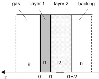
In Fig. 1 the geometry of a transmission detection configuration with two-layer sample, directly analyzed in this work, is given. Two-layer system consists of a layer (1) of thickness l1 (for example the thin modified layer or metal film) and layer (2) of thickness l2, where l = l1 + l2 is the thickness of the whole sample. This detected configuration implies the excitation of the sample on one side and detection of the acoustic response on the other side. This model was analyzed by several authors [6, 7] in accordance with the Rosencwaig-Gersho theory [8 ]. They have taken into account only the thermodiffusion mechanism of the generation of the PA signal. However, the thermoelastic mechanism can have an important influence on the PA signal, especially at higher frequencies [9].
The PA effect in a semiconductor is based on plasma, thermal and elastic waves generation in the material and the investigation of effects of their propagation. The most common mechanism of wave generation is the absorption of an intensity modulated light
beam by a material. The time periodic photoexcitation of electron-hole pairs, i.e. the plasma wave and generation of periodic heat and mechanical vibrations, i.e., thermal and elastic waves, can be manifested in various ways. One is a sound
generation (the PA effect), or an optical probe beam deflection (the PT deflection), or an infrared emission (the PT radiation), etc.
The PA and PT effects in semiconductors have been explained by many authors. Mikoshiba et al [ 10 ] and Vasil'ev and Sandomirskii [ 11 ] gave first model for the PA effect in semiconductors by taking into account the behavior of carriers under time-varying excitation, namely the diffusion, interband and surface recombination and intraband relaxation of carriers. The theory of the PA effect in a homogeneous semiconductor in the presence of an electric field was presented by Bandiera et al [12]. Sablikov and Sandomirskii [13 ] developed the theory of the PA effect for a homogeneous semiconductor taking into account the influence of
l1
g
l2
b
gas
layer 1
layer 2
backing
0
l1
l1+l2
z
l1
Fig. 1 Gas-sample (two-layer)-backing (gas) detection configuration with cylindrical cross-section.
2001 © The Japan Society for Analytical Chemistry
s137
ANALYTICAL SCIENCES APRIL 2001, VOL.17 Special Issue
energy band bending. The theory of Kino and Stearns [14] included the electronic deformation mechanism in photoacoustic effect. Gusev [15] has considered the role of free-carriers in the process of photogeneration of longitudinal acoustic waves in semiconductors. The linear theory of longitudinal acoustic wave generation in the case of interband absorption of optical radiation was given by Gusev and Petrosyan [16].
Many authors [17, 18] gave a general theoretical framework for the interpretation of the photothermal and photoacoustic signals produced in nonhomogeneous semiconductors, characterized by a p-n jup-nctiop-n. Fourp-nier et al [19] developed the optical beam deflectiop-n (OBD) technique to determine the electronic transport parameters (the carrier diffusivity, the carrier lifetime and the surface recombination velocity). For characterization of semiconductor materials, especially for general monitoring of semiconductor wafers quality, is important the modulated optical reflectance (MOR) technique developed by Rosencwaig et al [20].
Mechanisms of PA signal generation
There are three mechanisms of the PA signal generation in the semiconductor with a gas-sample-gas detection configuration (Fig.1). The propagation of thermal waves through the sample and through the surrounding gas, which is in contact with the sample, produces acoustic waves in gas. This is the so-called thermodiffusion (TD) mechanism of PA generation. On the other hand, the thermal waves in the sample cause the elastic vibrations, which propagate to the sample surface where then cause expansion and contraction of the surrounding gas, i.e. an acoustic wave [11]. This is the thermoelastic (TE) mechanism of PA generation. Also, semiconductor materials show a mechanical straining when electron-hole plasma is generated. The photoexcited free carriers produce directly a periodic elastic deformation in the sample - electronic deformation (ED), which in turn generates an acoustic wave [16].
In order to find the excess carrier density distributions, ∆n1 (z,ω), ∆n2 (z,ω), the periodic temperature distributions, φ1(z,ω),
φ2(z,ω) and elastic displacements (the thermoelastic and
electronic deformation bending), uTE(r,z,ω), uED(r,z,ω), the
plasma, heat and elastic diffusion equations needed to be solved in both layers. The energy gap is assumed to be the same for both layers and sg, si and sb are the recombination velocities of the
modified surface, interface and back surface, respectively. The appropriate boundary conditions, which result from the continuity of the carrier density and temperature distributions at various interfaces, are done. Four boundary conditions can be written for carrier density continuity and flux conservation at the interface z=l1, at surfaces z=0 and z=l2. Also, four additional boundary conditions from the continuity of the temperature distribution and heat fluxes at the interfaces enable to find the integration constants in relationships for carrier density and temperature distributions.
The general theoretical analysis consists of modeling a complex system of a gas-sample-gas detection configuration. Using the McDonald-Wetsel composite piston model [11], the PA signal S(ω), can be given as a sum of the thermodiffusion STD(
ω), thermoelastic, STE (
ω) and electronic deformation, SED(ω), components.
The TE and ED effect contributions to the PA signal were experimentally and theoretically analyzed in recently published papers by Todorovic et al. [ 21 , 22 ]. The TE and ED effect contributions to the PA signal in semiconductors were analyzed using the relation for quasistatic elastic bending derived by the theory of thin plate vibrations. A review of TE and ED mechanisms in semiconductors was done by Todorovic and Nikolic [23].
The elastic deformation in the sample can be analyzed using the stress-strain relation and appropriate equations of motion as functions of elastic displacements. The sample is illuminated on one side with an intensity-modulated non-focused laser beam with a circular spot. It is assumed that the spot-size a is on the order of the plate radius R. In accordance with the elastic theory of a thin plate with rotational symmetry, the quasistatic elastic displacements (the elastic bending), uTE(r,z,ω), uED(r,z,ω), were
obtained.
The quasistatic elastic displacements, in the case of simply supported circular plate boundary conditions, were obtained. The TE and ED generation mechanisms were analyzed in the case of a
101 102 103 104 105 10-10 10-9 10-8 10-7 10-6 10-5
m o d. f r e q u e n c y [ H z
]
]
P A
a
m
p l
i t
u d
e
[
a
.u
.
]
E D
T E
T D
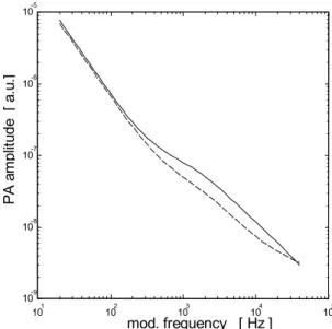
Fig. 2(a) Amplitude PA components of the two-layer sample: (- -) TD component; (...) TE; (-.-) ED component; ( - ) sum of the components.
101 102 103 104 105 -300 -200 -100 0 mod. frequency [ Hz ] PA phase [ de g ] ED TD TE
Fig. 2(b) Phase PA components of the two-layer sample: (- -) TD component; (..) TE; (-.-) ED component; (-) sum of the components.
one-layer sample. Taking into account that the wavelength of elastic waves is much longer than sample thickness; one can treat the sample as a monolayer if one layer is much thinner than the other layer (thin film-substrate). Then the elastic phenomenon is observed only in the thicker layer (substrate).
Analysis of PA signals
This theoretical model is suitable for analysis of various practical configuration as the epitaxial film-semiconductor substrate; metal-semiconductor junction (the Schottky barrier-depletion layer, i.e. the space charge region, and quasi-neutral region); ion-modified layer on semiconductor substrate, etc.
The calculation procedure is made using optical (the coefficient of optical absorption), the thermal (the thermal diffusivity, DT), elastic (the coefficient of thermoelastic expansion, αT, the coefficient of electronic deformation, d), the carrier transport parameters (the carrier diffusion coefficients, DE, the carrier lifetimes τ, the carrier surface recombination velocities, sj) and the geometrical parameters (the thicknesses l, l1, and l2 , the sample radius R and optical excitation beam spot, a.
Fig. 2 shows the typical calculated components of amplitude and phase PA signal for two-layer sample (the epitaxial film on Si substrate). Theoretically calculated curves were obtained for the following parameters:
(a) layer 2 (Si substrate): the thicknesses l2 = 290 µm, the optical absorption coefficient α2=5x103 cm-1; thermal diffusivity DT2=0.9
cm2/s; the coefficient of thermal expansion α
T2=2.3x10⁻⁶ 1/K; the
excitation energy E=1.96 eV; the coefficient of electronic deformation d2 = -9x10 - 25 cm3; the carrier diffusivity DE2 = 20
cm2/s; the excess carrier lifetime τ
2 =5x10 -5 s;
(b) layer 1 (epitaxial film): the thicknesses l1 = 10 µm, the optical absorption coefficient α1=1x104 cm-1 and it has the same values
for sound velocities v1=v2=5x105 cm/s; the energy gap EG=EG2 = 1.11 eV, d1 = d2 , while the excess carrier lifetime decreases τ1 =5x10 -6 s, DT1=0.75 cm2/s and carrier diffusivity DE1=5 cm2/s. The effective surface recombination velocities are: front surface
recombination velocitysg=1000,interface recombination velocity
is si=1000 and back surface recombination velocity sb=500 cm/s.
The validity of the two-layer model was verified by comparison with model for one-layer sample. For this purpose, in calculation with one-layer model the sample thickness is same as the total thickness of the two-layer sample (l=l1+l2), the surface
velocity recombination at the interface z=l1, was taken equal to
zero, and other physical parameters were same as for substrate (layer 2) in two-layer model. Fig.3 shows the comparison of the calculated PA amplitude for two-layer model with PA amplitude for one-layer model. Figure 3 shows that the PA amplitude for two-layer sample is significant different than the PA amplitude for one-layer sample at frequencies above ~100 Hz, where the thermal and electronic characteristics of thin layer become important.
Previously given analysis shows that the two-layer model has the significant application in many practical PA detection configurations. Examples of application of this model are in investigation of an implanted layer on crystalline silicon [24], and Schottky barrier-depletion region [25].
References
1. A.Rosencwaig, in Photoacoustic and Thermal Wave Phenomena in Semiconductors, ed. A.Mandelis, 1987, North Holland, New York, Chap.5.
2. J.Opsal, A.Rosencwaig, Appl.Phys.Lett., 1985, 47(5), 498-500. 3. J.Opsal, M.W.Taylor, W.L.Smith, and A.Rosencwaig,
J.Appl.Phys, 1987, 61, 240.
4. S.Wurm, P.Alpern, D.Savignac, and R. Kakoschke, Appl.Phys.A, 1988 , 47, 147.
5. C.Christofides, F.Diakonos, A.Seas, C.Christou, M.Estoros, and A.Mandelis, J.Appl.Phys.,1996, 80, 1713.
6. S.Vinokurov, J.Eng.Phys., 1983, 44, 50.
7. T.Tominaga and K.Ito, Jap.Appl.Phys., 1988, 27, 2392. 8. A. Rosencwaig, and A. Gersho, J. Appl. Phys., 1976, 47(1), 64. 9. F.McDonald, and G.Wetsel, J.Appl.Phys. 1978, 49(4), 2313. 10. N.Mikoshiba, H.Nakamura, K.Tsubouchi, IEEE 1981 Ultrasonics Symposium Proceedings, Dalas, 1981, (Cart. No.84 Ch 2112-1), vol.1, 443.
11. A.N.Vasil'ev, V.B.Sandomirskii, Sov. Phys. Semicond., 1984, 18, 1095.
12. J.Bandiera, H.Closs, C.Ghizoni, J. Photoacoustics, 11982, 1, 275.
13. V.A.Sablikov, and V.B.Sandomirskii, Phys.Stat.Sol(B), 1983, 120, 471.
14. G.S.Kino, and R.G.Stearns, Appl. Phys. Lett., 1985, 49, 926. 15. V.E.Gusev, Akust. Zhurn., (USSR), 1986, 32(6), 778. 16. V.E.Gusev, and E.G.Petrosyan, Akust. Zhurn., (USSR), 1987, 33(2), 223.
17. Yue-sheng Lu, Shu-yi Zhang, and Jian-chun Cheng, J.Appl.Phys., 1990, 68(3), 1088.
18. A.Mandelis, J.Appl.Phys., 1989, 66(11), 5572. 19. D.Fournier, A.C.Boccara, A.Skumanich and N.M.Amer, J.Appl.Phys., 1986, 59(3), 787 .
20. A.Rosencwaig, J.Opsal, W.L.Smith, D.L.Willenborg, Appl.Phys.Lett., 1985, 46(11), 1013.
21. D.M.Todorovic, P.M.Nikolic, A.I.Bojicic, K.T.Radulovic, Phys. Rev.B, 1997, 55(23), 15631.
22. D.M.Todorovic, P.M.Nikolic, A.I.Bojicic, J.Appl.Phys., 1999, 85(11), 7716. 101 102 103 104 105 10-9 10-8 10-7 10-6 10-5 mod. frequency [ Hz ] PA a m pl itude [ a. u. ]
Fig. 3 Comparison of two-layer model with one-layer model. PA amplitude of Si disk: (- -) one-layer sample (l=300 µm) and ( - ) two-layer sample (l1=290 µm, l2=10 µm).
s139
ANALYTICAL SCIENCES APRIL 2001, VOL.17 Special Issue
23. D.M.Todorovic, P.M.Nikolic, in Semiconductors and Electronic Materials, Progress in Photothermal and
Photoacoustic Science and Technology, eds A.Mandelis, P.Hess, Optical Engineering Press, 1999, Ch. 9.
24. D.M.Todorovic, P.M.Nikolic, A.I.Bojicic, J.Elazar,
M.Smiljanic, R.Petrovic, D.G.Vasiljevic-Radovic, K.T.Radulovic, 11 International Conference on Photoacoustic and Photothermal Phenomena, Kyoto, Japan, 2000, paper A-26-p6.
25. D.M.Todorovic, and M.Smiljanic, 11 International Conference on Photoacoustic and Photothermal Phenomena, Kyoto, Japan, 2000, paper P-06-05.