JAIST Repository: 電極材料の異なるC60電界効果トランジスタの作製と評価
6
0
0
全文
(2) Fabrication and device characteristics of C60 field-effect transistor with electrodes of different materials Nobuya Takahashi School of Material Science, Japan Advanced Institute of Science and Technology. Abstract Introduction Organic field-effect transistors (OFETs) have great potential for next-generation electronic devices because of their inexpensive price, light weight, mechanical flexibility. Performance of OFETs has been dramatically improved, and the mobility has become comparable to that of amorphous Si (a-Si) during recent years.1-3 From the systematic and detailed characterization of OFETs,4-8 it has been clarified that the device performance of OFETs strongly depends on parasitic resistance at the interface between the source/drain electrodes (an inorganic metal) and the channel (an organic semiconductor). Dominant origin of the parasitic resistance was thought to be the Schottky barrier at the interface between electrodes and the channel. Simply, the barrier height is estimated by Mott-Schottky relationship, namely, the energy difference between the Fermi energy (EF) of an electrode and the energy level of the lowest unoccupied molecular orbital (LUMO) ELUMO of an organic semiconductor for electrons, and that between EF of an electrode and the energy level of the highest occupied molecular orbital (HOMO) EHOMO of an organic semiconductor for holes. Actually, by reducing the energy difference between the EF and ELUMO (EHOMO), the device performance of n-type (p-type) FETs including field-effect mobility μFE was improved.6,7 Local electronic structure at the interface between an inorganic metal and an organic material has also been vigorously investigated. Experimental9 and theoretical10,11 studies showed that charge transfer between metals and molecules occurs, and the valence of molecules at the interface is not neutral. Appearance of dipole moment at interface induced by a charge transfer was also proposed. From these studies, it was clarified that the carrier injection barrier can be attributed not only to the Mott-Schottky relationship, but also to the effects of vacuum-level shift and local electric dipole due to the charge transfer and hybridization between an inorganic metal and an organic material. For the application of OFETs to electronic devices, such as complementary metal-oxide semiconductors (CMOS), detailed characterization of contact resistance and development of electrodes available to both p- and n-type OFETs are required. Indium tin oxide (ITO) is well known as a transparent anode for organic light emitting diodes (OLEDs). Furthermore, it is also expected to be used for source/drain electrodes of n-type OFETs, because work function φ of ITO is smaller than those of typical electrode materials of n-type OFETs such as Au.. I.
(3) In the present study, C60 FETs with source/drain electrodes of three different materials, ITO (In2O3 + SnO2 10 wt%), Au, and Pt have been fabricated, and devices characteristics were investigated.. Experiments C60 FETs were fabricated with a bottom contact configuration as shown in Fig. 1. A heavily doped n-type silicon wafer with 400 nm thickness of thermally oxidized SiO2 layer on the surface was used as substrate. The source and drain electrodes were patterned on insulating SiO2 layer, using a photolithography method: the channel length L and the channel width W were designed to be 5-25 and 500 μm, respectively. For the devices with electrodes of ITO, a film was deposited using RF magnetron sputtering (Tokuda CFS-4ES) at a nominal deposition rate of 0.4 nm/s under argon flow at the pressure of 0.50 Pa. For the devices with electrodes of Au or Pt, films of Au and Pt were deposited using DC sputtering (Elionix ECS101) at a deposition rate of about 0.06 and 0.08 nm/s, respectively. The thickness of source/drain electrodes was fixed to be 100 nm independent of the electrode materials. The doped silicon layer of the wafer was used as a gate electrode. Commercially available C60 (99.98 %) was used for the formation of the thin films channel layer. A C60 thin film of 150 nm thickness was formed using vacuum (< 10-5 Pa) vapor deposition at the deposition rate of 0.1 nm/s. FETs fabricated by this procedure were exposed to air during the transfer from the deposition chamber to a measurement chamber. Before measurements, therefore, the samples were annealed at 120 ºC under 10-3 Pa for 24 hours in order to remove adsorbed O2 and/or H2O molecules. Transport properties of C60 FETs were measured at room temperature under 10-3 Pa without exposure to air after annealing using prober system (Desert TT-prober, Keithley 4200-SCS). In this study, in order to reduce the influence of the small number of adsorbed O2 and/or H2O molecules, all fabrication and experimental processes of three types of devices except for the deposition of source/drain electrodes was performed under the same condition. In addition, more than three series of these experiments were repeated, and data were compared within the same series. For the estimation of φ of ITO, Au, and Pt, the films of these materials fabricated by the same procedure were investigated by photoemission (PE) spectroscopy (Riken Keiki AC-2).. Source C60 Drain SiO2 n+-Sii (Gate). Fig.1. Device structure of C60 FET in this work.. II.
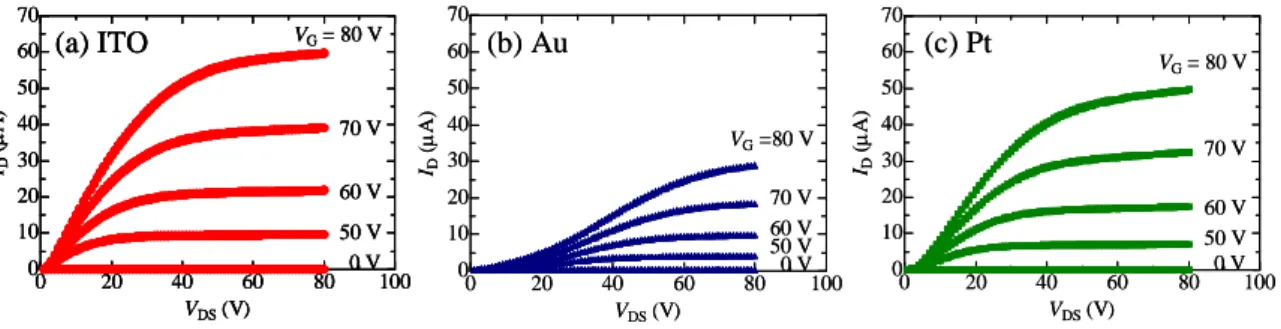
(4) Results and Discussions Figure 2 (a)-(c) shows the output characteristics, namely the drain current ID versus the drain-source voltage VDS plots, for C60 FET with source/drain electrodes of ITO, Au, and Pt. ID increases almost linearly with increasing VDS, followed by saturation due to the pinch-off of the accumulation layer; all FETs in this work show typical n-type normally-off characteristics. Hysteresis of ID’s with VDS sweep was very small.. 70. 70 VG = 80 V. (a) ITO. 60. 40. 70 V. 30. ID (μA). ID (μA). 60. 50. 50. 60 V. 20. 50 V 0V 80 100. 10. 20. 40 60 VDS (V). VG =80 V. 30. 10. 0 0. (c) Pt. VG = 80 V. 50. 40. 20 0 0. 70. (b) Au ID (μA). 60. 20. 40 60 VDS (V). 70 V 60 V 50 V 0V 80 100. 40 70 V. 30 20. 60 V 50 V 0V 80 100. 10 0 0. 20. 40 60 VDS (V). Fig.2. ID vs VDS plots for C60 FET with source/drain electrodes of (a) ITO, (b) Au, (c) Pt. Gate voltage were applied from 0 to 80 V with 10 V step. The plots of ID1/2 versus the gate voltage VG for all 10. threshold voltage VT were determined from the relation,. 8. ID = (μFEWC0/2L)(VG-VT)2, at saturation regime. μFE and VT were 1.6 x 10⁻¹ cm2/Vs and 36 V for the device with. ID1/2 (μA1/2). devices at VDS = 80 V are shown in Fig. 3. The μFE and. ITO. VDS = 80 V. Pt Au. 6 4. ITO source/drain electrodes, 9.6 x 10⁻² cm2/Vs and 42 V. 2. for that with Au electrodes, and 1.4 x 10⁻¹ cm2/Vs and 41. 0 0. 20. 40 60 VG (V). 80. 100. V for that with Pt electrodes, respectively. Here, we use 1.0 x 10⁻⁸ F/cm2 as the capacitance per area of gate insulator SiO2 (C0) estimated from dielectric constant and. Fig.3. ID1/2 vs VG plots at VDS = 80 V for all C60 FET.. thickness of SiO2. PE spectra of the films of ITO, Au, and Pt are shown in Fig. 4(a). The square root of intensity IPE1/2 was proportional to energy of incident light E for all samples. φ was determined as threshold energy ET from the relation, IPE1/2 = a(E-ET) + b, where a is just a fitting parameter, and b is background. Values of estimated φ are summarized in Fig. 4(b) with energy diagram. They are consistent with those in the literature.12,13 ELUMO and EHOMO of C60 are taken from Refs. 14 and 15 as 3.57 eV, and 6.17 eV, respectively.. III.
(5) 100. 2. (a). Au (x 2) Pt. 60 40 20. 0 4. Vacuum level. 0 E (eV). 1/2. 1/2. (cps ). 80. IPE. (b). ITO (x 4). -2 -4 -4.7 eV. -4.9 eV. -5.0 eV. -6.17 eV EHOMO. -6 4.5. 5. 5.5 E (eV). 6. 6.5. 7. -3.57 eV ELUMO. -8. ITO. Au. Pt. C60. Fig.4. (a) PE spectra of the firm of ITO, Au, and Pt. (b) Energy diagram of ITO, Au, Pt, and C60. From these values, the expected Schottky barrier heights at the interface between electrodes of ITO, Au, Pt and C60 are 1.13, 1.33, 1.43 eV, respectively. It was reported that the device performance of C60 FETs is affected by large contact resistance between electrodes and the channel of C60,8 which results in lower values of μFE.7: FETs with lower carrier injection barriers show higher values of μFE. Consistent with this analogy, μFE of an FET with ITO electrodes is the highest among the three types of FETs in this study. The result shows that ITO, which is one of the typical hole-injection electrodes for p-type organic semiconductors, can also be a good electron-injection electrode for n-type organic semiconductors such as C60. In addition, ITO provides very stable electrodes with small φ, whereas metal electrodes with small φ are very sensitive to air and should be used in vacuum.6,7 This implies that the use of ITO as an electrode is very effective for transparent organic electronic devices containing both p- and n-type FETs, such as CMOS. μFE of the FET with Pt electrodes, which was expected to be the lowest among FETs in this work, is higher than that of FET with Au electrodes, and is very close to that of FET with ITO electrodes. We repeated the same series of experiments more than three times. In these experiments, the trend was invariant, although absolute values of device parameters varied slightly in each series. The origin of this discrepancy from Mott-Schottky limit may be attributed to modification of local electronic structure at the interface between electrodes and C60 due to charge transfer and/or hybridization of orbitals such as π-d interaction.9-11. Conclusion In conclusion, C60 FETs with source/drain electrodes of three different materials, ITO, Au, and Pt have been fabricated and investigated. The highest μFE value of 1.6 x 10⁻¹ cm2/Vs in this work has been obtained in the C60 FETs with ITO electrodes, showing that ITO can be used not only for the hole-injection electrodes for p-type organic semiconductors, but also for the electron-injection electrodes for n-type organic semiconductors such as C60. This implies that the use of ITO as an. IV.
(6) electrode will contribute to development of transparent organic electronics. μFE of the FET with Pt electrodes, which was expected to be the lowest among FETs in this work, is higher than that of FET with Au electrodes. The result suggests the modification of local electronic structure at the interface between electrodes and a channel of C60 due to charge transfer and/or hybridization of orbitals.. References [1] S. Kobayashi, T. Takenobu, S. Mori, A. Fujiwara, and Y. Iwasa, Appl. Phys.Lett. 82, 4581 (2003). [2] V. Podzorov, E. Menard, A. Borissov, V. Kiryukhin, J. A. Rogers, and M. E. Gershenson, Phys Rev. Lett. 93, 086602 (2004). [3] K. Itaka, M. Yamashiro, J. Yamaguchi, M. Haemori, S. Yaginuma, Y. Matsumoto, M.. Kondo, and H. Koinuma, Adv. Mater. 18, 1713 (2006). [4] I. Yagi, K. Tsukagoshi, and, Y. Aoyagi, Appl. Phys. Lett. 84, 813 (2004). [5] B. H. Hamadai and D. Natelson, J. Appl. Phy. Lett. 95, 1227 (2004). [6] T. Ohta, T. Nagano, K. Occhi, Y. Kubozono, E. Shikoh, and A. Fujiwara, Appl. Phys. Lett. 89, 053508 (2006). [7] K. Ochi, T. Nagano, T. Ohta, R. Nouchi, Y. Kubozono, Y. Matsuoka, E. Shikoh, and A. Fujiwara, Appl. Phys. Lett. 89, 083511 (2006). [8] Y. Matsuoka, K. Uno, N. Takahashi, A. Maeda, N. Inami, E. Shikoh, Y. Yamamoto, H. Hori and A. Fujiwara, Appl. Phys. Lett. 89, 173510 (2006). [9] B. W. Hoogenboom, R. Hesper, L. H. Tjeng, and G. A. Sawatzky, Phys. Rev. B57, 11939 (1998). [10] L. –L. Wang, and H. –P. Cheng, Phys Rev. B69, 045404 (2004). [11] L. –L. Wang, and H. –P. Cheng, Phys Rev. B69, 165417 (2004). [12] H. B. Michaelson, J. Appl. Phys. 48, 4729 (1977). [13] I. D. Parker, J. Appl. Phys. 75, 1656 (1994). [14] N. Sato, Y. Saito, and H. Shinohara, Chem. Phys.162, 433 (1992). [15] N. Hayashi, H. Ishii, Y. Ouchi, K. Seki, J. Appl. Phys. 92, 3784 (2002).. V.
(7)
図
関連したドキュメント
The necessity of the Wiener condition for equations of the monotone type was shown by Lindqvist and Martio [18] and Heinonen and Kilpel¨ ainen [11] with the restriction p > n −
In the first section we introduce the main notations and notions, set up the problem of weak solutions of the initial-boundary value problem for gen- eralized Navier-Stokes
Furthermore, the upper semicontinuity of the global attractor for a singularly perturbed phase-field model is proved in [12] (see also [11] for a logarithmic nonlinearity) for two
On figures 2 and 6, the minimum, maximum and two of the intermediate free energies discussed in subsections 3.5 and 6.5 are shown for sinusoidal and exponential histories with n =
Related to this, we examine the modular theory for positive projections from a von Neumann algebra onto a Jordan image of another von Neumann alge- bra, and use such projections
Next, we prove bounds for the dimensions of p-adic MLV-spaces in Section 3, assuming results in Section 4, and make a conjecture about a special element in the motivic Galois group
Maria Cecilia Zanardi, São Paulo State University (UNESP), Guaratinguetá, 12516-410 São Paulo,
In this paper we focus on the relation existing between a (singular) projective hypersurface and the 0-th local cohomology of its jacobian ring.. Most of the results we will present
