JAIST Repository
https://dspace.jaist.ac.jp/Title Photoconductivity of Single-Wall Carbon Nanotube Films
Author(s)
Fujiwara, A; Matsuoka, Y; Matsuoka, Y; Suematsu, H; Ogawa, N; Miyano, K; Kataura, H; Maniwa, Y; Suzuki, S; Achiba, Y
Citation Carbon, 42(5-6): 919-922 Issue Date 2004
Type Journal Article
Text version author
URL http://hdl.handle.net/10119/3358
Rights
Elsevier Ltd., A. Fujiwara, Y. Matsuoka, Y. Matsuoka, H. Suematsu, N. Ogawa, K. Miyano, H. Kataura, Y. Maniwa, S. Suzuki and Y. Achiba, Carbon, 42(5-6), 2004, 919-922.
http://www.sciencedirect.com/science/journal/0008 6223
PHOTOCONDUCTIVITY OF SINGLE-WALL CARBON
NANOTUBE FILMS
A. Fujiwara,*1,2 Y. Matsuoka,1,2 Y. Matsuoka,†3 H. Suematsu,‡3 N. Ogawa,4 K. Miyano,5 H. Kataura,6 Y. Maniwa,6 S. Suzuki,7 Y. Achiba7
1School of Materials Science, Japan Advanced Institute of Science and Technology,
1-1 Asahidai, Tatsunokuchi, Ishikawa 923-1292, Japan
2CREST, Japan Science and Technology Corporation,
4-1-8 Honchou, Kawaguchi, Saitama 332-0012, Japan
3Department of Physics, School of Science, The University of Tokyo,
7-3-1 Hongo, Bunkyo-ku, Tokyo 113-0033, Japan
4Department of Applied Physics, School of Engineering, The University of Tokyo,
7-3-1 Hongo, Bunkyo-ku, Tokyo 113-8656, Japan
5Research Center for Advanced Science and Technology, The University of Tokyo,
4-6-1 Komaba, Meguro-ku, Tokyo 153-8904, Japan
6Department of Physics, School of Science, Tokyo Metropolitan University,
1-1 Minami-osawa, Hachi-oji, Tokyo 192-0397, Japan
7Department of Chemistry, School of Science, Tokyo Metropolitan University,
1-1 Minami-osawa, Hachi-oji, Tokyo 192-0397, Japan
Abstract
Time-resolvedphotoconductivity measurements were carried out on single-wall carbon nanotube (SWNT) films at various temperatures. Photoconductivity excitation spectra show two clear peaks around 0.7 and 1.2 eV. Observed peaks in the spectra correspond to the optical absorption between symmetrical bands of semiconducting SWNTs. The analysis of this feature allows insight into the transport properties of semiconducting SWNTs. Signal profiles in the photoresponse at low temperatures depend strongly on the sample, while intensity of the photoresponse monotonously increases with a decrease in temperature for all samples. Photo-induced current for a sample decays rapidly after the laser pulse irradiation. For another sample, on the other hand, it decreases gradually and remains up to a few hundred nano seconds, showing the existence of trapping sites in the nanotubes.
* Corresponding Author: Tel. +81-761-51-1551; Fax +81-761-51-1535; E-mail:
† Present address: Network Service Systems Laboratories, NTT Corporation, 3-9-1 Midori-cho,
Musasino-shi, Tokyo 180-8585, Japan.
‡ Present address: Materials Science Division, SR Research Laboratory, Japan Synchrotron
Key words: Carbon nanotubes, Photoconductivity, Semiconductor, Transport properties PACS: 72.80R, 73.50.P, 72.20, 78.20
1. Introduction
Carbon nanotubes (NTs) [1] have attracted great attention as potential electronic materials because of the one-dimensional tubular network structure on a nanometer scale. The variety of band structures of the NTs, being either semiconducting or metallic depending on the chirality and the diameter of the tube [2,3], is also a novel feature. For applying NTs to electronic devices, more detailed transport properties of semiconducting single-wall carbon nanotubes (SWNTs) have to be individually clarified. To date, however, selective growth of NTs has not been achieved: both the semiconducting and metallic SWNTs can coexist even in a single bundle [4]. Although Collins et al. [5] demonstrated a method for leaving only the semiconducting SWNTs from the mixture of semiconducting and metallic ones by burning only the metallic ones, this technique is quite difficult. To overcome this difficulty, we proposed photoconductivity measurements [6-10]. The photoconductivity excitation spectra show two peaks around 0.7 and 1.2 eV, which correspond to the first and second peaks of the optical absorption spectrum in semiconducting NTs, E11s and E22s [11,12]. By evaluating the properties of photoconductivity,
their own character of semiconducting SWNTs can be extracted from the mixture sample of semiconducting and metallic SWNTs. The photoconductivity of NTs has high potential not only to the practical application to the optical devices, such as high spatial resolution detector, nano-sized optical switch etc., but also to the fundamental characterization of the semiconducting NTs.
In this paper, we report on properties of photoconductivity originating from semiconducting SWNTs. We discuss variation of the temperature dependence of photoconductivity in terms of transport properties of semiconducting-SWNT circuits.
2. Experimental
The samples of SWNT bundles were synthesized by evaporation of composite rods of nickel (Ni), yttrium (Y) and graphite in helium atmosphere by arc discharge [12,13]. The diameter of the SWNTs used here is determined to be about 1.4 ± 0.2 nm by the Raman frequency of a breathing mode and TEM observation. The typical length of SWNT bundles estimated by scanning electron microscopy (SEM) is a few micrometers. To prepare film samples, soot-containing SWNTs was dispersed in methyl alcohol by ultrasonic vibrator, and suspension of SWNTs was dropped on glass substrate. The typical film sample size is about 100 × 100 µm2 and the thickness of the film is between 300 and 500 nm. The samples were annealed in vacuum at 10-6 Torr and 673 K for 2 hours to remove the absorbed gasses and methyl alcohol from samples. A pair of gold electrodes separated by a 10 µm gap was evaporated in vacuum on to the surface of the film samples and connected to a dc regulated power supply (100 mV). The samples were mounted in a continuous-flow cryostat. For measurements on the temperature dependence, samples were cooled by flowing the vapor of liquid He in the temperature range from 10 K to room temperature (R.T.). As a light source, an optical parametric oscillator (OPO) excited by a pulsed Nd:YAG laser with the duration time of 5 ns was used. The photon energy was set to in the range of 0.5 to 2.8 eV. The temporal profiles of the laser pulse and the current were monitored with a digitizing oscilloscope. In order to reduce spurious ringing in the fast
3
pulse detection, we were obliged to use the input impedance of the oscilloscope (50 Ω) as the reference resistor despite the obvious disadvantage of lower sensitivity. The resistance of samples in the dark is ca. 100 Ω at R.T. and order of 1kΩ at around 10 K.
3. Results and Discussion
Fig. 1 shows temporal evolution of photo-induced current for various incident light intensities for sample #1 at 13.2 K. The current properly follow the laser pulse shape: signal profile with a 5 ns width can be observed and increases with an increase in incident light intensity. The oscillatory structure for time t > 10 ns is considered to be due to ringing in the circuitry. Here, we derived the signal intensity by fitting the first peak in the signal profile with a Gauss function. The relationship between the signal intensity and the incident light intensity for various photon energies is shown in Fig. 1(b). Below 10 µA, the signal intensity responds linearly to incident light intensity. On the other hand, it shows saturation behavior above 10 µA; this saturation is often observed under intense light intensity and might be due to lack of replenishment of carriers [14]. Therefore, we estimate the photoresponse from the deepest slope of the signal intensity vs. incident light intensity curves in Fig. 1(b).
Photon energy dependence of photoresponse, i.e., photoconductivity excitation spectra for two film samples of SWNTs #1 and #2 at room temperature are shown in Fig. 2. Optical absorption spectrum for the sample made by the same method is also presented as a reference. Two clear peaks in photoconductivity excitation spectra at R.T. are observed around 0.7 and 1.2 eV. These energies are very close to the first and second peaks of the optical absorption spectrum in semiconducting NTs with a diameter of 1.4 nm, E11s and E22s. Therefore they correspond to the
electron excitation between symmetrical bands of semiconducting NTs. From this result, we can conclude that the photoconductivity originating from the semiconducting SWNTs occurs, and that this technique can be used for studying the electronic transport properties of semiconducting NTs.
As a first step of extraction and study on transport properties of the semiconducting SWNTs, we focus on the most simple process: photocarrier produced by the laser pulse with the energy of
E11s ≈ 0.7 eV. Figs. 3(a) and (b) show the temporal evolution of photo-induced current for
various incident light intensities for samples #1 and #3 at R.T., respectively. Data at 13.2 K for the sample #1 in Fig. 3(c) show almost the same behavior to those at R.T., except for the enhancement in the intensity. On the other hand, they change drastically for the sample #3 at 10.2 K, as shown in Fig. 3(d). The current shows a pronounced tail superposing on the oscillatory structure after the first peak observed in Figs. 3(a)-(c). This tendency becomes remarkable at low temperatures.
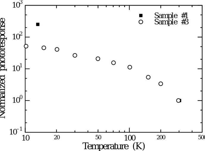
Temperature dependence of photoresponse normalized by the data at R.T. for samples #1 and #3 are shown in Fig. 4. Although photoresponse increases monotonously with a decrease in temperature in both samples, the degree of enhancement at low temperatures are different between these two samples. This difference is attributed to three reasons. One of them is an intrinsic behavior of semiconducting SWNTs. As shown in Fig. 3(d), the current is distributed to wide time scale, which cannot contribute to the photoresponse in Fig. 4, because we derived the photoresponse by fitting the first peak in the signal profile in the present definition. This behavior will be discussed later. Next one is the underestimation of photoconductive response at low temperatures in the sample #3. As discussed above the photocurrent does not respond linearly to incident light intensity but tend to saturate at high light intensity region. This effect is much larger in sample #3, because experiments were performed under rather high incident light intensity as shown in Figs. 3(b) and (c). Therefore, the effect of saturation on them becomes larger at higher intensity, namely, at lower temperature. This difference might be due also to differences in conditions of contact between SWNTs and/or SWNTs and electrode; loose
contacts can causes the reduction of photoconductive response at low temperatures where carrier must hop by thermal activation for conductance.
Considering rather small enhancement of the first-peak intensity and the tail in the signal profile of the current, it is plausible that trapping of photocarrier affect the photoconductive properties of the sample #3 at low temperatures. This result suggests that quality of semiconducting SWNTs is various even in the sample produced by the same method. Although this fact has not been pointed out clearly so far, it is very important information from the viewpoint of application of semiconducting SWNTs to electronic devices. In addition, our results show photoconductivity is very sensitive to the quality of semiconducting-SWNT circuits. Further experiments will clarify the mechanism of electron trapping in the semiconducting SWNTs.
4. Conclusions
We have investigated properties of photoconductivity in SWNT bundles. Photoconductivity excitation spectra show good correspondence to the optical absorption spectrum of the semiconducting SWNTs, showing that we can extract the transport properties of semiconducting SWNTs from the mixture sample of the semiconducting and the metallic SWNTs. Temporal evolution of profile and its intensity strongly depend on the sample and temperature. The origin of this variation is considered to be due to the difference in trapping effect of the circuits consisting of semiconducting SWNTs. This result suggests that quality of semiconducting SWNTs is various even in the sample produced by the same method, and that photoconductive properties are very sensitive to it. We can propose that photoconductivity measurements are very effective and powerful technique for evaluating electronic circuit and devices consisting of semiconducting SWNTs.
Acknowledgements
This work was supported in part by the JSPS "Future Program" (RFTF96P00104), the Grant-in-Aid for Scientific Research (A) (13304026) from the Ministry of Education, Culture, Sports, Science and Technology (MEXT) of Japan, and CREST of Japan Science and Technology Corporation. One of authors (A.F.) was supported by a Grant-in-Aid for Encouragement of Young Scientists (12740202) from the MEXT of Japan.
References
[1] Iijima S. Helical microtubules of graphitic carbon. Nature 1991;354:56-58.
[2] Saito R, Fujita M, Dresselhaus G, Dresselhaus MS. Electronic structure of chiral graphene tubules. Appl Phys Lett 1992;60(18):2204-2206.
[3] Hamada N, Sawada S, Oshiyama A. New one-dimensional conductors: graphite microtubules. A. Phys Rev Lett 1992;68(10):1579-1581.
[4] Fujiwara A, Iijima R, Ishii K, Suematsu H, Kataura H, Maniwa Y, Suzuki S, Achiba Y. Local current density detection of individual single-wall carbon nanotubes in a bundle. Appl Phys Lett 80(11);2001:1993-1995.
[5] Collins PG, Arnold MS, Avouris P. Engineering carbon nanotubes and nanotube circuits using electrical breakdown. Science 2001;292:706-709.
[6] Fujiwara A, Matsuoka Y, Suematsu H, Ogawa N, Miyano K, Kataura H, Maniwa Y, Suzuki S, Achiba Y. Photoconductivity in semiconducting single-walled carbon nanotubes. Jpn J Appl Phys 2001;40(11B):L1229-L1231.
5
[7] Fujiwara A, Matsuoka Y, Suematsu H, Ogawa N, Miyano K, Kataura H, Maniwa Y, Suzuki S, Achiba Y. Photoconductivity of single-walled carbon nanotubes. AIP Conference Proceedings 2001;590:189-192.
[8] Fujiwara A, Matsuoka Y, Iijima R, Suematsu H, Ogawa N, Miyano K, Kataura H, Maniwa Y, Suzuki S, Achiba Y. Photoconductivity and local transport properties of single-wall carbon nanotubes. AIP Conference Proceedings 2002;633:247-250.
[9] Matsuoka Y, Fujiwara A, Ogawa N, Miyano K, Kataura H, Maniwa Y, Suzuki S, Achiba Y. Temperature dependence of photoconductivity at 0.7eV in single-wall carbon nanotube films. Sci Technol Adv Mater 2003;4(1):47-50.
[10] Fujiwara A, Matsuoka Y, Ogawa N, Miyano K, Kataura H, Maniwa Y, Suzuki S, Achiba Y. Temperature dependence of photoconductivity of single-wall carbon nanotubes. Submitted to AIP Conference Proceedings.
[11] Ichida M, Mizuno S, Tani Y, Saito Y, Nakamura A. Exciton effects of optical transitions in single-wall carbon nanotubes. J Phys Soc Jpn 1999;68(10):3131-3133.
[12] Kataura H, Kumazawa Y, Maniwa Y, Umezu I, Suzuki S, Ohtsuka Y, Achiba Y.
Optical properties of single-wall carbon nanotubes. Synth Met 1999;103:2555-2558.
[13] Journet C, Maser WK, Bernier P, Loiseau A, Lamy de la Chapelle M, Lefrant S, Deniard P, Lee R, Fischer JE. Large-scale production of single-walled carbon nanotubes by electric-arc technique. Nature 1997;388:756-758.
List of Graphics Captions
Fig. 1. (a) Temporal evolution of photo-induced current for various incident light intensities for sample #1 at 13.2 K. (b) Incident light intensity dependence of photoresponse.
Fig. 2. Photoconductivity excitation spectra for two film samples of SWNTs (#1, #2) at room temperature. Optical absorption spectrum for the sample made by the same method is also presented with a dotted line as a reference. Background of optical absorption which is almost linearly increases with photon energy in this region was subtracted.
Fig. 3. Temporal evolution of photo-induced current for various incident light intensities for (a) sample #1 at R.T., (b) sample #3 at R.T., (c) sample #1 at 13.2 K, (d) sample #3 at 10.2 K.
Fig. 4. Temperature dependence of the photoresponse at 0.7 eV for the samples #1 and #3 normalized by the data at R.T.
7 Fig. 1.
0
20
40
60
80
100
Photon power (nJ/pulse)
0
20
40
60
80
100
Si
gnal
i
n
te
ns
it
y (
µ
A)
(b)
0.554 eV
0.581 eV
0.658 eV
0.740 eV
0.831 eV
0.932 eV
1.049 eV
1.193 eV
1.500 eV
0
5
10
15
20
Time (ns)
0
20
40
60
80
100
C
u
rren
t (
µ
A)
Sample#1 13.2 K
(a)
nJ/pulse
0.57
2.85
8.18
24.16
Fig. 2.
0.0
0.5
1.0
1.5
2.0
2.5
3.0
Photon energy (eV)
0.0
0.5
1.0
Phot
or
es
ponse
(
1
0
3A
/J
V
)
0.0
0.5
1.0
Opt
ical
dens
it
y
(
arb. uni
ts
)
R.T.
(
×
0.25)
Sample #1
Sample #2
9 Fig. 3. 0 5 10 15 20
Time (ns)
0 50 100Curr
ent (
µ
A)
(c) #1 13.2 K nJ/pulse 0.57 2.85 8.18 24.16 0 20 40 (a) #1 R.T. nJ/pulse 130 240 500 910 0 20 40 (b) #3 R.T. nJ/pulse 1470 826 202 145 0 5 10 15 20 25 30 35 40 0 200 400 (d) #3 10.2 K nJ/pulse 1420 804 174 114Fig. 4.