SUMMARY This paper introduces a formation method for 3- dimensional 6 ch.×6 ch. shuffling structures withgraded-index (GI)cir- cular core in a multimode polymer optical waveguide for optical printed circuit boards (OPCBs) using a unique photomask-free fabrication tech- nique named the Mosquito method. The interchannel pitch of the fabri- cated waveguides is 250µm, where all the channels consist of both hor- izontal and vertical bending structures and the last 6 channels in parallel cross over the first 6 channels. We also report 3-dimensional S-shaped polymer waveguides. In the S-shaped waveguides, the first and last 6 chan- nels with both horizontal and vertical core bending composing the above 3-dimensional shuffling waveguide are separated, in order to evaluate the effect of over-crossing on the loss. It is experimentally confirmed that there is no excess insertion loss due to the shuffling structure in the 3-D shuf- fling waveguide. The evaluated crosstalk of the 3-D shuffling waveguide is lower than−30 dB. The 3-D shuffling waveguide proposed in this paper will be a promising component to achieve high bandwidth density wiring for on-board optical interconnects.
key words: polymer waveguides, 3-dimensional channel-shuffling struc- ture, multimode GI circular core, optical printed circuit boards (OPCBs)
1. Introduction
Over the last three decades, the rapid advances of opti- cal communication devices have improved telecommunica- tion and data communication network architectures tremen- dously. Recently, the wide deployment of cloud computing services has accelerated the ever-increasing demands to em- ploy optical data links even into computing systems. In ad- dition, the rapid development of microelectronic chips has raised the demand for optical interconnect which realizes extremely high data transfer rates[1]–[3]. Optical intercon- nects have been gradually replacing conventional copper- based electrical wiring because of their higher bandwidth density links with lower crosstalk. Consequently, optical in- terconnects are undisputedly anticipated to sustain the fur- ther growth of high-performance computers (HPCs)[4],[5].
In fact,multimode fiber (MMF)based optical links have al- ready been deployed in the rack-to-rack and board-to-board networks in some HPCs[6]. Although the optical/electrical (O/E) signal conversions take place at the edge of the board in current MMF links, it is highly desirable to place the O/E and E/O conversions as close to the LSI chips as possi- ble[7]. So, optics for on-board and intrachip is the next key
Manuscript received October 30, 2017.
Manuscript revised January 24, 2018.
∗This is an original article.
†The authors are with Faculty of Science and Technology, Keio University, Yokohama-shi, 223–8522 Japan.
a) E-mail: ofr [email protected]
DOI: 10.1587/transele.E101.C.509
issue towards the further evolution of HPC systems.
Polymer optical waveguides are one of the promis- ing technologies[8]–[10]for realizing such short-reach high bandwidth density on-board optical interconnects. Opti- cal printed circuit boards (OPCBs) embedded with multi- mode polymer waveguides have been drawing much atten- tion[11], because of their easy integration with PCB, low material and processing costs. In particular, over the last couple of years, the feasibility of OPCBs with step-index (SI)core multimode waveguides have been investigated ex- tensively. However, in SI core polymer waveguides, the sur- face roughness on the core-cladding boundary causes ex- cess scattering loss and large crosstalk if multiple cores are aligned with a narrow interchannel pitch. Hence, we have reported a great advantage ingraded-index (GI)core poly- mer waveguides: low scattering loss at the core-cladding boundary, high speed data transmission capability, and high coupling efficiency with GI core MMFs: these advantages are mainly attributed to the strong optical confinement ef- fect of GI cores[12]–[14].
Over the last couple of years, several reports of GI core polymer waveguides fabricated applying conventional photo-lithography methods have been published[15], but the refractive index profiles in those fabricated waveguides are not necessarily symmetric. In contrast, the photo- addressing method[16] reported from Sumitomo Bakelite is a promising technique to form a square shaped core with ideally symmetric GI profiles. However, for the photo- addressing method, the applicable materials have been lim- ited only to polynorbornene resins. In addition, as the pho- tomasks are needed for the photo-addressing method, the core-cladding structure needs to be formed layer by layer in order to fabricate multiple layered waveguide structures.
On the contrary, we have developed a unique photomask- free fabrication method named the Mosquito method for fabricating GI circular core waveguides[17]. A commer- cially available microdispenser system with a desktop robot is utilized in the Mosquito method. One of the advantages of the Mosquito method is in its ability to easily form 3- dimensional wiring patterns.
The structures of channel shuffling in polymer waveg- uides have received much attention over the last couple of years. Most of the channel shuffling waveguides developed by the other research groups are fabricated applying pho- tolithography. Hence,step-index (SI)square cores are gen- erally formed, and the shuffling structures are involved in one plane, in which core crossings on one plane are re- Copyright c2018 The Institute of Electronics, Information and Communication Engineers
Fig. 1 The procedure of the Mosquito method
quired as well as curved structures. So, the crossing and bending losses are concerned. In addition, high coupling loss is another concern when the waveguides are connected with GI MMF, due to the core shape mismatch. Therefore, in this paper, a 3-dimensional shuffling structure is realized with horizontal and vertical core bending as well as multi- layer crossover structures of GI circular cores. This struc- ture would be very difficult to form using the conventional photolithography process.
2. The Mosquito Method
2.1 Fabrication Procedure
The detailed steps of the fabrication procedure are shown in Fig. 1.
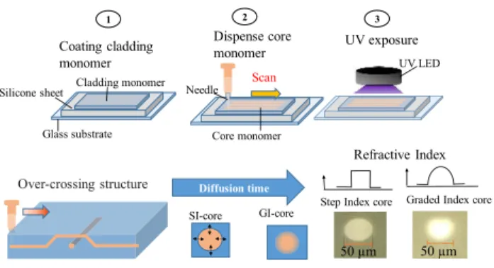
First, a liquid-state cladding monomer is coated on a glass substrate within a rectangular-shaped frame made of a silicone rubber sheet placed on the substrate, while an- other liquid-state core monomer is put into a syringe that is connected to a microdispenser. Next, the core monomer in the syringe is dispensed directly into the cladding monomer from the tip of the needle of the syringe. The syringe is set to a desktop robot to scan horizontally and vertically while maintaining its needle tip inserted into the cladding monomer. Since both the core and cladding monomers are in the liquid state, if an appropriate interim time is taken af- ter dispensing the core monomer until UV curing starts, con- centration distributions of the monomers are formed. Af- ter curing the monomers, the concentration distributions are fixed, resulting in a gradual variation in the refractive index around the core-cladding boundary. By optimizing the in- terim time, waveguides with ideally parabolic GI profiles are formed in the circular cores. After the UV curing step, post- baking at 150◦C is carried out for approximately 20 min- utes[18]. The core diameter is controlled to a desired value by adjusting the dispensing pressure and needle-scan veloc- ity, and actually the waveguides with almost 50-µm core diameter are obtained, while even single-mode waveguides with less than 10-µm cores are also fabricated[19],[20].
Fig. 2 Design of the needle tip path for the 3-dimensional 6 ch. x 6 ch.
shuffling polymer waveguide: (i) side and (ii) top view
2.2 3-Dimensional Graded-Index Shuffling Polymer Waveguide
The design for the 3-dimensional shuffling polymer wave- guide to be fabricated is shown in Fig. 2. This wiring pat- tern is realized by modifying the needle-scan program of the desktop robot. Figure 2 shows the needle-tip paths: Fig. 2 (i) is the side view from which how the cores are over-crossing is visualized in the depth direction. Meanwhile, the top view in Fig. 2 (ii) shows the shuffling structure in more detail.
From Fig. 2 (i), it is found that the needle tip scans for all the cores start from a height of 0.620 mm from the bottom of the cladding, which is defined as thereference position.
Then, for the first 6 channels (Ch. 1 to Ch. 6 in blue color), the needle tip path is gradually bent downward linearly to a height of 0.380 mm lower than thereference positionover a lateral distance of 30 mm: these are also horizontal bending to shuffle the channels. After reaching the lowest height, the needle tip is vertically bent upward to a height of 0.240 mm lower than the reference positionover a lateral distance of 17 mm, and then gradually raised to the reference position over a 30 mm lateral distance. Simultaneously, the needle tip path is also bent horizontally.
Similarly, for the last 6 channels (Ch.7 to Ch. 12 in orange color), the needle tip path is gradually bent upward to a height of 0.380 mm from thereference positionto the crossing section over a lateral distance of 30 mm, with hori- zontal bending. Then, the needle tip descends to a height of 0.135 mm from the top height (0.380 mm) over a 17-mm lat- eral distance at the crossing section, followed by a shallow slope to thereference positionover a 30-mm lateral distance.
Thus, the last 6 channels are placed above the first 6 chan- nels with height differences of 0.760 mm and 0.485 mm at the starting and ending sides of the crossing section, respec- tively. According to our investigation, for the core/cladding material pair employed in this paper, the bending radius should be larger than 2 mm so as not to cause extra bending loss: shallower crossing angles should be selected to allow forming over crossing structure inside the thinner cladding layer without disarray of the core. The interchannel pitch of this shuffling waveguide is set to 250µm, while the crossing angle and bending radius are 10◦ and 3 mm, respectively.
The needle tip path is bent up and down for the channels on both levels (orange and blue colors) to add a height differ- ence at the crossing section with a gentle bending of cores.
In order to make a uniform interchannel pitch, the needle tip path was vertically bent for the channels on both levels inside the crossing section, and they also ascended (blue) and descended (orange) after the crossing section to theref- erence position with a single slope. However, under this condition, the interchannel pitch between Ch.1 and Ch.12 was narrower due to the cladding monomer flow caused by the needle scan. Hence, in this paper we modify the needle tip scans to have two steps from the crossover, as shown in Fig. 2.
The interim time for the 12 channels in the fabri- cated polymer waveguide is varied from 112 s to 244 s:
the longest and the shortest interim times are applied to Ch.1 and Ch.12, respectively. In this fabrication pro- cess, we use silicate based organic-inorganic hybrid resins named SUNCONNECTR materials (NP-003 for core: the monomer viscosity is 51,300 cP and the refractive index is 1.585 at a wavelength of 850 nm; NP-210 for cladding:
the monomer viscosity is 9,000 cP and the refractive index is 1.567 at a wavelength of 850 nm), supplied by Nissan Chemical Ind. Ltd. A top-view photo of the fabricated 3- D shuffling polymer waveguide with 250-µm interchannel pitch is shown in Fig. 3. From the photo in Fig. 3, it is vi- sually confirmed that the last 6 channels are crossing over the first 6 channels. For this waveguide, the applied dis- pensing pressure and needle scan velocity are set to 600 kPa and 10 mm/s, respectively, to make almost 50-µm diameter cores in a 1-mm thick shuffling waveguide.
The cross-sections of the fabricated shuffling wave- guide are evaluated using a digital microscope (KEYENCE CORPORATION, VHX-5000). The microscopic images of the starting and ending sides in the fabricated shuffling poly- mer waveguide are shown in Figs. 4 (A) and 4 (B), respec- tively. From Fig. 4, it is clearly observed that the shape of all 12 cores is almost perfectly circular, and the interchan- nel pitch between the channels is almost uniform (around 250µm) at both ends. From Fig. 4, it is also observed that, all the cores are located at almost the same height at the starting side, whereas the upper channel core group is at a higher position than that of the lower channel core group at the ending side.
This means that the core height does not accurately fol- low the needle tip height according to the design when the
Fig. 4
needle tip scans with vertical bending. Currently, we are re- designing the needle tip path to adjust the height of two core groups.
2.3 3-Dimensionally Bent S-Shaped Core Polymer Waveguides
We also fabricate the first and the last 6 channels of the 3-D shuffling polymer waveguide, separately shown in Fig. 3, to investigate the crossover structure effect on the optical prop- erties such as insertion loss and interchannel crosstalk. The waveguides are fabricated under the same conditions and the same materials as the shuffling waveguide. The top-view photos of the fabricated 3-D bent S-shaped lower 6-channel (corresponding to Ch. 1 to Ch. 6 in the shuffling waveguide) and upper 6-channel (corresponding to Ch. 7 to Ch. 12 in the shuffling waveguide) waveguides with 250-µm interchannel pitch are shown in Figs. 5 (A) and 5 (B), respectively. The cladding thickness for the S-shaped lower 6-channel wave- guide is almost 1000µm while the actual cladding thickness is about 220µm larger than 1000µm (1220µm) for upper 6-channel waveguide, even though we have tried to make the cladding thickness to have the same value as 1000µm.
This unexpected thicker cladding covering over the cores causes the core shape to deviate slightly from circular cross- section, which also causes a small disturbance in the optical properties.
The cross-sectional images are taken from the ending facets of the lower and upper 6-channel waveguides using the digital microscope, as shown in Figs. 6 (A) and 6 (B), respectively. From Fig. 6 (A), it is obvious that the inter-
Fig. 5
Fig. 6
channel pitch of the 3-dimensionally bent S-shaped lower 6- channel polymer waveguide is controlled to 250µm, which is also consistent in the upper 6-channel counterpart, as shown in Fig. 6 (B). Here, it is noted that the shape of the lower channel group is almost perfectly circular, whereas the shape for the upper channels deviates slightly from a circular shape. We already found in our previous investiga- tions that the cladding thickness is an important parameter for the shape of the cores. Our fluid analysis shows that the needle scan for dispensing the core monomer causes a pres- sure distribution of the cladding monomer in the vicinity of the needle[21]. There is a thicker cladding over the fab- ricated cores compared to the lower channel group (shown in Fig. 6 (A)) which influences the shape of the cores. We found that the pressure distribution of the cladding monomer strongly influences the core shape as well as the core posi- tion. The thicker cladding over the cores leads to a larger pressure distribution in the vertical direction of the cladding monomer, which results in a slightly elliptical core. Such a core shape deviation could influence the optical proper- ties of the waveguides, which is discussed in the next sec-
tion. Moreover, the height of the lower and upper level cores from the bottom of the cladding at the ending side is approx- imately 485µm and 795µm, respectively from Figs. 6 (A) and (B). Approximately a 310-µm height difference is ob- served. The core height difference observed in these two 3- D bent S-shaped waveguides is larger than the height differ- ence observed in the 3-D shuffling waveguide in Fig. 4 (B).
Since, the reference height where both core groups should be aligned is 620µm, the dispensed core height does not ac- curately follow the needle tip path to form vertically bent structures. Hence, the needle-tip path should be modified for vertical core bending by reflecting these feedback data.
3. Characterization
3.1 Near-Field Patterns
The near-field patterns (NFPs) of the fabricated 3-D shuf- fling multimode polymer optical waveguide is evaluated to confirm the light propagation through the channels. The NFPs are measured at 850-nm (with an LED as a light source) using Ophir- SP-928 BeamGageR profiler, where a 1-m long 50-µm core GI-MMF (50-GI) or a single mode fiber (SMF) is used as the launch probe, as shown in Fig. 7.
The results are shown in Fig. 8. Under the 50-GI MMF launch condition, it is obvious that most of the cores prop- erly confine the light inside with a gradual variation of the light intensity from the center to the periphery, as shown in Fig. 8 (a). Such a profile is a typical NFP from GI cores.
However, the profiles in Ch. 2 and Ch. 10 are not good enough because unwanted dust particles may have affected those cores.
On the other hand, the NFPs observed under the SMF launch condition in Fig. 8 (b) show rough intensity profiles as if the optical power coupled to several launched propagat- ing modes are superimposed. In this measurement, since an incoherent light source is used, in general, such a rough pro- file is not likely to be observed. We will investigate the cause of this intensity profile specific to our waveguides, and will
Fig. 8 NFP images of the 3-D shuffling polymer waveguide through (a) 50-GI MMF launch and (b) SMF launch
Fig. 9
report elsewhere. From the above observations, it is con- firmed that all the cores effectively confine the light inside, even after channel shuffling structures.
The NFPs of the fabricated 3-dimensionally bent S- shaped core polymer waveguides are measured in the same way as those of the 3-D shuffling polymer waveguide. The NFP images of the lower and upper 6 channels are shown in Fig. 9 (A) and Fig. 9 (B), respectively.
Fig. 11 Insertion losses for 9-cm long 3-D shuffling polymer waveguide
The NFP images of the 3-D bent S-shaped lower 6- channel polymer waveguide are very clear because all the cores properly confine the light inside, even both horizon- tal and vertical bending structures are involved. However, in the S-shaped upper 6-channel waveguide, all the cores tightly confine the light inside as well, but the NFPs devi- ate slightly due to the elliptic core shape, which might hap- pen because of the slightly thicker cladding over the cores compared to the lower channel group waveguide, shown in Fig. 9 (B).
3.2 Insertion Loss
3.2.1 3-D Shuffling Polymer Waveguide
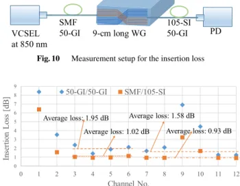
The insertion losses of the fabricated 3-D shuffling poly- mer waveguide, which are the combination of the coupling, bending and propagation losses, are measured. The mea- surement setup is schematically shown in Fig. 10. A VCSEL emitting at 850-nm wavelength is used as the light source, and for the launch/detection probes, two different combi- nations are employed: an SMF/105-µm core SI (105-SI) MMF and 50-GI/50-GI. In the case of the SMF/105-SI con- dition, the coupling losses between the probe and waveguide at both ends are minimized. Hence, the observed insertion losses could be regarded to be dominated by the propagation loss of the waveguide. In contrast, the insertion losses under the 50-GI/50-GI condition are potentially more realistic for on-board interconnects. The coupling losses at both ends of the waveguide with the probes, which are not negligible are involved in the insertion loss measured under the 50-GI/ 50-GI condition. Hence, from the insertion loss difference between these two conditions, the coupling loss between 50- GI and waveguide can roughly be estimated.
The length of the waveguide to be measured is 9 cm.
The insertion loss measurement results for the 3-D shuffling polymer waveguide are summarized in Fig. 11.
losses are 1.02 dB and 0.93 dB for the lower and upper level channels, respectively. The dependence of the loss on the channel number is attributed to the interim time difference over the channel numbers. We already confirmed in[22]
that the insertion loss of waveguides fabricated using the Mosquito method is sensitive to the interim time. On the one hand, in the case of upper level channels, Ch. 9 and Ch. 10 exhibit higher losses than the other channels: this is proba- bly due to the unwanted inclusion of dust particles. It is also found that the losses under the SMF/105-SI condition are lower than the losses under the 50-GI/50-GI condition con- sistently in all the channels. The insertion losses of the 3-D bent S-shaped polymer waveguides are discussed in more detail below.
3.2.2 3-D Bent S-shaped Core Polymer Waveguides The measurement setup for evaluating the insertion losses of the fabricated 3-dimensionally bent S-shaped polymer waveguides is the same as that shown in Fig. 10. The losses of lower and upper level channels are separately shown in Figs. 12 (A) and 12 (B), respectively.
From Fig. 12 (A), it is found that the insertion losses under the 50-GI/50-GI launch condition are consistently as low as 1.89 dB for an 8.4-cm long 3-D bent S-shaped lower 6-channel polymer waveguide. In contrast, under the SMF/105-SI launch condition, the loss is much lower than that of the 50-GI/50-GI launch condition, as the average loss is 0.97 dB, although all the channels contain both horizontal and vertical bent structures.
Moreover, from Fig. 12 (B), it is easily observed that, the insertion loss is consistently 2.41 dB on average un- der the 50-GI/50-GI launch condition for an 8.2-cm long 3-dimensionally bent S-shaped upper 6-channel waveguide.
However, under the SMF/105-SI launch condition, the loss is much lower than that of the 50-GI/50-GI launch condi- tion, as the average loss is 0.46 dB, although every chan- nel contains both horizontal and vertical bending structures.
In the fabricated waveguide, the desired cladding thickness was 1000µm, but the actual cladding thickness is approxi- mately 1220µm, as mentioned in Fig. 6 (B). So, the excess cladding thickness over the dispensed cores makes the core shape to be slightly elliptic, and therefore, the loss under the 50-GI/50-GI launch condition is slightly higher compared to the lower channel waveguide due to an excess coupling loss.
The larger coupling loss with 50-GI probe due to the elliptic core shape is also explained by the fact that the insertion loss under the SMF/105-SI condition in Fig. 12 (B) is remarkably low and even lower than those in Fig. 12 (A). In contrast, the insertion loss under the 50-GI/50-GI in Fig. 12 (B) is rather
Fig. 12
higher than that in Fig. 12 (A). We also compared the inser- tion losses of these 3-D bent S-shaped waveguides to the loss of straight waveguides. The insertion loss of straight waveguides is 1.31 dB under 50-GI/50-GI condition for a 5- cm long waveguide, which is comparable to the 3-D bent S-shaped waveguides with longer waveguide lengths.
3.2.3 Comparison of the Insertion Losses between 3-D Shuffling and 3-D Bent S-Shaped Polymer Waveg- uides
The average insertion losses for 3-dimensional shuffling waveguide are 1.95 dB and 1.58 dB for lower and upper channels, respectively under the 50-GI/50-GI launch con- dition, except for a couple of channels with accidentally high loss. Meanwhile, the losses for the corresponding S- shaped waveguides are 1.89 dB and 2.41 dB, respectively.
In the 3-D shuffling waveguide, the high losses in Ch. 9 and Ch. 10 could be caused by dust particles, whereas the high losses in Ch. 1 and Ch. 2 are attributed to overly long interim time causing the core diameter to increase and the numerical aperture to decrease. In the 3-D S-shaped waveguides, the interim time for Ch. 1 and Ch. 2 is not as long as that of the channels in the 3-D shuffling waveguide. So, the average insertion loss from Ch. 3 to Ch. 6 in Fig. 11 is compared to the average loss from Ch. 1 to 6 in Fig. 12 (A). Although the length of the shuffling waveguide is longer than that of the S-shaped waveguides, upper channels in the S-shaped wave- guide show slightly higher losses due to slightly elliptic core in Fig. 12 (B). Therefore, it is experimentally observed that the insertion losses for 3-dimensional shuffling waveguides
Fig. 13
are the same as the losses of 3-dimensionally bent S-shaped waveguides, and the over-crossing structure does not cause excess insertion losses. We would like to emphasize that the Mosquito method can successfully fabricate the low loss 3-dimensional shuffling structure of polymer optical waveg- uides with narrow interchannel pitch.
3.3 Crosstalk Analysis
The interchannel crosstalk in the 3-D shuffling polymer waveguide is one of the important optical properties. The interchannel crosstalk in the 3-D shuffling waveguide is ex- perimentally measured as follows: one channel of the wave- guide is launched using a 50-µm core GI-MMF probe, and then the output light from the cores in the 9-cm long shuf- fling waveguide is coupled to another 50-µm core GI-MMF probe to guide it to an optical power meter. Here, once the detection probe is aligned to the launched core, the detec- tion probe scans horizontally with a step of 1µm to align to the other cores in the lower and upper channel group on the output facet. Then, the output power is monitored at each position. It is obvious that the measured crosstalk in both levels, lower (Ch. 3 is launched) and upper (Ch. 9 is launched) channels of the 3-D shuffling waveguide, is low enough (lower than−30 dB) even to the nearest channels.
However, even though there are core bending and over- crossing structures, light leakage from the launched channel
waveguides with shuffling structures. However, from the re- sult in Fig. 11, we find that the insertion losses of Ch. 3 and Ch. 9 (the launched cores for the crosstalk measurement) are higher than other channels, which mean that there is a larger amount of light leakage from these two channels. Such an excess light leakage from Ch.3 and Ch.9 could cause the output power peaks from the nearest cores to the launched one. Actually, when Ch. 5 and Ch. 7 are launched for the crosstalk measurement, the drop-offs in power are observed from the nearest cores (Ch. 4, Ch. 6, and Ch. 8), similar to the general results observed in straight waveguides. The crosstalk in silica based single-mode multicore fibers is ex- pressed by mode coupling[23]. Meanwhile, in the 3-D shuf- fling multimode polymer waveguide, the interchannel pitch is 250µm, which is large enough to reduce the crosstalk due to mode coupling . Therefore, the cause of the interchannel crosstalk is mainly mode conversion, which could be likely be a result of high loss cores.
4. Conclusion
We successfully fabricated a unique structure, 3-dimensio- nal shuffling by over-crossing of the core groups in poly- mer optical waveguides applying the Mosquito method. The interchannel pitch of the fabricated waveguide is 250µm, and the upper channels cross over the lower channels in the cladding. The insertion losses are as low as 1.95 dB and 1.58 dB for lower and upper channel groups, respectively in a 9-cm long shuffling polymer waveguide at 850-nm wave- length, except for a couple of channels in which unwanted dust is present, even though both horizontally and verti- cally core-bending structures are involved. The insertion losses could further be decreased by completely removing the dust particles from the cladding monomer while coating the cladding monomer on the glass substrates. It is experi- mentally confirmed that there are no excess losses observed in shuffling waveguides, even compared to straight waveg- uides fabricated using the Mosquito method. The interchan- nel crosstalk in this waveguide is lower than−30 dB, which is low enough for parallel signal transmission. Therefore, this new type of 3-D shuffling polymer waveguide fabricated by the Mosquito method will improve the wiring density on- board optical interconnects.
References
[1] D.A.B. Miller, “Physical Reasons for Optical Interconnection,” Int.
J. Optoelectronics, vol.11, no.3, pp.155–168, 1997.
[5] B. Arimilli, R. Arimilli, V. Chung, S. Clark, W. Denzel, B. Drerup, T. Hoefler, J. Joyner, J. Lewis, J. Li, N. Ni, and R. Rajamony,
“The PERCS high-performance interconnect,” 2010 18th IEEE Symposium on High Performance Interconnects, California, USA, pp.75–82, Aug. 2010. DOI: 10.1109/HOTI.2010.16
[6] A.F. Benner, M. Ignatowski, J.A. Kash, D.M. Kuchta, and M.B.
Ritter, “Exploitation of optical interconnects in future server archi- tectures,” IBM J. Res. & Dev., vol.49, pp.755–775, 2005.
[7] R.C.A. Pitwon, K. Wang, J. Graham-Jones, I. Papakonstantinou, H.
Baghsiahi, B.J. Offrein, R. Dangel, D. Milward, and D.R. Selviah,
“FirstLight: Pluggable optical interconnect technologies for poly- meric electro-optical printed circuit boards in data centres,” J. Light- wave Technol., vol.30, no.21, pp.3316–3329, Aug. 2012. DOI:
10.1109/JLT.2012.2214764
[8] M. Usui, M. Hikita, T. Watanabe, M. Amano, S. Sugawara, S. Hayashida, and S. Imamura, “Low-loss passive polymer op- tical waveguides with high environmental stability,” J. Light- wave Technol., vol.14, no.10, pp.2338–2343, Oct. 1996. DOI:
10.1109/50.541226
[9] M. Hikita, R. Yoshimura, M. Usui, S. Tomaru, and S. Imamura,
“Polymeric optical waveguides for optical interconnections,” Thin Solid Films, vol.331, no.1-2, pp.303–308, Oct. 1998. DOI:
10.1016/S0040-6090(98)00935-3
[10] C. Choi, L. Lin, Y. Liu, J. Choi, L. Wang, D. Haas, J. Magera, and R.T. Chen, “Flexible optical waveguide film fabrications and opto- electronic devices integration for fully embedded board-level opti- cal interconnects,” J. Lightw. Technol., vol.22, no.9, pp.2168–2176, Sept. 2004. DOI: 10.1109/JLT.2004.833815
[11] F.E. Doany, C.L. Schow, B.G. Lee, R.A. Budd, C.W. Baks, C.K.
Tsang, J.U. Knickerbocker, R. Dangel, B. Chan, H. Lin, C. Carver, J. Haung, J. Berry, D. Bajkowski, F. Libsch, and J.A. Kash, “Ter- abit/s-class optical PCB links incorporating 360-Gb/s bidirectional 850 nm parallel optical transceivers,” J. Lightwave Technol., vol.30, no.4, pp.560–571, Feb. 2012. DOI: 10.1109/JLT.2011.2177244 [12] R. Kinoshita, K. Moriya, K. Choki, and T. Ishigure, “Polymer op-
tical waveguides with GI and W-shaped cores for high bandwidth density on-board interconnects,” J. Lightw. Technol., vol.31, no.24, pp.4004–4015, Dec. 2013. DOI: 10.1109/JLT.2013.2279791 [13] T. Ishigure and Y. Nitta, “Polymer optical waveguide with multiple
graded-index cores for on-board interconnects fabricated using soft- lithography,” Opt. Express, vol.18, no.13, pp.14191–14201, June 2010. DOI: https://doi.org/10.1364/OE.18.014191
[14] Y. Takeyoshi and T. Ishigure, “High-density 2×4 channel poly- mer optical waveguide with graded-index circular cores,” J. Light- wave Technol., vol.27, no.14, pp.2852–2861, July 2009. DOI:
10.1109/JLT.2009.2017385
[15] B.W. Swatowski, C.M. Amb, M.G. Hyer, R.S. John, and W.K.
Weidner, “Graded index silicone waveguides for high performance computing,” IEEE Optical Interconnects Conference, San Diego, USA, pp.133–134, May 2014. DOI: 10.1109/OIC.2014.6886115 [16] K. Kitazoe, R. Kinoshita, and A. Horimoto, “GI-core Polymer
Waveguide Based on Polynorbornene for Optical Interconnection,”
Proc. SPIE, vol.9753, pp.9753021–9753027, March 2016. DOI:
10.1117/12.2219405
[17] K. Soma and T. Ishigure, “Fabrication of a Graded-Index Circular- Core Polymer Parallel Optical Waveguide using a Microdispenser for a High-Density Optical Printed Circuit Board,” IEEE J. Se- lect. Topics Quantum Electron., vol.19, no.2, pp.3600310–3600310,
nol. Conf., Orlando, USA, pp.1042–1047, May 2014. DOI:
10.1109/ECTC.2014.6897416
[20] K. Yasuhara, F. Yu, and T. Ishigure, “Circular core single-mode polymer optical waveguide fabricated using the Mosquito method with low loss at 1310/1550 nm,” Optics Express, vol.25, no.4, pp.8524–8533, April 2017. DOI: http://doi.org/10.1364/OE.25.
008524
[21] Y. Saito, K. Fukagata, and T. Ishigure, “Low-loss polymer optical waveguides with graded-index perfect circular cores for on-board interconnection,” Proc. SPIE, San Francisco, USA, vol.9750, pp.9750051–9750056, March 2016. DOI: 10.1117/12.2212135 [22] R. Pitwon, K. Wang, A. Yamauchi, T. Ishigure, H. Schr¨oder,
M. Neitz, and M. Singh, “Competitive Evaluation of Planar Em- bedded Glass and Polymer Waveguides in Data Center Environ- ments,” Applied Sciences, vol.7, no.9, pp.940–956, Sept. 2017.
DOI: 10.3390/app7090940
[23] Y. Kokubun and M. Koshiba, “Novel multi-core fibers for mode division multiplexing: proposal and design principle,”
IEICE Electron. Express, vol.6, no.8, pp.522–528, 2009. DOI:
http://doi.org/10.1587/elex.6.522
Omar Faruk Rasel received the B.Sc.
and M.S. degrees in physics from Jahangirna- gar University, Bangladesh in 2006 and 2007, respectively. During August, 2011-November, 2013 and November, 2013 – September, 2016, he was working as a lecturer of Govt. Pio- neer Women College, Khulna and a Faculty of Physics Discipline, Khulna University, Khulna, Bangladesh, respectively. Currently, he is pur- suing a Ph.D. degree in material design science at Keio University, Yokohama, Japan. His cur- rent research interests include on-board optical interconnections realized with polymer optical waveguides. He has been a student member of IEEE since 2017.
Akira Yamauchi received the B.S. degree in applied physics and physico-informatics, and the M.S. degree in integrated design engineering from Keio University, Yokohama, Japan in 2015 and 2017, respectively. Currently, he is working for Softbank corp., Japan, as a network engineer.
waveguides. He has been a member of IEEE, OSA, JIEP, and JSAP. He has been a senior member of IEICE since 2017.