INVITED PAPER
Special Section on Cutting-Edge Technologies of Superconducting ElectronicsDevelopment of an Advanced Circuit Model for Superconducting Strip Line Detector Arrays
Ali BOZBEY†,††a), Yuma KITA††, Kyohei KAMIYA††,Nonmembers, Misaki KOZAKA††, Masamitsu TANAKA††,Members, Takekazu ISHIDA†††,Nonmember,andAkira FUJIMAKI††,Member
SUMMARY One of the fundamental problems in many-pixel detectors implemented in cryogenics environments is the number of bias and read-out wires. If one targets a megapixel range detector, number of wires should be significantly reduced. One possibility is that the detectors are serially connected and biased by using only one line and read-out is accomplished by on-chip circuitry. In addition to the number of pixels, the detectors should have fast response times, low dead times, high sensitivities, low inter-pixel crosstalk and ability to respond to simultaneous irradiations to individual pixels for practical purposes. We have developed an equivalent circuit model for a serially connected superconducting strip line detector (SSLD) array together with the read-out electronics. In the model we take into account the capacitive effects due to the ground plane under the de- tector, effects of the shunt resistors fabricated under the SSLD layer, low pass filters placed between the individual pixels that enable individual op- eration of each pixel and series resistors that prevents the DC bias current flowing to the read-out electronics as well as adjust the time constants of the inductive SSLD loop. We explain the results of investigation of the following parameters: Crosstalk between the neighbor pixels, response to simultaneous irradiation, dead times,L/Rtime constants, low pass filters, and integration with the SFQ front-end circuit. Based on the simulation re- sults, we show that SSLDs are promising devices for detecting a wide range of incident radiation such as neurons, X-rays and THz waves in many-pixel configurations.
key words: SSLD, kinetic inductance detectors, SFQ, superconductors, neutron detector
1. Introduction
Superconducting stripline detectors are promising devices especially for many-pixel applications up to megapixel[1]
resolutions when combined with single flux quantum (SFQ) read-out schemes[2]–[4]. It is possible to use only one bias point for an SSLD array and fabricate the detector together with the SFQ read-out electronics on the same chip in a monolithic configuration. Proof of concept devices have already been demonstrated[5],[6]and a feasibility for the megapixel scaling have been reported[1]. In addition, a recent study reports the electrothermal model for these de- vices[7]. As the performance parameters such as sensitivity, response time, and spatial resolution heavily depend on the physical and electrical parameters of the device, it is needed
Manuscript received October 20, 2015.
Manuscript revised January 6, 2016.
†The author is with TOBB University of Economics and Tech- nology, 06560, Ankara, Turkey.
††The authors are with Nagoya University, Nagoya-shi, 464–
8603 Japan.
†††The author is with Osaka Prefecture University, Sakai-shi, 599–8531 Japan.
a) E-mail: [email protected] DOI: 10.1587/transele.E99.C.676
to create an equivalent circuit model which is suitable for engineering the devices. In this paper, the input patterns for the simulation are based on a fiber coupled laser of the wavelength of 1550 nm which is used for the proof of con- cept experiments at the laboratory. However, SSLDs have the potential of being used for detecting photons and parti- cles in a wide range of spectrum. For instance, if proper ab- sorbing layers are deposited on top of the SSLDs, they can be used as a Neutron or X-ray detectors. If suitable anten- nas are coupled to individual SSLDs, THz imaging arrays can be fabricated.
One other important aspect of the SSLDs is that they have two modes of operation. Namely, inductive mode of operation and resistive mode of operation. If the SSLD is remains in the superconducting state response is generated based on current biased kinetic inductance detector prin- ciples[5]. However, if the incident radiation forces part of the SSLD to normal state, then the response is gener- ated based on bolometric[8] or superconducting nanowire single-photon detector[9]operation principles. Here we re- port the details of the model and simulation results that we have obtained for both modes of operation for various con- figurations.
2. Model Details
2.1 Detector Configuration and Circuit Model
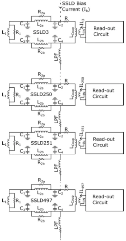
One pixel of an SSLD is composed of a superconducting stripline, a series resistance to the stripline, and a coupling coil. Stripline is the sensitive part of the detector, series re- sistance adjusts the time constant of the device as well as it converts the voltage signal to current, and coupling coil transfers the detector response to the read-out circuit. In the array configuration, low pass filters of the gain of about−3 dB at a frequency of 100 MHz are placed between pixels so that response generated at one SSLD does not propagate to neighbor SSLDs. This configuration is already reported elsewhere[1] and in Fig. 1 we report the proposed circuit model for that configuration. Each SSLD is a meander line with 0.7µm width, 50 nm thickness and 2 cm length. Dis- tance of the SSLD layer from the ground plane is 740 nm.
We have created a circuit model for 500 serially con- nected SSLDs for the configuration reported in[1]as shown in Fig. 1. In the figure, L1 is the irradiated part of the stripline where the voltage is generated according to the re- Copyright c2016 The Institute of Electronics, Information and Communication Engineers
Fig. 1 SSLD array configuration and circuit model.L1is the irradiated part of the stripline,L2aandL2brepresent the part of the SSLD where no radiation is exposed,C1-C4are the parasitic capacitance of the SSLDs,R2a
andR2bmodel the shunt resistances that are fabricated under the SSLDs.
LCOUPandLINrepresent the coupling coil to transfer the SSLD current to read-out circuit. LPF is a series L-R low pass filter circuit to prevent the crosstalk between pixels. IL3-IL497 represent the coupled current to the read-out circuit.
Fig. 2 (a) Simplified circuit model of the SSLD that shows the sources of L1 and L2 in the model. In this configuration, irradiation is assumed to be at the center andL2a=L2b. (b) shows the inductive mode and (c) shows the resistive mode models.
lation shown in Eq. (1) or Eq. (2) depending on the mode of operation. L2 = L2a+L2brepresents the part of the SSLD where no radiation is exposed.L1value is determined by the spot size of the laser, which is a circle of about 5µm diame- ter as shown in Fig. 2 (a). As the total length of the SSLD is 2 cm,L2/L1 is about 4000. L2a/L2b ratio is determined by
the location of the irradiation on the SSLD.
Different from similar models developed for super- conducting nanowire single photon detectors (SNSPD)[10], [11]we have taken into account the parasitic capacitance of the SSLDs (C1-C4) as the physical dimensions of the de- tectors are large and they have a ground plane underneath.
The reason for using a ground plane under the SSLDs is that as the dimensions of the stripline are in the order of cm, transmission-like behavior is needed to enable pulse prop- agation over the SSLD. Total capacitance of the SSLD is calculated as 1.950 pF and this value is distributed among C1-C4in proportional with theL2a/L2bratio during the sim- ulations. In Sects. 3.1–3.4, whereL2a/L2b =1,C1 =C3 = 0.325 pF andC2 =C4 =0.650 pF values are used. For the calculations in Sect. 3.5, whereL2a/L2b =100, capacitance values are scaled accordingly.
In addition, the shunt resistancesR2aandR2bmodel the resistances that are fabricated under the SSLDs to decrease the quality factor of the stripline configuration and dampen any possible oscillation in the loop.
Figure 2 shows the simplified models of the SSLD for inductive and resistive modes of operation. Generated re- sponses VL1 and VR1 due to incoming radiation for each mode are shown in Eqs. (1) and (2).
VL1(t)=IB×dL1(t)
dt (1)
VR1(t)=IB×R1(t) (2) Where,IBrepresents the DC bias current of the SSLD,L1(t) represents the change of the kinetic inductance of the SSLD due to the irradiation, and R1(t) represents the generated resistance of the irradiated part of the SSLD due to local heating. In both modes of operation, the generated voltage is converted to current by the series resistanceR and cou- pled to the read-out circuit by the coupling coil as shown in Fig. 1. In the simulation, we monitor the current at the sec- ondary side of the coil (LIN) which is directly connected to the read-out circuit shown in Fig. 4.
In order to determine the voltage input characteristics of the SSLD that simulate the actual response, we solved the simple model shown in Fig. 2 analytically in Laplace do- main. For various inductance transients, voltage character- istics are obtained as shown in Fig. 3. Throughout the paper, for inductive mode, we use the fastest input signal shown in Fig. 3 (b) that corresponds to 0.1 ns rise/fall times of induc- tance transient in order to show that the SSLDs can respond to such fast signals. For the positive side ofVR, we see that the voltage can track the inductance transient whereas for the negative side, recovery time is much slower. This value corresponds to theL2/Rtime constant of the loop, which is 10 nH/5Ω =2 ns.
2.2 Read-Out Circuit
Response of each SSLD pixel is transferred to the read- out electronics by using the coupling coil shown in Fig. 1.
Read-out circuit may be composed of a SQUID or quasi-one
Fig. 3 Generated voltage at the resistor of Fig. 2 (a) for various induc- tance transients for inductive mode. The result is based on a standard trans- fer function solution in the Laplace domain. Rise times of theL1transients are 0.1 ns, 1 ns, 1 ns, 10 ns respectively. For the simulation we usedL2=10 nH andR=5Ω.
Fig. 4 Read-out circuit for one SSLD pixel.IJ1=70µA,IJ1=110µA, IJ1=155µA,LIN=9.4 pH,L5=6.7 pH,L6=1.6 pH,L2,L3, andL4are parasitic inductances. RBand LBare the bias resistor and inductors respec- tively. Left side of the coupling coil belongs to the SSLD.kis the coupling coefficient betweenLINandLCOUP. CLK is the DFFe clock pulse. QOS is formed by theJ1-L4-J2loop. DFFe cell is used from the CONNECT cell library.
junction SQUID (QOS)[12]that gives a logic “1” output if the coupled current is higher than a predetermined thresh- old with the arrival of a sampling clock. In the paper we report the simulation results of a QOS based read-out cir- cuit. In this design, different from conventional QOS cir- cuits[12],[13]we utilized a clock-free QOS (CF-QOS) that oscillates with the arrival of a coupled current. At the output of the CF-QOS, a delay flip flop (DFF) circuit is connected so that any single flux quantum (SFQ) pulse that is gener- ated at the CF-QOS is latched. DFFe cell was used from the CONNECT cell library[14]that allows inputting consecu- tive SFQ pulses before DFFe clock pulse (CLK) is triggered as shown in Fig. 4. The reason for using such a configu- ration is that it simplifies the digital processing circuit but more importantly, the sampling clock may be much lower than the duration of the response especially at the inductive mode of operation. Even if the inductive response duration is much shorter than the clock period, since the SFQ pulse is latched at DFFe, with the arrival of a slower clock output
Fig. 5 Effect of theL/Rtime constant of the SSLD loop under induc- tive mode of operation. SSLD3-SSLD497have 1, 5, 20, and 50Ωseries resistances respectively.
can be obtained.
2.3 Resistive and Inductive Modes of Operation
SSLDs have two modes of operation, namely, inductive mode and resistive mode. If the SSLD is biased much lower than the critical current of the superconducting stripline or if the incoming radiation energy and/or intensity is low then local heating is not sufficient to have the stripline to switch to normal state. Then the stripline remains in the super- conducting state but the kinetic inductance changes due to broken cooper pairs[15]. In this mode of operation, it is assumed that the response at the SSLD is generated due to the change in the kinetic inductance of the detector which generates a voltage signal proportional todL/dtas shown in Eq. (1). This behavior is previously investigated and named as current biased kinetic inductance detector (CB-KID)[6].
If the SSLD is biased close to the critical current of the stripline, then an incoming radiation causes part of SSLD switch to the normal state and change of resistance trans- lates to a voltage signal under constant bias current with a relation shown in Eq. (2). The characteristics of this mode is similar to a superconducting nanowire single photon detec- tor (SNSPD)[9]or transition edge sensors (TES)[8]. Even though the output characteristics and read-out scheme for both modes of operation are similar, signal durations and shapes are different as shown in Figs. 5 and 6. Details of the inductive mode input has been explained in Sect. 2.1. For
Fig. 6 Effect of theL/Rtime constant of the SSLD loop under resistive mode of operation. SSLD3-SSLD497have 1, 5, 20, and 50Ωseries resis- tances respectively.
the resistive mode of operation input pattern, we assume that SSLD tracks the input pulse characteristics of our laser with 1 ns rise/fall times. Hence, inductive response duration is generally much shorter than that of resistive response. One thing to note is that, SSLD biasing or read-out scheme is the same for both modes of operation and it is not critical to force the SSLD array to operate in one mode of operation as long as the timings and signal amplitudes are in acceptable range.
3. Simulation Results
We have simulated the circuit shown in Fig. 1 by exciting four of the SSLD pixels out of 500 and observed the re- sponses of excited pixels as well as neighbor pixels. We used Jsim simulator[16]for all the simulations. In all the simulations, we applied triangular input to simulate induc- tive mode of operation, similar to the measurement results of [6], and square input to simulate the resistive mode of operation similar to the optical source that we use in our experiments, 1550 nm wavelength laser with 1 ns rise/fall times and 5ns duration time.
3.1 L/RTime Constant of the SSLD Pixel
L/Rtime constant of the stripline affects the response time and output amplitude of the SSLD directly. To see the effect of the L/R time constant of the SSLD loop, we kept the
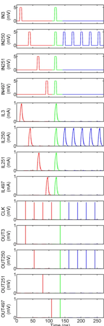
Fig. 7 Demonstration of the crosstalk (0-25ns), simultaneous radiation (30-35ns), and repetition rate (35-65ns) for inductive mode of operation.
IN3,IN250, IN251, andIN497 show the input for 3rd, 250th, 251st, and 497thSSLDs.IL3-IL497show the current in the coupling coil of the SSLD, OUT3-OUT497show the output of the respective SFQ front-end.
inductance of the stripline as 10 nH and changed the series resistance R from 1Ωto 50Ω. As shown in Figs. 5 and 6 we see that as R is increased, response speed of the SSLD increases due to the L/Rtime constant of the SSLD loop.
In this case, the amount of the coupled current (IL3-IL497) decreases due to Ohms’s lawI = V/I. It should be noted that SSLD voltage response is given by (1) or (2), which is constant for a given SSLD and incident radiation. We plan to read-out the response of the SSLDs with a QOS comparator circuit and the coupled current should be greater than the threshold value and gray-zone width of the comparator[12].
For this configuration we considered that best compromise between speed and coupled current magnitude is using R= 5 Ωin terms of speed and coupled current magnitude and used this value for the rest of the simulations.
Fig. 8 Demonstration of the crosstalk (0-125ns), simultaneous radiation (130-150 ns), and repetition rate (150-250 ns) for resistive mode of opera- tion.IN3,IN250,IN251, andIN497show the input for 3rd, 250th, 251st, and 497thSSLDs.IL3-IL497show the current in the coupling coil of the SSLD, OUT3-OUT497show the output of the respective SFQ front-end.
3.2 Inter-Pixel Crosstalk
One of the important aspects of a multi-pixel detector con- figuration is that the radiation falling on one of the pixels should not generate output at the neighbor pixels and read- out circuitry. As we placed low pass filters between the SSLDs, response generated at one of the pixels cannot prop- agate to the neighbor pixels and all the signal is directed to- wards the read-out circuit. This is shown in Figs. 7 and 8 in the duration of 0-25 ns and 0-125 ns intervals respectively.
In the figures,IN3-IN497represent the input voltagesVL1or VR1 of Fig. 2 for SSLD3-SSLD497 respectively. As shown in the figures, when the pixels 3, 250, 251, and 497 are ir- radiated at different times (IN3-IN497), neither any current
is coupled to the coupling coils of other pixels (IL3-IL497) nor is any response generated at the read-out circuit (OUT3- OUT497). Current is coupled only to the corresponding coil and only that read-out circuit gives output. For instance, when SSLD250is excited, current is coupled toLIN250and SFQ output is generated atOUT250only.
3.3 Response to Simultaneous Radiation
When the pixels are irradiated simultaneously, the response should not be affected from neighbor pixels irradiation. This is important as in an actual system photons can fall onto the pixels randomly and under such circumstances, individ- ual pixels should be able to operate independent from each other. To test this effect we have excited all the pixels at 30 ns for inductive mode and at 140 ns for resistive mode as shown in Figs. 7 and 8 respectively. When we observe the outputs as shown in the figures, coupled current and SFQ outputs operate as expected. From this result we can say that such a configuration is suitable for an imaging applica- tion.
3.4 Interval between Inputs and Dead-Time of the SSLD One of the circuit parameters that affects the maximum rep- etition rate of the incoming signal is theL/Rtime constant of the SSLD. As the designed SSLDs have 10 nH induc- tance and 5Ωresistance,L/Rtime constants of the SSLD loops are 2 ns. We have supplied input patterns to 250th SSLD and observed the output. For the inductive mode of operation repetition period is 5 ns and for resistive mode of operation, repetition period is 20 ns as the input pattern du- ration is already higher than 5 ns. As shown in Figs. 7 and 8 at 30-65 ns and 150-250 ns intervals, coupled current and SFQ output operates correctly at a repetition rate of 5 ns and 20ns respectively.
3.5 Position Dependence of the Radiation at the Stripline For the simulations in this part, we assumed that irradiation occurs at two edges of the SSLD as shown in Fig. 9. As the laser spot moves on the SSLD,L2a/L2bratio is changed whileL2a+L2b =L2remains constant. Figure 9 (a) shows the case of L2a/L2b = 0.01 and Fig. 9 (b) shows the case of L2a/L2b = 100. Figures 10 and 11 show the results for L2a/L2b =0.01 (IN250) andL2a/L2b =100 (IN251) respec- tively which correspond to irradiations at the two edges of the SSLDs. As shown in Figs. 10 and 11, regardless of the position of illumination SSLD output is as expected. Hence, we can deduce that this configuration is suitable for using the addressing scheme proposed in[1].
4. Conclusion
In this work, we have developed an advanced model to explain and predict different behaviors of superconducting stripline detectors both in inductive and resistive modes of
Fig. 9 Illustration of the radiation position effect on the circuit parame- ters of the model. (a) shows the case ofL2a/L2b=0.01 and (b) shows the case ofL2a/L2b =100. Figures are not to scale and show only the induc- tances for simplicity. Shunt resistors and parasitic capacitors of the SSLDs are scaled accordingly during simulation.
Fig. 10 Effect of the radiation at various positions of the SSLD pixel for the inductive mode of operation. 250thpixel is radiated at the position L2a/L2b=0.01 and 251stpixel is radiated at the positionL2a/L2b=100.
operation. We have shown that proposed configuration is suitable for crosstalk-free operation at low dead-times with the capability of single flux quantum logic read-out that will allow us to develop megapixel resolution imaging array. We anticipate that SSLDs have the potential of being used for detecting photons and particles in a wide range of spectrum if proper absorber layer and/or antennas are coupled to the detectors. With the use of advanced models similar to this paper, it will be possible to engineer the device structures for speed, number of pixels, and sensitivity.
Fig. 11 Effect of the radiation at various positions of the SSLD pixel for the resistive mode of operation. 250thpixel is radiated at the position L2a/L2b=0.01 and 251stpixel is radiated at the positionL2a/L2b=100.
Acknowledgments
This work is partially supported by TUBITAK with the project number 114E099 and JSPS KAKENHI with the grant number 23226019.
References
[1] T. Ishida, N. Yoshioka, Y. Narukami, H. Shishido, S. Miyajima, A.
Fujimaki, S. Miki, Z. Wang, and M. Hidaka, “Toward mega-pixel neutron imager using current-biased kinetic inductance detectors of Nb nanowires with 10B converter,” J. Low Temp. Phys., vol.176, no.3-4, pp.216–221, Aug. 2014.
[2] H. Terai, S. Miki, and Z. Wang, “Readout electronics us- ing single-flux-quantum circuit technology for superconducting single-photon detector array,” IEEE Trans. Appl. Supercond., vol.19, no.3, pp.350–353, June 2009.
[3] A. Bozbey, S. Miyajima, H. Akaike, and A. Fujimaki,
“Single-flux-quantum circuit based readout system for detector ar- rays by using time to digital conversion,” IEEE Trans. Appl. Super- cond., vol.19, no.3, pp.509–513, June 2009.
[4] H. Terai, S. Miki, T. Yamashita, K. Makise, and Z. Wang, “Demon- stration of single-flux-quantum readout operation for supercon- ducting single-photon detectors,” Appl. Phys. Lett., vol.97, no.11, 112510, Sept. 2010.
[5] N. Yoshioka, Y. Narukami, S. Miyajima, H. Shishido, A. Fujimaki, S. Miki, Z. Wang, and T. Ishida, “Four-channel current-biased ki- netic inductance detectors using MgB2nanowires for sensing pulsed laser irradiation,” J. Low Temp. Phys., vol.173, no.3-4, pp.273–278, 2014.
[6] N. Yoshioka, I. Yagi, H. Shishido, T. Yotsuya, S. Miyajima, A.
Fujimaki, S. Miki, Z. Wang, and T. Ishida, “Current-biased kinetic inductance detector using MgB2nanowires for detecting neutrons,”
IEEE Trans. Appl. Supercond., vol.23, no.3, 2400604, June 2013.
[7] C.N. Thomas, S. Withington, and D.J. Goldie, “Electrothermal model of kinetic inductance detectors,” Supercond. Sci. Technol., vol.28, no.4, 045012, April 2015.
[8] K.D. Irwin and G.C. Hilton, “Transition-edge sensors,” in Cryogenic Particle Detection, C. Enss, ed., Topics in Applied Physics, vol.99, pp.63–150, Springer Berlin Heidelberg, 2005.
[9] C.M. Natarajan, M.G. Tanner, and R.H. Hadfield, “Superconducting nanowire single-photon detectors: Physics and applications,” Super- cond. Sci. Technol., vol.25, no.6, 063001, June 2012.
[10] S. Jahanmirinejad and A. Fiore, “Proposal for a superconducting photon number resolving detector with large dynamic range,” Opt.
Express, vol.20, no.5, pp.5017–5028, Feb. 2012.
[11] S. Jahanmirinejad, G. Frucci, F. Mattioli, D. Sahin, A. Gaggero, R. Leoni, and A. Fiore, “Photon-number resolving detector based on a series array of superconducting nanowires,” Appl. Phys. Lett., vol.101, no.7, 072602, Aug. 2012.
[12] A. Bozbey, S. Miyajima, T. Ortlepp, and A. Fujimaki, “Design and circuit analysis of quasi-one junction SQUID comparators for low temperature detector array read-out,” J. Supercond. Nov. Magn., vol.24, no.1, pp.1065–1069, 2011.
[13] H. Ko and T. van Duzer, “A new high-speed periodic-threshold com- parator for use in a Josephson A/D converter,” IEEE J. Solid-State Circuits, vol.23, no.4, pp.1017–1021, 1988.
[14] S. Yorozu, Y. Kameda, H. Terai, A. Fujimaki, T. Yamada, and S.
Tahara, “A single flux quantum standard logic cell library,” Phys. C Supercond., vol.378-381, pp.1471–1474, 2002.
[15] P.K. Day, H.G. LeDuc, B.A. Mazin, A. Vayonakis, and J.
Zmuidzinas, “A broadband superconducting detector suitable for use in large arrays,” Nature, vol.425, no.6960, pp.817–821, Oct. 2003.
[16] E.S. Fang and T. van Duzer, “A Josephson integrated circuit simula- tor (JSIM) for superconductive electronics application,” Ext. Abstr.
2nd ISEC Tokyo Jpn., pp.407–410, 1989.
Ali Bozbey received the B.S., M.S., and Ph.D. degrees in electrical and electronics engineering from Bilkent University, Ankara, Turkey, in 2001, 2003, and 2006, respectively.
In 2002, he was a Guest Researcher with the J¨ulich Research Center, J¨ulich, Germany, and in 2007, he was a Postdoctoral Researcher with Nagoya University, Nagoya, Japan. Since 2008, he has been with the Department of Electrical and Electronics Engineering, TOBB University of Economics and Technology, Ankara, Turkey.
Yuma Kita received the B.E. and M.E. from Nagoya University, Nagoya, Japan in 2013 and 2015 respectively. His research interests include superconducting digital circuits and supercon- ducting detectors.
Kyohei Kamiya received the B.E. from Na- goya University, Nagoya, Japan in 2015. His research interests are superconducting detectors and systems.
Misaki Kozaka received the B.E. from Na- goya University, Nagoya, Japan in 2014. His re- search interests include superconducting digital circuits and applications.
Masamitsu Tanaka received the M.E.
and Ph.D. degrees in electronics and informa- tion electronics from Nagoya University, Na- goya, Japan, in 2003 and 2006, respectively. He was a JSPS Research Fellow from 2005 to 2007.
He joined Department of Information Engineer- ing, Nagoya University in 2007, and moved to Department of Quantum Engineering in 2010, where he is currently a designated lecturer. In 2011 he was a research scholar at the University of California, Berkeley, CA, USA. His research interests include the ultra-fast/energy-efficient computing using RSFQ cir- cuits and logic design methodologies.
Takekazu Ishida received the B.E. from Tohoku University, Sendai, Japan, in 1976. He received the M.E. and Ph.D. degrees from Kyoto University in 1978 and 1982, respectively. He has been working on material properties of su- perconductors for years. He proposed a new idea to produce a neutron detector using a new superconductor MgB2in 2001. He is currently a professor of Department of Physics and Elec- tronics at Osaka Prefecture University. His re- search interests are nanofabrication of supercon- ductor, its potential application as superconducting devices and magnetic properties of anisotropic superconductors.
Akira Fujimaki received his B.E, M.E., and Dr. Eng. degrees from Tohoku University in 1982, 1984, and 1987, respectively. He was a Visiting Assistant Research Engineer at the Uni- versity of California, Berkeley, in 1987. Since 1988, he has been working on superconduc- tor devices and circuits at the School of En- gineering, Nagoya University, Nagoya, Japan, where he is currently a professor. His current re- search interests include single-flux-quantum cir- cuits and their applications based on low- and high-temperature superconductors.