INVITED PAPER
Special Section on Award-winning PapersPhysical Fault Detection and Recovery Methods for System-LSI Loaded FPGA-IP Core
Motoki AMAGASAKI†a),Member, Yuki NISHITANI†, Kazuki INOUE†,Nonmembers, Masahiro IIDA†, Morihiro KUGA††,Members,andToshinori SUEYOSHI††,Fellow
SUMMARY Fault tolerance is an important feature for the system LSIs used in reliability-critical systems. Although redundancy techniques are generally used to provide fault tolerance, these techniques have signifi- cantly hardware costs. However, FPGAs can easily provide high reliability due to their reconfiguration ability. Even if faults occur, the implemented circuit can perform correctly by reconfiguring to a fault-free region of the FPGA. In this paper, we examine an FPGA-IP core loaded in SoC and in- troduce a fault-tolerant technology based on fault detection and recovery as a CAD-level approach. To detect fault position, we add a route to the manufacturing test method proposed in earlier research and identify fault areas. Furthermore, we perform fault recovery at the logic tile and multi- plexer levels using reconfiguration. The evaluation results for the FPGA-IP core loaded in the system LSI demonstrate that it was able to completely identify and avoid fault areas relative to the faults in the routing area.
key words: fault tolerant, fault recovery, FPGA-IP
1. Introduction
Fault recovery is extremely important in systems that require reliability, such as in-vehicle devices and medical equip- ment. Thus, most legacy systems maintain reliability using hardware-based redundancy. However, power consumption, area, and delay are the major drawbacks of this method.
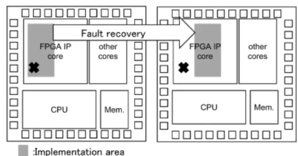
Considering this, the use of FPGAs (Field Programmable Gate Arrays), which use programmable features, promises to achieve fault recovery. In particular, because of the ex- tremely large number of restrictions on the implementation area, this method is extremely effective when an FPGA is loaded in the system LSI (Large Scale Integration) as an IP (Intellectual Property) core. As shown in Fig. 1, if a fault occurs within a circuit implementation area, a continuous operation to avoid the fault is possible using system recon- figuration. Therefore, there is no need to urgently replace the chip on which the fault exists within the FPGA-IP core.
This is particularly effective in environments where it is dif- ficult to replace chips, such as medical devices and remote areas.
To achieve a continuous operation, it is necessary to identify the fault location as quickly as possible. In addi-
Manuscript received November 7, 2016.
Manuscript revised December 26, 2016.
Manuscript publicized January 13, 2017.
†The authors are with the Graduate School of Science and Technology, Kumamoto University, Kumamoto-shi, 860–8555 Japan.
††The authors are with Faculty of Advanced Science and Tech- nology, Kumamoto University, Kumamoto-shi, 860–8555 Japan.
a) E-mail: [email protected] DOI: 10.1587/transinf.2016AWI0005
tion, extensive fault diagnosis is required to suppress the increased recovery time and performance loss due to fault recovery. The research on fault diagnosis and recovery in FPGAs can be largely classified into two types[1]; the first type deals with hardware-based approach. In this case, it is necessary to prepare redundant hardware resources in ad- vance as a spare location for circuit recovery; moreover, fault diagnostics and recovery are performed. Once a fault is discovered, diagnostics and recovery are performed quickly because fault recovery occurs in hardware. However, this process depends on hardware-based recovery mechanisms and lacks flexibility. In addition, it requires preparation of an alternative area; thus, the circuit’s area increases.
The second type deals with CAD (Computer Aided Design)-based approach. After identifying the fault loca- tion, configuration data that avoids the fault location is cre- ated. In this method, fault diagnosis is often adopted in switch units because no fault hardware resources are used.
Thus, this method is highly flexible and can handle all faults that can be rectified through placement or routing process.
Conversely, in the CAD-based approach, because it is neces- sary to perform replacement or rerouting, it becomes prob- lematic when there are limits on the time at which an appli- cation can be stopped. Consequently, numerous trade-offs occur when using fault diagnostics and recovery.
In this paper, we propose a fault detection and recov- ery approach that involves both CAD and a hardware aimed at stuck-at-faults caused by aging. After we mainly describe detail of CAD-based approach, hardware-based one is intro- duced based on[2]. The remainder of the present paper is or- ganized as follows. Related research is discussed in Sect. 2.
Section 3 describes CAD based fault tolerant method af- ter introducing our previous research on testing. In Sect. 4, we introduce hardware-based fault avoidance technique. Fi-
Fig. 1 Fault tolerance using FPGA reconfiguration.
Copyright c2017 The Institute of Electronics, Information and Communication Engineers
nally, conclusions are presented in Sect. 5.
2. Related Work
Several studies have investigated fault tolerance in FPGAs[1], [3]. In this paper, we consider situations in which fault tolerance is required owing to physical faults falling into the following categories.
1. Initial faults: Physical faults that occur during man- ufacturing of chips; e.g., stuck-at-faults, delay faults, and bridge faults.
2. Aging faults: These occur at a fixed ratio. There are also physical faults due to long-term operation, such as NBTI (Negative Bias Temperature Instability) and electro migration.
In addition, faults caused by cosmic radiation (i.e., single-event effects) include both temporary faults that can be recovered through a system reset and permanent faults in which transistors are broken. Previous fault-tolerant tech- nologies are essentially aimed at discrete FPGAs but include many parts that can be used in FPGA-IP cores. For initial faults, a redundant hardware resource is prepared as a spare resource for circuit diversion[4]–[7]. These faults are often detected using BIST (Built in Self Test) circuits embedded in advance. However, typically, these circuits only examine logical blocks.
There is a method that generates bit streams such that they avoid the fault area. In[8], based on the assumption that there is a high probability that unused LUTs (Look-up Tables) exist within the logic cluster, a method was proposed in which the circuits comprising fault LUTs were moved to an unused LUT. This is the most straightforward method of LUT fault recovery; however, fault diagnostics methods and performance after recovery process are not described in detail. In addition, relocatable bit stream technology has also been proposed[9]. Aging failure is also known as aging fault[10], and the test used for initial faults can be applied to stuck-at-faults caused by aging. For NBTI, other methods have been proposed[11].
In the case of single-event effects, the primary method involves masking software errors using TMR (Triple Mod- ular Redundant) and scrubbing[12],[13]. However, TMR has large area overhead; thus, a technology that uses DMR (Double Modular Redundant) and error coding check has been proposed[14]. Furthermore, there is a method that uses small configuration memory cells to reduce the soft error rate[15].
3. CAD-Level Approach
3.1 Policy
In fault diagnostics, fault recovery, and circuit performance, the circuit resources comprising an FPGA use three levels of granularity. Here, the coarseness of the granularity is di- vided into (A) tile levels, (B) block levels, and (C) multi- plexer levels.
Fig. 2 Relationship between the three types granularity.
(1) Tile level: Tiles are composed of LB (Logic Block), SB (Switch Block), and CB (Connection Block). As shown in Fig. 2 (a), the FPGA arranges tiles in an array, and resolu- tion is the lowest when dealing with faults at this level.
(2) Block level: As shown in Fig. 2 (b), the block level is used to deal with faults in LB, SB, or CB. In terms of resolution, this level is positioned between the tile level and the multiplexer level.
(3) MUX (Multiplexer) level: As shown in Fig. 2 (c), each block is configured as a group of MUX (switches); be- cause this level involves handling faults in multiplexer units, it has the highest resolution.
The time taken for specifying the fault location relative to the resolution is the shortest for the tile level and longest for the multiplexer level. In terms of fault recovery time, be- cause the tile level must place and route, significant recov- ery time is required; this leads to performance degradation.
Conversely, in the MUX level, only routes on MUX need to be changed; therefore, other wires do not need to be moved.
In other words, because only the signals that pass through the fault MUX are typically sufficient for incremental rout- ing, the recovery time and performance degradation can be kept to a minimum. However, if we have to treat faults on CB and LB parts, re-place and re-routing are needed.
In this section, we propose a fault diagnosis method that aims to reduce fault specification time at high diagnos- tic resolutions. We discuss the recovery time and recovery performance for an FPGA-IP core loaded on a system LSI.
We also consider the fault model for stuck-at-faults and tar- get the routing part, which is particularly difficult to test as a fault location. In addition, we discuss fault diagnostics time, recovery time, and circuit performance for an FPGA-IP core loaded on the system LSI. Fault diagnostics are performed using additional test patterns based on our previously pro- posed method[16]. Furthermore, for fault recovery, we have developed a tool at the tile and MUX levels; our tool is an improvement over the University of Toronto’s VPR[17]. In the FPGA-IP core, in contrast to a discrete-type FPGA, there are various circuit scales that depend on the design target.
Thus, scalability that depends on size is important.
3.2 Previous Work
This study uses a previously proposed architecture[16]for the target FPGA-IP core. This architecture, which aims to
improve the yield in manufacturing tests, has a simplified test design. In this subsection, we demonstrate the routing structure for test simplification and describe the SB level fault detection method.
3.2.1 Routing Structure for Test Simplification
The previous island-type FPGA has a structure that is com- plex to realize high programmability. In particular, the rout- ing part, which determines a route using configuration mem- ory, cannot directly use the ATPG (Automation Test Pattern Generation) tool. Thus, we propose a homogeneous archi- tecture[16] for a simple FPGA, as shown in Fig. 3. Al- though previous island-type FPGAs are configured using multiple tile structures, in this architecture, they are con- structed using a single tile. In addition, an aligner is used to simplify the connection. Furthermore, this architecture includes a TPG (Test Pattern Generator) with a test-pattern generation circuit to perform tests in an efficient manner, as shown in Fig. 4, and ORA (Output Response Analyzer) to
Fig. 3 Completely homogeneous tile architecture.
Fig. 4 IOB structure for testing.
compare the output within IOB. Furthermore, to reduce the test duration, it has a shift configuration structure in which the configuration information of the loaded circuits is stored in row units.
3.2.2 SB Test Patterns
The configuration pattern for detecting faults utilizes Wilton-type SB[18]regularity. Wilton-type SB routes can be classified as (A) straight line, (B) clockwise, or (C) coun- terclockwise (Fig. 5). For example, when configuring all SBs for a clockwise route, the routes are essentially config- ured as closed routes. However, there is a case where closed route is obstructed by passing through IOB. In closed-route SB, the LBs at the starting and end points are configured as TPG and ORA (Fig. 6), and the logical values output from TPG through the SB within the array and are stored in the FF of ORA. If it can be confirmed that the logic stored in ORA and the logic generated by TPG are the same, it can also be confirmed that there is no stuck-at-fault on the target route. Furthermore, where the route is not a closed one, a fault diagnostic is performed by the TPG and ORA within IOB. Since FF in ORA is scan type FF, the value of ORA is obtained through scan path. Here, the most advantageous feature is that all routes can be tested independently. Fig- ure 6 shows an example of a clockwise configuration route.
Fig. 5 Three types of SB configuration.
Fig. 6 Configuration for clockwise paths.
The broken line shows a route on the SB, and the bold line shows an actual route. As the routes passing through one SB do not interfere with the others, as shown in this figure, all clockwise routes can be examined simultaneously. This is also applicable to both counterclockwise and straight-line routes.
Furthermore, since closed route is actually discon- nected by TPG and ORA as shown Fig. 6, an additional pat- tern is required to test this disconnected parts. This sim- ply involves changing the position of TPG and ORA on this closed route. Considering this, one straight line route, two types of clockwise routes, and two types of counter- clockwise routes, i.e., five types of fault detection routes, are required. These routes were examined, and it was dis- covered that they could be used to detect 100% of the faults on routing part. However, this screening test does not spec- ify fault locations.
3.3 Fault Diagnostics
Using the manufacturing test method with the five types of wiring routes described in Sect. 3.2, we can only determine whether there are faults or not within FPGA-IP. Thus, we added a test pattern to specify the fault location.
3.3.1 Proposed Diagnostic Method
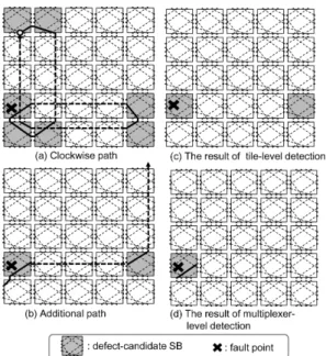
The previous research detected faults at the SB level. How- ever, as shown in Fig. 7 (a), multiple SBs can emerge as fault candidates, and it is not possible to specify the actual fault location. In addition, when performing recovery, it is not possible to use all SBs that are fault candidates. As shown in Fig. 7 (b), we use a new test route to perform fault diag- nostics. Next, as shown in Figs. 7 (c) and 7 (d), we search for overlapping locations in both search results and spec-
Fig. 7 Combining the paths to specify the faulty point.
ify the faults at the tile or MUX level. For the test support circuit, we use TPG and ORA as described in the previous section. With regard to ORA, to improve diagnostic accu- racy, we use the MUX type (shown in Fig. 8) rather than the legacy EXOR type. The signal Sel is a control signal input from the outer chip and is commonly input for each ORA.
3.3.2 Routes for Fault Detection
Two types of test routes were developed to specify the fault location. The first combines the right-sloped routes and di- rect line routes, as shown in Fig. 9 (a). The second com- bines the left-sloped routes and direct line routes, as shown in Fig. 9 (b). An example of the route configured in Fig. 9 (a) is shown in Fig. 10. The broken line represents the actual SB configuration patterns. As there are no closed routes in this pattern, TPG and ORA are used within IOB. For example,
Fig. 8 Modified output response analyzer.
Fig. 9 Additional SB configuration.
Fig. 10 Test pattern for right-up and orthogonal paths.
if we focus on the path indicated by the solid line, the signal output from the TPG within IOB passes through the solid- line and is stored in the ORA in IOB. As these routes do not cross, all routes in the broken line can be tested simultane- ously. Fault diagnostics are performed on the straight-line and left-sloped route test patterns in the same manner.
The case in which the direct-line and right-sloped routes are replaced in units related to the route shown in Fig. 10 is shown in Fig. 11. By replacing the SB configu- ration information stored in row units, a direct-sloped test can be performed on all tiles. The SB configuration time is reduced by changing the circuit configuration in row units;
thus, the shift configuration function[16], which reconfig- ures one line of the array using a shift operation, is used. As shown in Fig. 12, these compose the configuration path as a shift register and can control these in row units. Using the above-mentioned functions, the routes in Figs. 10 and 11 can
Fig. 11 Shifted test pattern.
Fig. 12 Structure of configuration path.
be changed easily. By combining the added routes and shift configuration, the ability to analyze faults in a short time can be improved. Note that this ability can also be tested using a method similar to that shown in Fig. 9 (b).
As these routes contain direct line routes, it is not necessary to independently execute the straight-line routes shown in Fig. 5. In this manner, fault detection is performed with six types of test routes, i.e., two types of clockwise routes, two types of counter-clockwise routes, a straight- line/left-sloped route, and a straight-line/right-sloped route.
As these routes will necessarily overlap the routes on SBs, it is possible to detect 100% of the faults on an SB. If the SB faults are identified, the fault tiles can also be specified. In addition, if the fault wire can be identified, the fault MUX can also be identified. In other words, using this method, it is possible to detect faults at the tile, block, and MUX levels.
3.3.3 Number of Cycles for Fault Diagnosis
The time required for fault diagnosisTdetect[cycle] is deter- mined by the number of full configuration (Nf ull) and the number of shift configurations (Nshi f t).
Tdetect=Tf ull·Nf ull+Tshi f t·Nshi f t (1) In [16], because the tests were performed using five types of routes, Nf ull = 5. Furthermore, in the proposed method, because the tests are performed with six types of routes for an SB, Nf ull = 6. In addition, as shift configu- ration is performed once for each straight-line/right-sloped route and straight-line/left-sloped route, Nshi f t = 2. Pro- vided that a Wilton-type SB is used, the above-mentioned parameters remain the same for any FPGA-IP core-array size. Tf ull is the time required to obtain the results using total reconfiguration from the scan path.
Tf ull=CFarray+CFiob+Tscan (2)
CFarrayrefers to the number of configuration memories for the FPGA array, andCFiob is the number of configura- tion memories for total IOB. Here, the FPGA size is defined as Narrayx×Narray y, where Narrayx is the number of row tiles andNarray y is the number of column tiles. Thus, the total number of tilesT Ntileis calculated as follows.
T Ntile=Narrayx·Narray y (3) Here,Tscanrepresents the time required for the FPGA- IP core scan, and Nf f lb andNf f iobexpress the number of FFs per LB and IOB, respectively, in the following formula.
Tscan=T Ntile·Nf f lb+2(Narrayx+Narray y)·Nf f iob (4) The number of cycles required for shift configuration is expressed as follows.
Tshi f t=CFarray
Narrayx + CFiob
2(Narray y+Narray y)+Tscan (5) Furthermore, if we consider the number of configura- tion memories per LB, CB, and SB asCFlb,CFcb, andCFsb,
respectively, the number of configuration memories for the FPGA array is given as follows.
CFarray=(CFlb+CFcb+CFsb)·T Ntile (6) Here, in terms of the channel widthW, if we consider the ratio of single lines and quad lines to beα : (1−α), the number of configuration memories per one SB,CFsb, is expressed as follows.
CFsb=CFmux sb·W 2
1−3
4(1−α)
·4 (7)
Here, CFmux sb refers to the number of configuration memories per MUX switch within an SB. The coefficientW2 is single-direction wire. Furthermore, as three-quarters of the quad lines are not input to the target SB, they are sub- tracted from the total number of lines. Then, the remainder is multiplied by 4 in consideration of up/down and left/right inputs. For example, ifCFmux sb = 3 bits and the single line : quad line ratio is=1 : 5,CFsb =9W4 . Thus, the effect of channel width on overall test time isO(W).
3.4 Fault Recovery
To recover the faults diagnosed in the previous subsection, the placement and routing tool VPR5.0[17]is added to the fault recovery function.
3.4.1 Placement
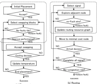
When diagnosing at the tile level, the LB within the fault tile cannot be used. Thus, it is necessary to recover the fault LB in the placement process. The placement flow of VPR is changed, as shown in Fig. 13 (a). The part of the broken line section determined as faulty has the coordinate information for the fault tiles in advance. Because VPR uses the simu- lated annealing method, a function is added to exclude the
Fig. 13 Replacement and routing flow.
fault tiles during initial placement and when swapping the logic module. The pseudo code for this algorithm is shown in Fig. 14. If the fault block for initial placement is selected on line 5, initial placement is redone until a block other than the fault block is selected. When the fault block is selected as the block destination on line 14, the placement is redone until a block other than the fault block is selected.
3.4.2 Routing
When recovering the tile and MUX levels, it is neces- sary to exclude the fault routes from the routing resource graph. Here, the VPR routing flow is changed as shown in Fig. 13 (b). The part of the broken line determined as faulty also contains fault tile coordinate information in advance, as in the case of routing. To prevent performance degradation due to recovery, instead of reconfiguring everything, routing is done incrementally; i.e., only the routes relevant to the fault location are changed. Thus, a change is made to the pathfinder[19], i.e., the VPR routing algorithm. The pseu- docode for this algorithm is shown in Fig. 15. Processing is performed to determine whether the node selected on line 21 is faulty. If the pathfinder were to select faulty wire, the routing process would fail at that point and routing would be performed for other routes.
3.5 Evaluation
The method used in[16]and the proposed method are com- pared in terms of fault diagnosis and recovery. This evalu- ation covers the tile and MUX levels. Next, the placement
Fig. 14 Pseudo-code in fault avoidable placement.
Fig. 15 Pseudo-code in fault avoidable routing.
Table 1 Architecture parameter.
Item Value
Array size 16×16
Logic cell 6-LUT
Cluster size 4
Number of LB input 12
SB type Wilton (Fs=3)
CB type normal (Fc=0.5)
Number of single line 8/channel Number of quad line 40/channel
Number of I/O pin 128
Number of configuration bits 136,896
and routing tool supporting fault recovery are used to eval- uate circuit performance and recovery time after fault re- covery. Finally, we discuss a trade-offbetween test time, performance, and recovery time.
3.5.1 Evaluation Conditions
The details of the architecture to be evaluated are shown in Table 1. The FPGA-IP core is a homogeneous architecture with an array size of 16×16. The number of LUTs loaded within a logical block is defined by the logical cluster size, which is set to 4. In this evaluation, a 65-nm CMOS stan- dard cell library is used, and the value synthesized with Syn- opsys Design CompilerY-2006.06-SP6-2 is used as a device
Table 2 Result of fault detection.
Previous[16] Propose
# of full configuration 5 6
# of shift configuration – 2
Test time (cycle) 798,992 975,278
Increase rate of test time – +22.0%
# of candidate fault tile (worst) 45 1
# of candidate fault tile (best) 4 1
# of candidate fault MUXe (worst) 144 1
# of candidate fault tile (best) 12 1
parameter. The fault model is stuck-at-fault, and the toggle coverage for the Cadence NC-Verilog06.20-s004 is handled as an observed value for the fault specification rate.
In this evaluation, a maximum of five faults occur in the routing part at any one location. Fault diagnosis is per- formed on the basis of the respective number of faults for 1,000 patterns at random locations. Furthermore, with the MCNC benchmark circuit[20]for evaluating the circuit per- formance, a placement and routing tool is used with the ABC mapper[21], T-VPack[19], and added recovery func- tions. The computer used in the simulation was an Intel Xeon X5680 with a 3.30 GHz processor and 48 GB mem- ory.
3.5.2 Fault Diagnosis
Table 2 shows the diagnosis results for a single fault. As the fault diagnosis capacity relies on the test route and the tests routes collected in ORA, both the best and worst values are shown. For the test method used in[16], because the five types of test routes described in Sect. 3.2 must be fully re- configured, the number of reconfigurations for the FPGA-IP core is five (Nf ull = 5). Furthermore, the number of clock cycles required at that time is 798,992, and the breakdown is 786,245 cycles (98.4%) for the full configuration and 11,528 cycles for scans (1.4%); the remaining 1,219 cycles (0.2%) are for control operations. However, initially, this method specifies only the existence of faults within the chips. Thus, the fault-level detection ability was low at the tile level, i.e., 4 for the best value and 44 for the worst value. Conversely, for the proposed method, because the six types of test cir- cuits discussed in Sect. 3.3 require full configuration and two shift configurations, the total number of full reconfig- urations for the FPGA-IP core is six (Nf ull = 6) and the shift configuration is two (Nshi f t =2). The number of clock cycles required at this time is 975,278, i.e., 943,494 cycles (96.7%) for the full configuration, 19,010 cycles (1.9%) for the shift configuration, and 11,528 cycles (1.2%) for scans.
The remaining 1,246 cycles (0.1%) are for control opera- tions. Although the test duration increased by 22.0%, we were able to perfectly recognize the fault location at both the tile and MUX levels.
Next, the fault diagnosis results in the case wherein faults are caused in a maximum of five locations are shown in Tables 3 and 4. Here, based on the injected fault position and the number of faults, the best, worst, and average values for 1,000 attempts are shown. For example, in a previous
Table 3 Candidates of detected faulty points (Previous).
# of defects tile level mux level
best worst ave. best worst ave.
1 9 45 23.5 24 144 57.6
2 13 88 40.5 46 288 123.7
3 23 110 54.1 85 324 168.9
4 35 167 83.0 123 564 247.6
5 83 183 94.8 157 642 290.2
Table 4 Candidates of detected faulty points (Proposed).
# of defects tile level mux level
best worst ave. best worst ave.
1 1 1 1.0 1 1 1.0
2 2 2 2.0 2 2 2.0
3 3 3 3.0 3 3 3.0
4 4 4 4.0 4 4 4.0
5 5 5 5.0 5 5 5.0
research, for five faults, an average of 94.8 at the tile level and 290.2 at the MUX level could be identified. Conversely, the proposed method was able to perfectly identify the sites with multiple fault locations at the tile and MUX levels.
3.5.3 Fault Recovery
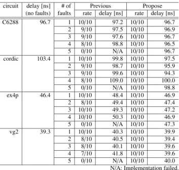
In the case of a maximum of five faults occurring at any location in the FPGA, we perform two types of fault diag- nosis: (1) using the previous research method and (2) using the proposed method. In addition, we perform fault recov- ery using the proposed tool. Four types of MCNC bench- mark circuits, “C6288”, “cordic”, “ex4p”, “vg2”, are used in the implementation. If a fault occurs in a position unre- lated to the implemented circuit, there is no need to perform recovery on that location specification. Therefore, this eval- uation only covers cases in which the implemented circuit was on a fault location. The delay in the critical path when performing fault recovery at the tile and MUX levels are shown in Tables 5 and 6, respectively. The first columns of these tables contain the names of the implemented circuits, the second columns contain the operating speed before re- covery, the third columns contain the embedded number of faults, and the fourth and fifth columns contain the recovery results of the previous and proposed methods, respectively.
Ten attempts are made using the route changed after the ini- tial placement; thus, “rate” is the number of successful re- coveries out of 10, and delay expresses the average value of these recoveries. In the tile recovery process performed in a previous study, reconfiguration failed, and when it did succeed, approximately 10% performance degradation was observed. The reason for this was a large number of fault tile candidates, which caused a lack of resources at the time of reconfiguration. Conversely, using the proposed method, al- though the performance degradation after recovering from the fault is approximately 2%, recovery is successful for all patterns. At the MUX level, for the previous detection method, the number of fault recoveries increase and perfor- mance degradation is limited to approximately 2%. Using
Table 5 Delays for tile-level avoidance (ten samples).
circuit delay [ns] # of Previous Propose (no faults) faults rate delay [ns] rate delay [ns]
C6288 96.7 1 7/10 99.9 10/10 95.9
2 1/10 99.4 10/10 94.8
3 0/10 N/A 10/10 94.1 4 0/10 N/A 10/10 96.1 5 0/10 N/A 10/10 95.5
cordic 103.4 1 6/10 108.2 10/10 100.8
2 0/10 126.0 10/10 102.0 3 0/10 N/A 10/10 104.0 4 0/10 N/A 10/10 104.0 5 0/10 N/A 10/10 108.0
ex4p 46.4 1 5/10 54.9 10/10 47.5
2 0/10 50.3 10/10 47.9
3 0/10 N/A 10/10 47.9
4 0/10 N/A 10/10 49.9 5 0/10 N/A 10/10 49.3
vg2 39.3 1 8/10 41.5 10/10 40.4
2 4/10 41.7 10/10 41.4
3 6/10 44.9 10/10 39.8
4 4/10 43.6 10/10 40.6
5 0/10 N/A 10/10 40.8 N/A: Implementation failed.
Table 6 Delays for MUX-level avoidance (ten samples).
circuit delay [ns] # of Previous Propose
(no faults) faults rate delay [ns] rate delay [ns]
C6288 96.7 1 10/10 97.2 10/10 96.7
2 9/10 97.5 10/10 96.9
3 9/10 97.6 10/10 96.7
4 8/10 98.8 10/10 96.5
5 0/10 N/A 10/10 96.7
cordic 103.4 1 10/10 99.8 10/10 97.5
2 9/10 98.7 10/10 95.9
3 9/10 99.6 10/10 94.3
4 8/10 109.0 10/10 100.0 5 0/10 N/A 10/10 98.8
ex4p 46.4 1 10/10 48.4 10/10 46.9
2 8/10 49.4 10/10 47.4
3 10/10 49.3 10/10 47.2 4 10/10 50.3 10/10 46.9 5 0/10 N/A 10/10 47.3
vg2 39.3 1 10/10 40.3 10/10 39.9
2 8/10 40.5 10/10 39.4
3 8/10 40.1 10/10 39.6
4 7/10 41.8 10/10 39.6
5 0/10 N/A 10/10 40.0 N/A: Implementation failed.
the proposed method, recovery is successful for all patterns and no degradation in operating speed is observed at the tile level.
Figure 16 shows the routing results for three faults in the ex4p benchmark. In Fig. 16 (a), the previous detection method is used and recovery is performed at the tile level.
Here, because 45 types of fault candidates are present, there is a lack of routing resources; consequently, fault recovery was fail. Figure 16 (b) shows the routing results when fault diagnosis and recovery are performed using the proposed method under the same conditions. Here, routing is done to avoid the fault tiles, and we observe that fault recovery was successful.
Fig. 16 Result of the ex4p benchmark circuit.
Table 7 Avoidance time [s].
circuit Tile MUX
(re-place&routing) (re-routing only)
C6288 3.102 0.432
cordic 4.654 1.206
ex4p 4.148 0.495
vg2 1.437 0.177
The recovery time when using a computer is shown in Table 7. At the MUX level, the fault recovery duration is, on an average, 84% shorter than that at the tile level. This is because although it is necessary to replace and route when recovering faults at the tile level, only reconfiguration is re- quired at the MUX level.
3.5.4 Discussion
We observe that when the previous fault detection method is used, compared with the proposed method, there is a ma- jor difference between the rerouting success rate at the tile and MUX levels. In particular, fault recovery at the tile level fails for many benchmark circuit implementations. It is con- sidered that this is due to the fact that when performing fault recovery at the tile level, none of the elements in the logical block can be used. Conversely, at the MUX level, recovery is performed only on the minimum number of fault areas;
thus, in comparison to the tile level, recovery has a higher degree of flexibility at the MUX level. However, although the number of recovery successes increases as a whole, fault recovery was failed in the case of five faults. In addition, using the proposed diagnostic method, fault detection and recovery are possible for both the tile and MUX levels, and very little performance degradation is observed. Further- more, we observe that in terms of recovery time, the fault time at the MUX level is shorter than that at the tile level.
Thus, at the tile level, the proposed method is superior to the previous method in terms of fault diagnosis/recovery at the MUX level relative to recovery time, recovery success rate, and overall performance.
Finally, in Fig. 17, we show the time required for fault diagnosis when the FGPA-IP core size and channel width fluctuate. In this evaluation, the number of test cycles with an array size of 16×16 and channel width of 48 is 1,123,018
Fig. 17 Relationship between total number of tiles and channel width.
(Table 2). Conversely, when the array size is 128×128 and the channel width is 192, the number of test cycles is 98,862,596. As described in Sect. 3.3.3, the test duration increases proportionately to channel width W, and when the test block cycle is set to 10 MHz, the test is completed within 1 sec.
4. Hardware-Level Approach
In Sect. 3, CAD-level fault recovery approach is introduced.
Conversely, we have developed FPGA architecture featur- ing high tolerance to physical errors for soft-IP-based pro- grammable logic design as a hardware-level fault recovery approach. The feature of the architecture is summarized in this section. More detail information and evaluation results can be obtained in[2].
4.1 Policy
In order to perform hardware-level fault recovery, the con- figuration data of an implemented circuit must be moved quickly to fault-free regions. Thus, we consider the follow- ing points: The first is fault recovery (avoidance) method with embedded spare modules. But, additional hardware module have to be kept to a minimum to ensure high cir- cuit performance. The second is design scalability. Scalable design technique is needed since target application require different array size. The third is automation of both fault de- tection and fault avoidance. To perform proper fault avoid- ance, it is important to detect the fault location. Thus, au- tomation of both fault detection and avoidance is desirable.
4.2 Detail Architecture
Figure 18 shows our FT-FPGA architecture. FT-FPGA is based on the homogeneous routing architecture in[16], which has a simple regular structure. In this architecture, the entire region is divided into several groups of tiles re- ferred to as tile arrays (TAs). Each TA includes spare tiles, and fault avoidance is performed in individual TAs.
A single column of spare tiles is placed to the right of the main array. In the absence of faults, a circuit is con- figured with normal tiles and the spare tiles are not used
Fig. 18 FT-FPGA overview. This structure consists of 2×2 TAs composed of 3×3 normal tiles and a column of one spare tiles.
Fig. 19 Fault avoidance by shifting columns of tiles.
(Fig. 19(a)). If a fault occurs, part of the implemented cir- cuit is moved to fault-free tiles to the right of the column containing faulty tiles (Fig. 19 (b)). However, moving cir- cuits causes connection mismatches between TAs. To ad- dress this mismatches, we implement TA interfaces, which are constructed as selectors between TAs, to update the con- nections.
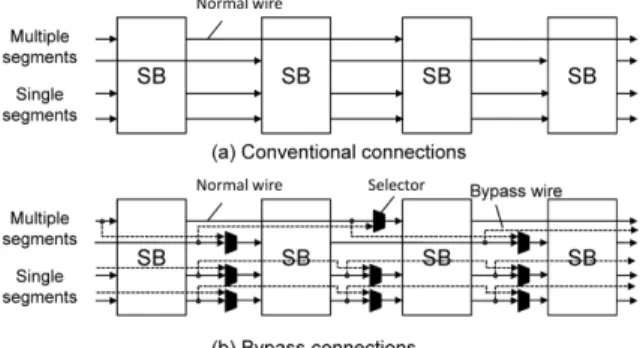
Connections between tiles must be rerouted after im- plementing fault avoidance. Therefore, we introduce by- pass wires. Figure 20 (a) shows conventional wire segments between SBs. In contrast, we implement bypass wires as shown in Fig. 20 (b). All segments have bypass wires, each of which is connected to a selector. When performing fault avoidance, these selectors switch the connections between SBs so as to skip faulty tiles. Moreover, all connections within TA are composed of single-wire segments, and the connections between TAs are composed of both single-wire and multiple-wire segments. Single-wire segments are used to connect neighboring TAs as well as individual tiles, and multiple-wire segments connect distant TAs. Since fault avoidance is implemented within individual TAs, multiple-
Fig. 20 Segment connections using bypass wires.
Table 8 Characteristics of the manufactured TEG chip.
Item Value
Array size (tiles) 20×20
Tile array size (tile array) 5×5
Tile array structure 4×4 normal tiles+4×1 spare tile
Logic clusters 4
# of LB inputs 10
SB structure Wilton (Fs=3)
CB structure normal (Fc=0.5)
# of single lines in tile array 14/unidirectional channel
# of IO pins 208
# of FFs for conf. mem. (bit) 205,520
Chip size (mm) 12mm2(3.46mm)
Process 65nm (TSMC)
wire segments do not have bypass wires.
4.3 Chip Design
In order to estimate area impact, we design an actual FT-FPGA TEG (Test-element Group) chip using a 65-nm TSMC standard cell library. Table 8 shows the characteris- tics of the TEG chip, and Fig. 21 (a) shows a top view of the chip layout. The TEG chip has a 5×5 TAs with 4×4 nor- mal tiles and 4×1 spare tiles. The total number of normal and spare tiles is 400 (20×20 tiles) and 100, respectively.
Moreover, the total number of configuration memory bits is 205,520, and total die area is 12mm2 (3.46mm×3.46mm).
Note that we utilize scan type FFs as a configuration mem- ory cells.
Figure 21 (b) shows the layout of the tile array; its area is 0.34 mm2. Figures 21 (c) and (d) shows the layout of normal and spare tiles. Since spare tiles do not have con- figuration memory bits, their area is about one-seventh that of a normal tile. The total spare tile area is only 4.3% of the total die area. All functions that include normal opera- tion and fault detection/avoidance operations are examined by downloading the bitstream.
5. Conclusion
In this paper, we introduce a fault detection and recovery approach that involves both CAD and an hardware aimed at aging stuck-at-faults. In the case of CAD-based approach, we proposed a fault diagnosis method for the routing part
Fig. 21 Chip layout.
of an FPGA-IP core and developed a tool for placement and routing to perform fault recovery. Using the proposed method, we confirmed that a highly efficient fault diagno- sis could be achieved using six test configurations. Further- more, we experimentally confirmed that, at both the tile and MUX levels, fault detection and recovery were performed efficiently. In addition, in terms of the operating speed, fault recovery at the MUX level caused no performance degrada- tion.
Next, we introduce hardware-based fault recovery technique and an actual TEG chip design. The key features of this architecture are spare modules and bypass wires for fault avoidance. In the case of hardware-based approach, the system can continue operating when a fault occurs because of its capability to perform rapid fault avoidance. By using above two approaches properly, designer can obtain optimal design according to their constrains.
Acknowledgements
This work is supported by VLSI Design and Education Cen- ter (VDEC), the University of Tokyo in collaboration with Synopsys, Inc. and Cadence Design Systems, Inc.
References
[1] J.A. Cheatham, J.M. Emmert, and S. Baumgart, “A survey of fault
tolerant methodologies for FPGAs,” ACM Trans. Design Automa- tion of Electronic Systems (TODAES), vol.11, no.2, pp.501–533, 2006.
[2] M. Amagasaki, Q. Zhao, M. Iida, M. Kuga, and T. Sueyoshi,
“Fault-tolerant FPGA: Architectures and design for programmable logic intellectual property core in SoC,” IEICE Trans. Inf. & Syst., vol.E98-D, no.2, pp.252–261, Feb. 2015.
[3] E. Stott, P. Sedcole, and P.Y.K. Cheung, “Fault tolerant methods for reliability in FPGAs,” Proc. International Conference on Field Pro- grammable Logic and Applications, pp.415–420, Sept. 2008, [4] A. Doumar and H. Ito, “Defect and fault tolerance SRAM-based
FPGAs by shifting the configuration data,” IEICE Trans. Inf. &
Syst., vol.E83-D, no.5, pp.1104–1115, May 2000.
[5] J.L. Kelly and P.A. Ivey, “A novel approach to defect tolerant design for SRAM based FPGAs,” Proc. ACM International Workshop on Field Programmable Gate Arrays, pp.1–11, Feb. 1994.
[6] S. Durand and C. Piguet, “FPGA with selfrepair capabilities,” Proc.
ACM International Workshop on Field Programmable Gate Arrays, pp.1–6, Feb. 1994.
[7] N. Howard, A. Tyrrell, and N. Allinson, “The yield enhancement of field-programmable gate arrays,” IEEE Trans. Very Large Scale Integr. (VLSI) Syst., vol.2, no.1, pp.115–123, 1994.
[8] V. Lakamraju and R. Tessier, “Tolerating operational faults in cluster-based FPGAs,” Proc. ACM/SIGDA International Sympo- sium on Field Programmable Gate Arrays, pp.187–194, 2000.
[9] F. Lima, L. Carro, and R. Reis, “Designing fault tolerant systems into SRAM-based FPGAs,” Proc. 40th Annual Design Automation Conference, pp.650–655, 2003.
[10] S. Srinivasan, P. Mangalagiri, Y. Xie, N. Vijaykrishnan, and K.
Sarpatwari, “FLAW: FPGA lifetime awareness,” Proc. 43th Annual Design Automation Conference, pp.630–635, 2006.
[11] M. Yabuuchi and K. Kobayashi, “NBTI-induced delay degradation analysis of FPGA routing structures,” IPSJ Trans. System LSI De- sign Methodology, vol.5, pp.143–149, 2012.
[12] K. Kyiakoulakos and D. Pnevmatikatos, “A novel SRAM-based FPGA architecture for efficient TMR fault tolerance support,” Proc.
International Conference on Field Programmable Logic and Appli- cations (FPL), pp.193–198, Sept. 2009.
[13] C. Bolchini, A. Miele, and M.D. Satambrogio, “TMR and partial dynamic reconfiguration to mitigate SEU faults in FPGAs,” Proc.
IEEE International Symposium on Defect and Fault-Tolerance in VLSI Systems (DFT), pp.87–95, Sept. 2007.
[14] I. Kuon, R. Tessier, and J. Rose, “FPGA architecture: Survey and challenges,” Foundations and Trends in Electronic Design Automa- tion, vol.2, no.2, pp.135–253, Feb. 2007.
[15] Q. Zhao, Y. Ichinomiya, Y. Okamoto, M. Amagasaki, M. Iida, and T. Sueyoshi, “A robust reconfigurable logic device based on less configuration memory logic cell,” Proc. International Conference on Field-Programmable Technology (FPT), pp.162–169, Dec. 2010.
[16] K. Inoue, M. Koga, M. Amagasaki, M. Iida, Y. Ichida, M. Saji, J. Iida, and T. Sueyoshi, “An easily testable routing architecture and prototype chip,” IEICE Trans. Inf. & Syst., vol.E95-D, no.2, pp.303–313, Feb. 2012.
[17] J. Luu, I. Kuon, P. Jamieson, T. Campbell, A. Ye, W.M. Fang, and J. Rose, “VPR 5.0: FPGA CAD and architecture exploration tools with single-driver routing, heterogeneity and process scal- ing,” Proc. ACM/SIGDA International Symposium on Field Pro- grammable Gate Arrays, pp.133–142, Feb. 2009.
[18] G.G. Lemieux and D.M. Lewis, “Analytical framework for switch block design,” Proc. FPL, pp.122–131, Aug. 2002.
[19] V. Betz, J. Rose, and A. Marquardt, Architecture and CAD for deep- submicron FPGAs, Kluwer Academic, 1999.
[20] K. McElvain, “IWLS’93 benchmark set: Version 4.0,” Distributed as part of the MCNC International Workshop on Logic Synthesis ’93 benchmark distribution, May 1993.
[21] “ABC: A system for sequential synthesis and verification,”
http://www.eecs.berkeley.edu/˜alanmi/abc/
Motoki Amagasaki received the B.E.
and M.E. degrees in Control Engineering and Science from Kyushu Institute of Technology, Japan in 2000, 2002, respectively. He was a de- sign engineer at NEC Micro Systems Co., Ltd.
from 2002–2005. He received the D.E. degree from Kumamoto University, Japan, in 2007. He has been an assistant professor in the Depart- ment of Computer Science at Kumamoto Uni- versity until 2007. He has been a assistant pro- fessor in the Faculty of Advanced Science and Technology at Kumamoto University since 2016. His research interests re- configurable system and VLSI design. He is a member of IPSJ and IEEE Computer Society.
Yuki Nishitani received the B.E. degree in Computer Science from Kumamoto University in 2011. Further, he received the M.E. degree in Computer Science and Electrical Engineering from Kumamoto University in 2013. He is cur- rently a engineer at MIURA Co., Ltd.
Kazuki Inoue received the B.E. degree in Computer Science from Kumamoto Univer- sity in 2008. Further, he received the M.E. and D.Eng. degree in Computer Science and Electri- cal Engineering from Kumamoto University in 2010 and 2013. His research interest is recon- figurable device architecture.
Masahiro Iida received his B.E. degree in Electronic Engineering from Tokyo Denki University in 1988. He was a research en- gineer at Mitsubishi Electric Engineering Co., Ltd. from 1988 to 2003. He received his M.E.
degree in Computer Science from Kyushu In- stitute of Technology in 1997. Further, he re- ceived his D.E. degree from Kumamoto Univer- sity, Japan, in 2002. He was an associate pro- fessor at Kumamoto University until 2015, and during 2002–2005, he held an additional post as a researcher at PRESTO, Japan Science and Technology Corporation (JST).
He has been a professor in the Faculty of Advanced Science and Tech- nology at Kumamoto University since January 2016. His current research interests include high-performance low-power computer architectures, re- configurable computing systems, VLSI devices and design methodology.
He is a senior member of the IPSJ, and a member of the IEICE and IEEE.
Morihiro Kuga received his B.E. de- gree in electronics from Fukuoka University in 1987 and M.E. and D.Eng. degrees in informa- tion systems from Kyushu University in 1989 and 1992. From 1992 to 1998, he was a lec- turer at the center for Microelectronic Systems, Kyushu Institute of Technology. He was an as- sociate professor of computer science at Kuma- moto University until 1998. He has been an associate professor in the Faculty of Advanced Science and Technology at Kumamoto Univer- sity since 2016. His research interests include parallel processing, com- puter architecture, reconfigurable system, and VLSI system design. He is a member of IPSJ.
Toshinori Sueyoshi received the B.E. and M.E. degrees in Computer Science and Commu- nication Engineering from Kyushu University in 1976 and 1978 respectively. From 1978 to 1987, he was a research associate at Kyushu Univer- sity, where he received D.E. degree in 1986.
From 1987 to 1989, he was an associate profes- sor of Information System at Kyushu University.
From 1989 to 1997, he was an associate profes- sor of Artificial Intelligence at Kyushu Institute of Technology. Since 1997 he has been a profes- sor of Computer Science at Kumamoto University. He is also a guest pro- fessor at Kyushu University. His primary research interests include com- puter architecture, reconfigurable systems, parallel processing. He served as Chair of the Technical Committee on Reconfigurable Systems of the IEICE, Chair of the Technical Committee on Computer Systems of the IEICE, Chair of the IEEE Computer Society Fukuoka Chapter, Chair of the IEEE CAS Society Fukuoka Chapter, and Director of the IPSJ Kyushu Chapter. Currently he also serves as Director-Elect of the IEICE Kyushu Chapter. He is a fellow of the IEICE.


![Table 7 Avoidance time [s].](https://thumb-ap.123doks.com/thumbv2/123deta/5630624.1500988/9.892.75.427.119.439/table-avoidance-time-s.webp)