Interface perpendicular magnetic anisotropy in
ultrathin Fe/oxide layers grown by molecular
beam epitaxy
著者
具 正祐
year
2014
その他のタイトル
分子線エピタキシー法で作製した極薄Fe/酸化物層
構造の界面垂直磁気異方性
学位授与大学
筑波大学 (University of Tsukuba)
学位授与年度
2014
報告番号
12102甲第7153号
URL
http://hdl.handle.net/2241/00126839
Interface perpendicular magnetic anisotropy in
ultrathin Fe/oxide layers grown by molecular beam
epitaxy
Jungwoo Koo
Doctoral Program in Materials Science and Engineering
Submitted to the Graduate School of
Pure and Applied Sciences
in Partial Fulfillment of the Requirements
for the Degree of Doctor of Philosophy in
Materials Science and Engineering
at the
University of Tsukuba
i
Table of contents
Chapter 1.
Introduction – Spintronics ... 1
1.1.
Magnetoresistance ... 2
1.1.1.
Giant magnetoresistance (GMR) ... 2
1.1.2.
Tunnel magnetoresistance (TMR) ... 6
1.2.
Perpendicular magnetic anisotropy (PMA) ... 15
1.2.1.
Phenomenology of Magnetic Anisotropy ... 16
1.2.2.
Microscopic origin of magnetic anisotropy ... 22
Chapter 2.
Experimental Methods ... 42
2.1.
Thin film preparation ... 42
2.2.
Microfabrication ... 43
2.3.
Measurement Techniques ... 43
2.3.1.
Crystallographic characterization ... 43
2.3.2.
Magnetic properties ... 46
2.3.3.
Transport properties ... 52
Chapter 3.
A large perpendicular magnetic anisotropy at the interface between Fe and MgO
layers.
55
3.1.
Introduction ... 55
3.2.
PMA at Fe/MgO interface ... 58
3.2.1.
Experimental procedures ... 58
3.2.2.
Results and Discussion ... 59
3.3.
PMA at the interface between ultrathin Fe film and MgO studied by angular-‐dependent X-‐ray magnetic circular dichroism (XMCD) ... 64
3.3.1.
XMCD spectroscopy in 3d transition metals ... 65
3.3.2.
Experimental procedures ... 69
3.3.3.
Results and Discussion ... 70
3.4.
Summary ... 74
Chapter 4.
Magnetotransport properties in perpendicularly magnetized tunnel junctions using
an ultrathin Fe electrode ... 78
4.1.
Introduction ... 78
4.1.1.
TMR effects in the epitaxially grown MTJs ... 80
4.1.2.
Resonant tunneling – Two barriers in series ... 89
4.1.3.
Quantum well (QW) states in a metallic system ... 91
4.1.4.
The spin-‐dependent resonant tunneling through the QW states confined within the 3d ferromagnetic layers. ... 92
4.2.
The Magnetotransport properties in perpendicularly magnetized tunnel junctions using an ultrathin Fe electrode ... 94
4.2.1.
Experimental procedures ... 94
4.2.2.
Results and Discussion ... 94
4.3.
Summary ... 98
Chapter 5.
Interface perpendicular magnetic anisotropy in the Fe/MgAl
2O
4, Al
2O
3, and C
60bilayers
101
5.1.
Introduction ... 101
5.2.
Interface PMA in the structures of ultrathin Fe/MgAl2O4 structures ... 102
5.2.1.
Experimental procedures ... 102
5.2.2.
Results and Discussion ... 103
5.3.
Interface PMA in the structures of ultrathin Fe/Al2O3 structures ... 107
5.3.1.
Experimental procedures ... 107
ii
5.4.
Interface anisotropy and electronic structure in the Fe/C60 bilayers ... 110
5.4.1.
Experimental procedures ... 110
5.4.2.
Results and discussion ... 111
5.5.
Summary ... 116
iii
Table of Figures
Figure 1.1 GMR effect in Fe/Cr/Fe multilayers, [2] and (b) stacking structure of Fe/Cr/Fe multilayer,
arrows represent a magnetization direction. 3
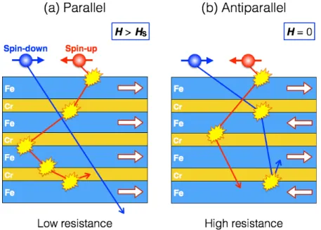
Figure 1.2 Schematic representations of Fe/Cr superlattice structure. (a) The magnetic moments in the Fe layers are parallel when H > HS. (b) The magnetic moments in Fe layers are antiparallel when
H = 0. 4
Figure 1.3 Exchange biased spin-‐valve. (a) Maganetization curve of a layer structure of
FeMn/NiFe/Cu/NiFe, and (b) corresponding MR curve. [12] 5
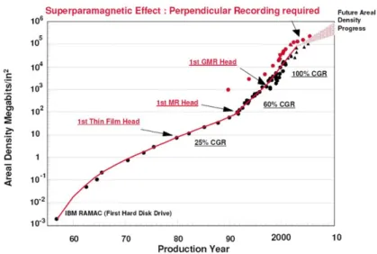
Figure 1.4 Increment of areal density of HDD and contribution of read head. (Hitachi) 5
Figure 1.5 The wave function in a metal-‐oxide-‐metal structure showing schematic concept of quantum-‐
mechanical tunneling for electrons with an energy close to the Fermi energy EF. The barrier
height at the interface between metal and oxide is given by Φ. A nonzero tunneling current is flowing when a bias voltage V is applied between the metallic electrodes. 7
Figure 1.6 Spin-‐resolved tunneling conductivity G for (a) parallel and (b) antiparallel configuration, is
proportional to the product of the DOS factors at the Fermi level EF. The total current in parallel
configuration is governed by Nmaj2EF + Nmin2EF, in the antiparallel case by 2NmajEFNminEF. 8
Figure 1.7 DOS of the elemental metals (a) fcc Cu, (b) fcc Ni, and (c) hcp Co, obtained from self-‐consistent
band-‐structure calculations using the Augmented Spherical Wave (ASW) method. [22] 10
Figure 1.8 Band dispersion of (a) bcc Fe, and (b) bcc Co in the [001] (Γ−H) direction. Thin black and grey
lines represent majority-‐ and minority-‐spin bands, respectively. Thick black and grey lines represent majority-‐ and minority-‐spin bands, respectively. [29] 11
Figure 1.9 The atomic-‐like orbital regrouped by symmetry properties. Δ1, Δ5, Δ2, and Δ2’ are four Bloch
states of different symmetry present around the Fermi level for k ∥= 0. 13
Figure 1.10 Increment of TMR ratio. i-‐ and p-‐MTJ : MTJ with in-‐plane and perpendicular magnetization,
respectively.[36] 14
Figure 1.11 Crystal structure showing easy and hard magnetization directions and respective
magnetization curves for (a) bcc Fe, (b) fcc Ni, and (c) hcp Co. [41] 16
Figure 1.12 Magnetization curves for a ferromagnetic material having a simple cubic symmetry (a) along
the [100], [001], and [101] axes, for a spherical sample. (b) along the [100] and [001] axes, for
plate-‐shaped sample. 17
Figure 1.13 Hysteresis loop with H perpendicular (⊥) and parallel (∥) to the film plane, for Au/Co/Au sandwiches with t = 5.4, 9.5, and 15.4 Å, at T = 10 K. [46] 19
Figure 1.14 Theoretical thickness dependence of (a) the strain and (b) the MAE times the layer thickness
in the coherent and incoherent regime. 21
Figure 1.15 Majority-‐spin (dashed) and minority-‐spin (solid) band structure of Co monolayer along the high-‐symmetry lines of the two-‐dimensional Brillouin zone in the energy range of the d bands. The Fermi energy is denoted by the horizontal line. The predominant character of the minority-‐ spin eigenstates at the high-‐symmetry points is indicated. [59] 30
Figure 1.16 Majority-‐ (dashed) and minority-‐spin (solid) orbital projected d density of states with ml = 0
(top), |ml| = 1 (middle), and |ml| = 2 (bottom), corresponding to the band structure shown in
Figure 1.15. The Fermi energy corresponding to an occupancy of nine electrons is indicated by
the vertical lines. 31
Figure 1.17 Band structure of Co monolayer along high-‐symmetry lines of the two-‐dimensional Brillouin zone, where SOC has been included. Solid curve, magnetization parallel to z; dashed curve, parallel to x. M1 and M2 are the M points along the reciprocal lattice vectors G1 and G2,
respectively, where G2||x. [59] 31
Figure 1.18 Top three panels: anisotropy energy contributed by Γ, Κ, and Μ1 (solid curve) Μ2 (dashed
curve), as a function of the energy corresponding to variable band filling of the fixed band structure. The arrows indicate the position of the energy levels; a double arrow is used to denote doubly degenerate eigenstates. Upward (downward) pointing arrows denote minority-‐ (majority-‐) spin eigenstates. The actual Fermi energy is indicated by the vertical lines.[59] 32
Figure 1.19 Band structure of the Co(2 MLs)/Ni(4 MLs) superlattice for magnetization (a) parallel and (b)
perpendicular to the interfaces. The circles and squares show the most important degeneracy
lifting induced by spin-‐orbit coupling.[61] 34
Figure 1.20 ml-‐resolved density of states for a Co atom of (a) the superlattice Co(1 ML)/Ni(2 MLs), (b)
iv
Figure 1.21 Majority spin (lower panel) and minority spin (upper panel) band structure of the
superlattices (a) Co(1 ML)/Ni(2 MLs), (b) Co(2 MLs)/Ni(1 ML).[60] 37
Figure 1.22 Areal density trends in HDD magnetic recording. [Fujitsu] 38
Figure 2.1 AFM images for the bare MgO (100) substrate. 43
Figure 2.2 Schematic illustrations of microfabrication techniques. 44
Figure 2.3 Snapshot image of MTJ pillar and its electrodes. 45
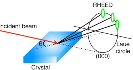
Figure 2.4 A schematic diagram of reflection high-‐energy electron diffraction from a bulk crystal surface.
The incidence angle θ is usually constrained within a few degrees in order to limit the
penetration depth of the electrons into the bulk. 46
Figure 2.5 RHEED patterns from a MgO (100) substrate. a) along the [100] and b) [010] azimuthal
directions, respectively. 46
Figure 2.6 A schematic illustration of vibrating sample magnetometer. 47
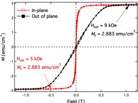
Figure 2.7 Magnetization curves for the standard Ni plate when external magnetic field is parallel (red
curve) and perpendicular (black) to the sample plane. 48
Figure 2.8 (a) a schematic illustration of the MPMS probe and magnet, (b) the configuration of the
second-‐order gradiometer superconducting detection coil. [QuantumDesign] 49
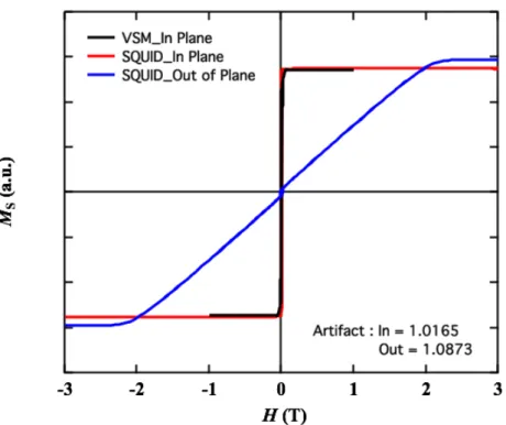
Figure 2.9 The moment artifact of RF-‐SQUID measurement for a Fe thinfilm (dimension : ~ 4 × 4 mm2). 50
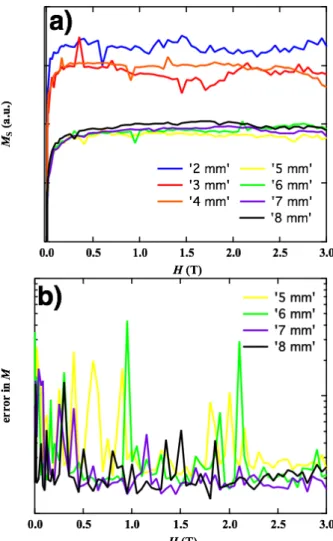
Figure 2.10 (a) Magnetizatoin loops, and (b) error in magnetization values of a Ni standard sample with
respect to vibration amplitude. 51
Figure 2.11 Typical data from CIPT measurement. 52
Figure 2.12 Circuitary for four-‐terminal measurement. 53
Figure 3.1Three different interface configuration. (a) O-‐terminated (pure), (b) over-‐oxidized, and (c) Mg-‐
terminated (under-‐oxidized). 56
Figure 3.2 Spin-‐orbit coupling effect on wave function character at Γ point of interfacial Fe d and O pz
orbitals for O-‐terminated interface. Band levels for out-‐of-‐plane and in-‐plane orientation of magnetization are shown in left and right side of each column. Middle of each column shows the band levels when SOI does not included in calculation. Numbers are the percentage of the orbital character components within Wigner-‐Seitz spheres around interfacial atoms. [10] 57
Figure 3.3 The same as Figure 3.2 for over-‐oxidized Fe/MgO interface. [10] 58
Figure 3.4 RHEED patterns along MgO[100] azimuth. (a) and (b) Cr(001) after annealed at 800°C and
1000°C, respectively. (c) and (d) Fe(001) before annealing. (e) and (f) Fe(001) after annealing at 250°C, when tFe = 0.70 nm. Arrows in (a), (c), and (e) indicate superstructure streaks. 60
Figure 3.5 (a) Bright field TEM image, along [110] direction of Fe layers, of the sample with an adsorbate-‐ induced reconstructed surface after annealing at 400°C. (b) HAADF-‐STEM image taken from a
region surrounded by a solid line in Fig. 2 (a). 61
Figure 3.6 M-‐H loops of the magnetization for Cr (30 nm)/Fe (0.70 nm)/MgO (2 nm) stacks with (a) a clean Fe surface, inset: a magnified M-‐H loop, and (b) an Fe(001) with adsorbate-‐induced
reconstructed surface, after annealing at 400 °C. 62
Figure 3.7 Difference in the value of Keff between the sample with a clean Fe surface (TCr = 1000°C, open
circle) and adsorbate-‐induced reconstructed surface (TCr = 800°C open square) as a function of
Tann. 63
Figure 3.8 Keff of the sample with adsorbate-‐induced reconstructed surface (TCr = 800°C) as a function of
Tann with respect to each thickness of Fe layer, tFe = 0.42 (open circle), 0.70 (open square), and
0.98 nm (open lozenge). 63
Figure 3.9 (a) Electronic transitions in conventional L-‐edge X-‐ray absorption, (b) and (c) X-‐Ray magnetic circular dichroism. The transition occur from the spin-‐orbit split 2p core shell to empty
conduction band states above the Fermi level. In conventional X-‐ray absorption the transition intensity measured as the white line intensity IL3 + IL2 is proportional to the number of d holes N.
By use of circularly polarized X-‐rays the spin moment (b), and orbital moment (c), can be
determined from the dirchroic difference intensities A and B. 65
Figure 3.10 Illustration of the relationship between the bonding states and (a) charge, (b) spin, and (c)
orbital sum rules for the free-‐standing Co monolayer, in anisotropic case. 67
Figure 3.11 Illustration of two different geometries for XMCD measurement. (a) grazing incidence (GI)
and (b) normal incidence (NI) geometries. 70
Figure 3.12 (a) X-‐ray absorption spectra of 0.7-‐nm-‐thick Fe/MgO structures for an annealing
temperature of 450 °C, measured in the NI geometry. (b) XMCD spectra of the NI and GI setups. (c) Integrated XMCD spectra of the NI and GI setups. 71
Figure 3.13 Schematic diagram of the Fe 3d states with the crystal field, surface field, and spin-‐orbit
v
Figure 4.1 Tunneling DOS for k|| = 0 for Fe(100)/Vacuum/Fe(100) calculated using scattering boundary
conditions with Bloch waves incident from the left. The moments of the two iron electrodes are
assumed to be aligned.[11] 81
Figure 4.2 Density of states each atomic layer of Fe(100) near an interface with MgO. (1 hartree equals
27.2 eV)[11] 81
Figure 4.3 Density of states each atomic layer of MgO near an interface with Fe(100).[11] 82
Figure 4.4 A scattering region is connected to the reservoirs through quantum leads. 83
Figure 4.5 Schematic representation of transmission and reflection coefficients and its amplitudes for
Bloch waves from both electrodes. 85
Figure 4.6 Majority conductance for four, eight, and 12 layers of MgO. Units for kx and ky are inverse bohr
radii.[11] 86
Figure 4.7 Minority conductance for four, eight, and 12 layers of MgO.[11] 87
Figure 4.8 Conductance for anti-‐parallel alignment of the moments in the electrodes.[11] 87
Figure 4.9 Tunneling DOS for k|| = 0 for Fe(100)/8MgO/Fe(100). TDOS for (a) majority, (b) minority, (c)
and (d) anti-‐parallel alignment of the moments in the two electrodes.[11] 88
Figure 4.10 (a) The complex band structure of MgO, and (b) Dispersion k2(E) for MgO in the vicinity of the
gap along Δ (100).[11,16] 88
Figure 4.11 Tunneling process through two identical barriers in series separated by a length L. 90
Figure 4.12 (a) Valence-‐band dispersion curves for Ag(111) and Au(111) along the [111] direction. For
each system, a surface state is indicated. The energy window δE for the quantum-‐well states is indicated. (b) Photoemission spectra for, from bottom to top, Au(111), Ag(111) covered by 20 ML of Au, Ag(111), and Au(111) covered by 20 ML of Ag. [18] 91
Figure 4.13 (a) Energy bands in Fe(100) and Cr(100) along the Γ–H symmetry line. (b) s-‐resolved partial
density of states in the eight Fe layers in the QW film of Fe/MgO/FeO/8Fe/Cr at the Γ point. Solid
line, minority spin; Dashed line, majority spin. [19] 93
Figure 4.14 Schematic illustration of the MTJ stacked structure. [25] 95
Figure 4.15 M–H loops for two Cr(30)/Fe(0.7)/MgO(1.8)/Ta(4.5)/Ru(15) (in nm) stacks with annealing
temperatures for Cr layers, TCr, (a) TCr = 800°C (Series-‐I) and (b) TCr = 700°C (Series-‐II). The
whole stacks were post-‐annealed at Tann = 400°C. [25] 95
Figure 4.16 (a) TMR vs. out-‐of-‐plane H curves for the MTJs in Series-‐I and Series-‐II. The inset is the M–H loop for the unpatterned Series-‐I after annealing at 450°C, and (b) TMR ratios as a function of the Tann with respect to each tCoFeB of the two series (Series-‐I : solid lines, Series-‐II: dashed lines).
[25] 96
Figure 4.17 dI/dV curve measured at RT for the MTJ in Series-‐I with tCoFeB = 1.4 nm after annealing at Tann
= 450°C. [25] 97
Figure 5.1 RHEED patterns for (a) mono-‐MgAl2O4 along MgO[100] azimuth, (b) poly-‐MgAl2O4, and (c) a-‐
MgAl2O4 on the Fe(001) layers. [14] 103
Figure 5.2 M−H loops for the Fe (0.7 nm) covered with (a) mono-‐MgAl2O4, (b) poly-‐MgAl2O4, and (c) a-‐
MgAl2O4. [14] 104
Figure 5.3 Annealing temperature dependence of (a) magnetization, (b) Keff, and (c) Ki for the Fe/mono-‐
MgAl2O4, poly-‐MgAl2O4, and a-‐MgAl2O4 structures. [14] 105
Figure 5.4 Schematic illustration of the Fe/Al2O3 bilayer. 107
Figure 5.5 RHEED patterns along MgO[100] and [110] azimuth. (a) Cr (b) Fe(001) (c) Al (d) Al layer after plasma oxidation (e) Al2O3(001) after annealing at 300°C for 30 min. 109
Figure 5.6 M-‐H loops of the magnetization for Cr (30 nm)/Fe (0.70 nm)/Al2O3 stacks after annealing at (a)
300°C, and (b) 450 °C. 109
Figure 5.7 Schematic illustration of the Fe/C60 bilayer. 111
Figure 5.8 Annealing temperature dependence of the magnetic anisotropy characteristic. 112
Figure 5.9 The schematic representation of the set-‐up for the depth-‐resolved XAS and XMCD
measurements. 113
Figure 5.10 Depth-‐resolved X-‐ray absorption, XMCD, and Integrated XMCD spectra for 0.7-‐nm-‐thick Fe/C60 (1ML) structures, measured for the interface and bulk contributions. 114
Figure 5.11 C K edger and Fe L edge (inset) XAS and XMCD spectra of the Fe(001)/C60 (1 ML) structure.
114
Figure 5.12 XAS spectra for C K-‐edge as a function of the photon incidence angle, α, (a) Fe(001)/C60 (3
ML), (b) Fe(001)/C60 (1 ML). (c) partial density of state of C60 at the interface and in the bulk
1
Chapter 1. Introduction – Spintronics
In 1921, German physicists Otto Stern and Walther Gerlach conducted one of the most brilliant experiments in the history of modern physics,1 which is known as the Stern-Gerlach experiment. They
showed that particles (electrons from Ag atoms) possess an intrinsic angular momentum that is quite similar to the angular momentum of a classically spinning object, but that can take only certain quantized values. This intrinsic angular momentum of electrons is now known as “spin”. Particles like electrons have spin as one of the degrees of freedom, which is characterized by a quantum number equal to ± 1 2 with two possible states called “spin-up” and “spin-down”.
Electrons with spin can possess a magnetic dipole moment, which can be experimentally observed in several ways, e.g. the Stern-Gerlach experiment. Although each electron produces the magnetic field, in materials with paired valence electrons, the total magnetic dipole moment of the electron is vanished because the dipole moments from each spin-up and spin-down cancel each other. Therefore, only atoms with unpaired valence electrons can create a macroscopically measureable magnetic field if the dipole moments are aligned parallel to one another. Since in some materials the magnetic dipoles point in random directions in the absence of an external field, i.e. no net magnetic dipole moment, it requires an external magnetic field to align these magnetic dipole moments in the same direction. This phenomenon is called paramagnetism. However, especially in some specific materials, the magnetic dipole moments point in the same direction even in the absence of an external magnetic field (the spontaneous magnetization). This phenomenon is known as ferromagnetism.
A manipulation of electron’s spin for technological applications is termed “spintronics”. Since the spin of electrons can have only the two possible states, this quantum phenomenon may be easily applied to the binary computer systems. In fact, it is considered to be an alternative technology to the conventional “electronics”, because the spin of electrons can remain in its states for long period time. Since the discovery of the giant magnetoresistance (GMR) effect in the late 1980s,2,3 abundant applications such as the magnetic sensor for hard disk drive (HDD) read head, spin-torque oscillator (STO) for microwave generation, spin transistors based on spin injection into semiconductors, and logic devices using a magnetic domain wall etc., are examined and show the possibility to combine those magnetic elements with the conventional electronics devices. In this section, a general aspect of the spintronics will be described through the basic physics and application point of views.
2
1.1.
Magnetoresistance
1.1.1. Giant magnetoresistance (GMR)
Magnetoresistance (MR) is defined as the change in electrical resistance, R, of a material with applied magnetic field (H), which occurs in all metals. The MR (Δρ/ρ) is, where ρ is the resistivity, usually defined by
∆𝜌
𝜌 =
𝑅 𝑯 − 𝑅 0
𝑅 0 (1.1)
,where R(H) and R(0) is the electrical resistance when a finite external magnetic field and no field is applied, respectively. Since the electrical resistance of a material can be manipulated by applying H, the MR is the one of most important properties from the application point of view. Actually, the change in electrical resistance of a material generally depends on the strength of the magnetic field as well as the direction of the magnetic field with respect to current. Although, there are four distinct types of MR: ordinary magnetoresistance (OMR), giant magnetoresistance (GMR), colossal magnetoresistance (CMR), and tunnel magnetoresistance (TMR), the GMR and TMR are actively being studied due to its applicability to the read head for hard disk drive and magnetoresistive random-access memory (MRAM), respectively. Detailed descriptions of GMR and TMR are given in the reminder of this section.
GMR effect is a quantum mechanical MR effect observed in multilayer structures composed of alternating FM and nonmagnetic (NM) layers, which is based on the dependence of electron scattering on the spin orientation, i.e. spin dependent transport. The initial idea of spin dependent transport trace back to Sir Neville Mott’s work in the 1930s4,5; in these papers he developed the two-current model of conduction, and implied that there is a direct connection between the magnetic properties and the electrical conductivity, in the 3d transition FM metals. Among the several factors, two crucial characteristics are mainly responsible for the spin dependent scattering in metallic ferromagnets.
1 In 3d transition metal FMs have a relatively high resistivity compared with noble metals, due to the unoccupied states in the partially filled d bands. And,
2 The exchange interaction leads to unbalanced density of states (DOS) between two spin states (up and down), i.e., the spin polarization, which are responsible for the finite magnetic moment µ, resulting in a different scattering probability and conductivities for spin-up and spin-down electrons.
For T << TC, the 3d transition ferromagnets, such as Fe, Co, and Ni, having those characteristics, can be
well approximated by the two-current model in which the spin-up and spin-down electron currents are considered independently. This has been particularly successful in describing the properties of alloys in which a small quantity of one transition metal (the impurity) is dissolved in another transition metal (the host). The scattering due to certain transition metal impurities is strongly spin-dependent.6 This is due to the combined effects of the spin-splitting of the host d band, the spin-splitting of the impurity d levels and the different hybridization between the host and impurity states for the spin-up and spin-down directions. For example, Cr impurities in Fe scatter the spin-up electrons much more strongly, resulting in a ratio of the
3
resistivities for each spin-state of 𝜌↑ 𝜌↓~6, 𝜌↑ and 𝜌↓ are the resistivities of spin-up and spin-down electrons,
respectively, which implies that if the magnetic moment of impurities is antiparallel to the host magnetization, the resistivity is higher than when they are parallel. However, in these alloy systems, there was no way to control the magnetization of impurities to be parallel or antiparallel with respect to the magnetization of host metal, other than changing the impurities in the alloys. The solution for this problem was the fabrication of antiferromagnetically aligned magnetic layers sandwiched between non-magnetic metallic spacers. The essential for discovery of the GMR effect is interlayer exchange coupling (IEC), which makes able to alter the electrical transport properties of metallic multilayer by applying an external H. The phenomenon has been demonstrated in the systems that contain two FM layers separated by a non-magnetic (NM) layer.7–9 It is found that magnets can interact from long distance through NM spacer to form either
ferromagnetic or antiferromagnetic exchange coupling. Further research leads to the discovery of the GMR effect with using these systems.2,3 A typical MR of Fe/Cr superlattices as a function of external magnetic field is given in Figure 1.1(a), 2 which obtained from Fe/Cr multilayer structure (Figure 1.1(b)).
The type of magnetic coupling in a sandwich structure can directly influence the observed magnetotransport behavior since this is very sensitive to the configurations of magnetizations between the magnetic layers, with the GMR effects being largest for antiferromagnetic coupling. Assume that the magnetization configuration between two Fe layers is antiparallel in zero applied field in an Fe/Cr/Fe structure, and 𝜌↓ << 𝜌↑ (for example, Cr impurities in Fe system : 𝜌↑ 𝜌↓~6)6. Under these assumptions,
there are two cases to consider:
Figure 1.1 GMR effect in Fe/Cr/Fe multilayers, [2] and (b) stacking structure of Fe/Cr/Fe multilayer, arrows represent a magnetization direction.
1. When H > HS (where HS is the saturation field), then the magnetic moments in the Fe layers are parallel
4
1 𝜌= 1 𝜌↑+ 1 𝜌↓ ⇒ 𝜌 ~ 𝜌↓ (1.2) There is an effective short circuit by the less scattered electrons.2. When H = 0, the magnetic moments of the two Fe layers are antiparallel, as Figure 1.2(b). In this case the electrons are alternatively spin-up and spin-down in each of layers with respect to the local magnetization, and the spin-up and –down channels are effectively ‘mixed’, so that 𝜌↓ → 𝜌!", and 𝜌↑ → 𝜌!" where 𝜌!"= 𝜌↑+ 𝜌↓ /2 so that the total resistivity ρ is given by
𝜌 =𝜌↑+ 𝜌↓
4 ≫ 𝜌↓ (1.3)
However, from the application point of view, the GMR effect in multilayer systems have a practical problem to be used for a magnetic sensor, e.g. the read-head of the HDD, that a large external magnetic field is needed to decouple the antiferromagnetic coupling, while it has to sense a small magnetic flux from tiny recording bits. Fortunately, the prerequisite for obtaining GMR effect is not the presence of IEC, but an antiparallel magnetization configuration between two FM layers. By using an antiferromagnet (AF) as a pinning layer, soft magnetic layers made of permalloy, and a dusting of Co at the interfaces between the magnetic layers and NM spacer, Dieny et al. engineered a magnetoresistive sensor, which is called a spin-valve. The magnetization of the on FM layer (pinned layer) is fixed in one direction by the exchange magnetic anisotropy of the adjacent AF layer (pinning layer). The NM spacer layer is sufficiently thick to weaken the coupling so that the magnetization of the other FM layer (free layer) can follow the external field freely. Using the spin-valve composed of FeMn/NiFe/Cu/NiFe, they obtained the GMR output at ~ 10 Oe external fields, which is much smaller than that for the coupled FM/NM systems.10–13
Figure 1.2 Schematic representations of Fe/Cr superlattice structure. (a) The magnetic moments in the Fe layers are parallel when H > HS. (b) The magnetic moments in Fe layers are antiparallel when H = 0.
5
Figure 1.3 Exchange biased spin-valve. (a) Maganetization curve of a layer structure of FeMn/NiFe/Cu/NiFe, and (b) corresponding MR curve. [12]
The magnetization and MR curves of this spin-valve are shown in Figure 1.3.12 These sensors found themselves in commercially available computers, i.e. read head for HDD. IBM commercialized the read head using GMR effect for a recording density of 3 Gb/in2.14,15 As shown in Figure 1.4, the application of GMR read head for HDD contributed to sustain the large increment of the magnetic recording density of HDD. As mentioned above, GMR became the supreme manifestation of spin-dependent transport, and was recognized by the award of the Nobel Prize 2007 to A. Fert and P. Grünberg. Sufficiently large GMR effect were found in FM/NM multilayer structures containing just two to three atomic layers thick because GMR arises largely from spin-dependent scattering, not within the interior of the magnetic layers, but rather from the interfaces between the individual layers, viz. interface scattering.16
Figure 1.4 Increment of areal density of HDD and contribution of read head. (Hitachi)
1298 B.DIENY et al. RT H in plane )) EA 0 CO 2.5 RT H in piane II 0 1.5 CL
~
1. O-C] 0.5 Q ~+soogIIIIy+eeIIOIso++~IOss l -200 0 H (oe) ~ ~ ~ 10 '+++oootej)411IOIgoeg I 200FIG.1. Magnetization curve (a) and relative change in resis-tance (b) for Si/(150-A NiFe)/(26-A Cu)/(150-A NiFe)/ (100-A FeMn)/(20-A Ag). The field is applied parallel to the exchange anisotropy field created by FeMn (EA). The current isAowing perpendicular tothis direction.
variation of magnetoresistance versus the angle (8~
—
82) between the two magnetizations, see inset of Fig. 2. In this structure the NiFe/FeMn bilayer is exchange biased to 170 Oe, with its moment remaining nearly fixed indirection for fields up to
=15
Oe, while the uncoupled NiFe layer can be saturated in any direction in the plane with fields larger than 7 Oe. Thus, by applying a 10Oe rotating field one can rotate the magnetization ofthe soft layer without moving significantly the magnetization ofthe exchange-biased layer. Since 82 is nearly constant, to a good approximation cos(8i
—
8'z) is just the normalized0 2 BOA CU 0.1 0.0 —O.l —0.
2—
2 / I/ 0/0 1component ofthe magnetization ofthe soft layer along the exchange anisotropy field
H,„(see
inset Fig.2).
Two con-tributions are expected for the angular dependence ofthe magnetoresistance. The first one is the usual AMR, which is well-known to vary as the square ofthe cosine ofthe angle between the magnetization and the current. The second contribution is the spin-valve effect. We have directly measured the AMR on the same sample by com-paring resistances for current applied parallel and perpen-dicular to the magnetizations. For both orientations we have used a field sufficiently high tosaturate the magneti-zations of the two NiFe layers. The AMR for only one layer was deduced using the relative thickness ofthe two layers. As shown in Fig. 2, we have subtracted this AMR contribution to single out the angular dependence of the spin-valve eA'ect. Within our error bars, the angular dependence ofthe spin-valve effect is very well represent-ed by a cos(8i
—
82) law. Quantitatively, the amplitude of the spin-valve effect is 3.05% compared to0.
37+
0.02% for the AMR ofthis structure. The latter value is smaller than for bulk NiFe partly due to shunting by the magneti-cally constrained Cu/NiFe/FeMn/Ag component of the structure and partly due tothe increased resistivity ofvery thin NiFe layers. 'We describe next the influence of the interlayer thick-ness on the magnetic and transport properties of films with structure Si/(50-A. NiFe)/(x Cu)/(30-A NiFe)/
(60-A FeMn)/(20-A Ag), with
x
=10,
20, and 26 A. The field is applied parallel to the exchange anisotropy field, the current is flowing perpendicular to this direction. As shown in Fig.3(a)
for x=10
A the two NiFe layers are20A O.l 0.
0—
—0.1 —0.2 — 3 2 0/0 0.2— 0.1—
0.0—
26A cu r~-0.
5 0 i l f f 1 l —1.0 0 0.5 1.0lYli
x:
cos(8i Ge)FIG. 2. Relative change in resistance vs the cosine ofthe rel-ative angle betvreen the magnetizations ofthe toro NiFe layers
of Si/(60-4 NiFe)/(26-A Cu)/(30-4 NiFe)/(60-A FeMn)/ (20-A Ag). Inset shows the orientation of the current
J,
ex-change field H,„,applied field H, and magnetizations Ml and Mp. —0.1 -0.2,~ -0.3—
—0.4 '--100 (c) 2 l —0 0 +100 H (Oe)FIG. 3. Evolution of magnetization (dashed) and magne-toresistance (solid) curves for Si/(50-A NiFe)/(x Cu)/(30-A NiFe)/(60-A FeMn)/(20-A Ag) with Cu layer thickness x
=10,
20, and 26 A. In (c),only the soft film reverses its magnetiza-tion direcmagnetiza-tion in the field range+
100Oe.! 5!
Fig. 1-3 Increment of areal density of HDD and contribution of read head for its increment. GMR read head has contributed that late 90’s (Hitachi).
The GMR read head was already replaced by the tunnel magnetoresistance (TMR) read head with MgO tunnel barrier6, which shows much larger MR output than GMR.
However, in recent years, the TMR read head is thought that the limitation of its usage would come soon as the increment of the recording density of HDD due to the limitation of the signal-to-noise ratio (SNR) because of its large device resistance1. And also, the technological
limit for a fabrication of ultra thin MgO barrier is now facing7. Then, CPP-GMR has been
attracting a big attention as a potential read head application in recent years 8,9,1. Because it is
thought that the SNR for CPP-GMR read head can be better due to its low device resistance.
1.3 Applications of GMR
1.3.1 GMR read head for HDD
There are always demands from the application point of view behind the great development of technologies. As described in last section, the development of GMR has strongly connected the improvement of the magnetic recording density of HDD. Recently, new ways of GMR usage have been proposed and developed. In this section, I described applications of GMR.
6
In the past two decades since the discovery of GMR effect and oscillatory IEC in transition metal systems, the magnitude of the GMR signal exhibited by spin-valve structures has changed very little. The resistance of such structure was typically about 10-15% higher when the magnetization configuration of two FM layers are antiparallel (AP) as compared to that when they are parallel (P). Thus, the interest has been renewed in the past decade in devices based not on dependent diffusive scattering but rather on spin-dependent tunneling through an ultrathin insulating layer forming a tunnel barrier.
1.1.2. Tunnel magnetoresistance (TMR)
In 1975, Jullière observed the tunnel magnetoresistance (TMR) effect in Fe/Ge/Co trilayer structure at low temperature.17 Such multilayer geometry is now known as magnetic tunnel junctions (MTJ). The resistance of a MTJ, which consists of a thin insulating layer (a tunnel barrier) sandwiched between two FM layers (electrodes), depends on the relative magnetization configuration (P or AP) of the electrodes. When a bias voltage is applied across the barrier, finite current flows through the junction because of quantum-mechanical tunneling. The tunneling current through a potential barrier can be described as the finite probability for an electron to tunnel through energetically forbidden barriers. Within the Wentzel-Kramers-Brillouin (WKB) approximation, which is valid for potential U varying slowly on the scale of the electron wavelength, the transmission probability (T) across a potential barrier is in one dimension proportional to:
𝑇(𝐸) ≈ exp −2 ! 2𝑚! 𝑈 𝑥 − 𝐸 /ℏ!d𝑥 !
(1.4)
with E the electron energy, 𝑚! the electron mass, and x the direction perpendicular to the barrier plane. This
equation directly shows the well-known exponential dependence of tunnel transmission on the thickness t and energy barrier U(x) – E, where the electron momentum in the plane of the layers is assumed to be absent, i.e., 𝑘∥= 0. In fact, when electrons are impinging the barrier under an off-normal angle (𝑘∥≠ 0), the
tunneling probability rapidly decreases with increasing 𝑘∥ since in that case the term 2𝑚! 𝑈 𝑥 − 𝐸 /ℏ! in
the exponent of the transmission should be replaced by 2𝑚! 𝑈 𝑥 − 𝐸 /ℏ!+ 𝑘∥!.
In an experimental situation, this tunneling process can be measured in metal-oxide-metal structure, a trilayered structure of two metal electrodes separated by a thin insulating layer. The metal-oxide-metal junction is drawn in Figure 1.5 where the potential of the barrier U(x) is assumed to be constant across the barrier and located at an energy Φ above the Fermi energy EF of the metal layers. Without a voltage
difference between the metal layers, the Fermi levels will be equal on either side of the barrier, and the tunnel current is zero. When a finite bias voltage V is applied, the Fermi level is lowered at the right-hand side of the barrier, and electrons are now able to elastically tunnel from filled electron state (left) towards unoccupied states in the second (right) electrode. (Note that in this case the electrode at right is at a higher electrical potential as compared to the left electrode, yielding a net electrical current from right to left.).
7
Figure 1.5 The wave function in a metal-oxide-metal structure showing schematic concept of quantum-mechanical tunneling for electrons with an energy close to the Fermi energy EF. The barrier height at the
interface between metal and oxide is given by Φ. A nonzero tunneling current is flowing when a bias voltage V is applied between the metallic electrodes.
As a result, the amount of current will be proportional to the product of the available, occupied electron states on the left, and the number of empty states at the right electrode, multiplied by the barrier transmission probability. Therefore, the tunneling current is directly proportional to the density-of-states (DOS) of each electrode (at a specific energy E) multiplied by the Fermi-Dirac factors f(E) and 1 – f(E) to account for the amount of occupied and unoccupied electron states, respectively.
The net tunneling current in the metal-oxide-metal structure can be calculated by considering the current due to electrons tunneling from left to right assuming an elastic (energy-conserving) electron tunneling process from occupied states on the left to empty states at the right (see Figure 1.5)
𝐼!→!(𝐸) ∝ 𝑁! 𝐸 − 𝑒𝑉 𝑓 𝐸 − 𝑒𝑉 𝑇 𝐸, 𝑉, 𝜙, 𝑡 𝑁! 𝐸 1 − 𝑓 𝐸 (1.5)
As indicated by Eq. (1.4), the transmission T(E,V, 𝜙,t) depends on the electron energy and barrier thickness and potential, but it is also affected by the bias voltage V that effectively reduces the barrier height 𝜙. The similar equation for the opposite current can be easily deduced, then the total current I is obtained by integrating 𝐼!→!− 𝐼!→! over all energies:
𝐼 ∝ !!𝑁! 𝐸 − 𝑒𝑉 𝑇 𝐸, 𝑉, 𝜙, 𝑡 𝑁! 𝐸 𝑓 𝐸 − 𝑒𝑉 − 𝑓 𝐸 d𝐸
!!
(1.6)
For small voltage eV << 𝜙 only the electrons at (or close to) the Fermi level EF contribute to the tunneling
current, by which the transmission no longer depends on energy E. Moreover, in this limit also the DOS factors are in principle independent of E, which reduces the current to:
𝐼 ∝ 𝑁! 𝐸! 𝑁! 𝐸! 𝑇 𝜙, 𝑡 𝑓 𝐸 − 𝑒𝑉 − 𝑓 𝐸 d𝐸 !!
!!
8
Figure 1.6 Spin-resolved tunneling conductivity G for (a) parallel and (b) antiparallel configuration, is proportional to the product of the DOS factors at the Fermi level EF. The total current in parallel
configuration is governed by 𝑁!"#! 𝐸
! + 𝑁!"#! 𝐸! , in the antiparallel case by 2𝑁!"# 𝐸! 𝑁!"# 𝐸! .
Furthermore, at low enough temperature (kBT << eV), the integral over the Fermi functions simply yields eV,
thus the transparent expression for the tunnel conductance can be deduced as follow:
𝐺 ≡ d𝐼/d𝑉 ∝ 𝑁! 𝐸! 𝑁! 𝐸! 𝑇 𝜙, 𝑡 (1.8)
In this simple model, it shows that the tunnel conductance is proportional to the transmission probability and the DOS of the two electron systems. Based on the tunnel conductance in the metal-oxide-metal structure, the tunneling current in MTJ can be evaluated as depicted in Figure 1.6. The DOS of a FM is represented by simple majority and minority electron bands, which are shifted in energy due to exchange interactions. Here, MTJ with two identical FM electrodes separated by an insulating barrier is considered. When magnetization orientation of two FM electrodes are parallel to each other, tunneling may only occur between bands of the same spin orientation in either electrode, i.e. from a spin majority band to a spin majority band, and similar for the minorities. (With an assumption that the electron spin is conserved in these processes18) Using Eq. (1.8) and assuming equal transmission for both spin species, the conductance for parallel configuration can be written as:
𝐺!= 𝐺↑+ 𝐺↓∝ 𝑁!"#! 𝐸
! + 𝑁!"#! 𝐸! (1.9)
where 𝐺↑(↓) is the conductance in the up- (down-) spin channel, and 𝑁!"# 𝐸! (𝑁!"# 𝐸! ) is the majority (minority) DOS at EF. When the magnetization direction of one FM electrode is changed relative to that of
9
Tunneling under such spin orientation now means tunneling from a majority to a minority band, and vice versa. The conductance for antiparallel configuration is then simply:
𝐺!"= 𝐺↑+ 𝐺↓∝ 2𝑁!"# 𝐸! 𝑁!"# 𝐸! (1.10)
It is immediately clear that conductances are different for parallel and antiparallel configuration. In other words, FM tunneling junctions display a MR when an external field is used to switch between these magnetic orientations. This TMR is usually defined as the difference in conductance between parallel and antiparallel configuration, normalized by the antiparallel conductance, or, alternatively, as the resistance change normalized by the parallel resistance:
TMR ≡𝐺!− 𝐺!" 𝐺!" =
𝑅!"− 𝑅!
𝑅! (1.11)
Note that the equality of the two definitions for TMR is only valid for very small bias voltage, since in that case the inverse tunnel resistance R-1 = I/V is identical to the conductance dI/dV. Using Eq. (1.9) and (1.10), it is easily derived that TMR is equal to 𝑁!"# 𝐸! − 𝑁!"# 𝐸! !/ 2𝑁!"# 𝐸! 𝑁!"# 𝐸! . Generalizing this for two different magnetic electrodes results in the well-known Julliere-formula for the magnetoresistance of MTJ’s17:
TMR = 2𝑃!𝑃!
1 − 𝑃!𝑃! (1.12)
where 𝑃!(!) is the tunneling spin polarization in the left (right) FM electrode. The tunneling spin polarization
of each electrode is defined as
𝑃 = 𝑁!"# 𝐸! − 𝑁!"# 𝐸!
𝑁!"# 𝐸! + 𝑁!"# 𝐸! (1.13)
and is simply the normalized difference in majority and minority DOS at the Fermi level. From these equations it is immediately seen that in the limit of zero polarization of one of the electrodes, no TMR is expected. On the other hand, for a full polarization of ±1, the TMR becomes infinitely high.
Although the basic physics of tunneling conductance in MTJ structure can be understood by considering the elementary approach above, it fails to predict a number of experimental observations. These observations for TMR include, for instance:
1 strong dependence of TMR on the applied bias voltage V and temperature T
2 sensitivity of TMR on the electronic structure of the barrier-ferromagnetic interface region, not just the bulk DOS (as suggested by Eqs. (1.12) and (1.13))
3 relevance of the electronic structure of the barrier, in some cases even leading to an inversion of TMR. In order to appreciate these observations, the better understanding about the role of tunneling spin polarization in the physics of MTJ is needed. The tunneling spin polarization of individual magnetic electrodes can be measured with a superconducting tunneling spectroscopy (STS) technique that uses a superconductor (in most cases Aluminium) to probe the spin imbalance in tunneling currents. According to the STS results, it has been known that the tunneling spin polarization of the 3d ferromagnetic metals are all positive, and in the range of 40-60%.19,20 As expressed in Eq. (1.13), the positive sign of the polarization
10
relates to a dominant majority DOS at the Fermi level. However, calculated DOS for Co and Ni shows completely reversed situation,21 having surplus of minority states of the Fermi level, as shown in Figure 1.7.
This would suggest a negative tunneling spin polarization, and completely contradicts the experimental observations. Theoretically, it has shown that the conductance in a tunnel junction is not simply determined by the electron DOS at the Fermi level, but should include the probability for them to tunnel across an ultrathin barrier.22 Especially, the most mobile s-like electron states are able to tunnel with a much larger
probability as compared to the d electrons due to their different effective mass, 𝑚!∗ ≫ 𝑚!∗~𝑚!. Based on this,
the positive spin polarization can be explained by considering the spin asymmetry of the s-like energy bands, thereby neglecting the contribution from the rapidly decaying d-like wave functions in tunneling experiments.
Moreover, it has been calculated by Slonczewski that spin-dependent tunneling is not a process solely related to the (complex) electronic properties of the FM electrodes.23 He has analytically calculated the
tunneling current between free-electron FM metals within the WKB approximation, assuming that tunneling electrons have a very small parallel wave vector. By explicitly matching the electron wave functions at the barrier interfaces, the tunneling spin polarization is calculated as:
𝑃 = 𝑃!×
𝜅!− 𝑘
!,!"#𝑘!,!"#
𝜅!+ 𝑘
!,!"#𝑘!,!"# (1.14)
where 𝑘!,!"# and 𝑘!,!!" are the Fermi wave vectors, and κ is the imaginary component of the wave vector
of electrons in the barrier with 𝑘∥= 0 at the Fermi level, corresponding to 𝜅 = 2𝑚!𝜙/ℏ! !/! with 𝜙 the
height of the barrier. The first term P0 is equal to the Eq. (1.13). The second term, however, contains the
properties of the barrier as well, and is due to the discontinuous change of the potential at the interface with the barrier. As a result of this interface factor, the polarization becomes greatly dependent on the band paraeters in relation to the height of the barrier, with the possibility to even change the sign of P. This is in fact a first demonstration that tunneling spin polarization is not an intrinsic property solely determined by the FM electrode. This free-electrons formalism has been successfully used to describe the magneto-transport properties in polycrystalline MTJ (typically involving amorphous aluminium oxide barriers).24 By
fitting the experimental transport characteristics with analytical free-electrons models one can extract parameters such as the barrier width and height for a given experimental system.
Figure 1.7 DOS of the elemental metals (a) fcc Cu, (b) fcc Ni, and (c) hcp Co, obtained from self-consistent band-structure calculations using the Augmented Spherical Wave (ASW) method. [22]
Spin-Dependent Tunneling in Magnetic Junctions 11
1.3 Beyond the elementary approach
Although the model we have introduced captures some of the basic physics in
mag-netic tunnel junctions and is rather illustrative on a tutorial level, it fails to predict
a number of experimental observations. These observations for TMR include, for
instance:
• strong dependence of TMR on the applied bias voltage V and temperature T
• sensitivity of TMR on the electronic structure of the barrier-ferromagnetic
inter-face region, not just the bulk density-of-states (as suggested by Eqs.
(9) and (10)
)
• relevance of the electronic structure of the barrier, in some cases even leading to
an inversion of TMR.
Here we will briefly introduce some of the advanced theories to better
appreci-ate these observations, focusing at this point on the tunneling spin polarization for
its fundamental role in the physics of magnetic tunnel junctions. A more detailed
treatment will be postponed for sections
3 and 4
.
Later on in this review (
Table 1.2
in section
3
) we will show that the
tun-neling spin polarization of the 3d ferromagnetic metals are all positive, and in the
range of 40–60%. According to the definition of Eq.
(10)
, the positive sign of the
polarization relates to a dominant majority density-of-states at the Fermi level. If
one considers the band structure and density-of-states of the 3d metals, however,
the situation is completely reversed. As an example,
Fig. 1.6
shows the (calculated)
density-of-states of Co and Ni, both having a surplus of minority states of the
Fermi level. This would suggest a negative tunneling spin polarization, and
com-pletely contradicts the experimental observations. This dichotomy was recognized
already in the seventies when pioneering experiments in the field of
superconduct-ing tunnelsuperconduct-ing spectroscopy were reported on ferromagnetic-superconductsuperconduct-ing
junc-tions (
Tedrow and Meservey, 1971a, 1971b, 1975
). Theoretically,
Stearns (1977)
has
shown that the conductance in a tunnel junction is not simply determined by the
electron density-of-states at the Fermi level, but should include the probability for
them to tunnel across an ultrathin barrier. Especially the most mobile s-like electron
states are able to tunnel with a much larger probability as compared to the d
elec-trons due to their different effective mass. Based on this, Stearns could explain the
positive spin polarization by considering the spin asymmetry of the s-like energy
Figure 1.6 Density-of-states of the elemental metals fcc Cu (a), fcc Ni (b), and hcp Co (c), obtained from self-consistent band-structure calculations using the Augmented Spherical Wave (ASW) method. From Coehoorn (2000).
![Figure 1.1 GMR effect in Fe/Cr/Fe multilayers, [2] and (b) stacking structure of Fe/Cr/Fe multilayer, arrows represent a magnetization direction](https://thumb-ap.123doks.com/thumbv2/123deta/8499278.922993/11.892.142.727.708.1010/figure-multilayers-stacking-structure-multilayer-represent-magnetization-direction.webp)
![Figure 1.12 Magnetization curves for a ferromagnetic material having a simple cubic symmetry (a) along the [100], [001], and [101] axes, for a spherical sample](https://thumb-ap.123doks.com/thumbv2/123deta/8499278.922993/25.892.171.728.105.386/figure-magnetization-curves-ferromagnetic-material-having-symmetry-spherical.webp)