Spin and charge transport properties in
magnetic materials with lowered symmetry
著者
Chen Yao
学位授与機関
Tohoku University
博士論文
Spin and charge transport properties in
magnetic materials with lowered symmetry
(低対称性の磁性体中のスピン・電荷輸送特性)
Chen, Yao
(陳
)
(別紙様式5)
論 文 内 容 要 旨
(NO.1) 氏 名 CHEN, Yao 提出年 令和 2 年 学位論文の 題 目Spin and charge transport properties in magnetic materials with lowered symmetry
(低対称性の磁性体中のスピン・電荷輸送特性)
論 文 目 次
1 Introduction 1
1.1 Spin current ……….…… 2
1.1.1 Electron spin currents and magnon spin currents ……… 2
1.1.2 Spin Hall effect and inverse spin Hall effect ………. 3
1.1.3 Spin-Seebeck effect ……… 5
1.2 Spin and charge in one-dimensional solid state materials ……….. 11
1.2.1 One-dimensional fermion system ……… 11
1.2.2 One-dimensional spin-1/2 system ……… 14
1.2.3 One-dimensional spin-1/2 system with frustration and dimerization ………. 16
1.3 Soliton excitation in one-dimensional spin chain: spinon and triplon ………. 17
1.3.1 Ground state and the soliton excitation in the Heisenberg-δ-α model ……… 17
2 Experimental details 27
2.1 Sample fabrication and evaluation methods ……… 27
2.1.1 Fabrication of CuGeO3 single crystal ……… 27
2.1.2 Magnetron sputtering ……… 31
2.1.3 Electron beam lithography ……… 33
2.2 Measurement methods ……… 34
3 Triplon spin current in CuGeO3 39
3.1 Introduction ……… 39
3.1.1 Spin-Peierls transition ……… 39
3.1.2 CuGeO3 ……… 40
3.2 Properties of the CuGeO3/Pt sample ……… 45
3.3 SSE in CuGeO3/Pt sample ……… 49
(別紙様式5)
(NO.2)
3.5 Boltzmann approach to the triplon SSE ………. 59
3.6 Interfacial SSE approach to the triplon SSE ……… 65
3.7 Discussion and conclusion ………... 70
4 Transport properties of superconducting vortices in 1D magnetic domain structures 71
4.1 Introduction ……… 71
4.1.1 Ginzburg-Landau theory of superconductivity ……… 71
4.1.2 Superconducting vortex ……… 74
4.1.3 Concept of the study ……… 79
4.2 Sample characterization ……… 81
4.2.1 Superconducting properties ……… 81
4.2.2 Magnetization of the Y3Fe5O12 film ……… 84
4.3 Anisotropic transportation of superconducting vortices ……… 84
4.4 Discussion and Conclusion ……… 93
5 Conclusion 95
6 Appendix 97
6.1 Relevant, irrelevant and marginal terms in the Heisenberg-δ-α model ……… 97
6.2 Excitation gap of one-dimensional spin chain ……… 98
6.3 Soliton and anti-soliton solution of the Sine-Gordon equation ……… 99
7 Acknowledgements 102
Publication list 104
Chapter 1
Introduction
The aim of this dissertation is to investigate the transport phenomena of spin and charge excitation in low-symmetry magnetic structures. The first and second parts of this disser-tation investigate the transport of two types of excidisser-tations, triplon and superconducting vortex, in one-dimensional magnetic structures.
In the first part (Chapter 3), we report the discovery of triplon spin current, carried by soliton excitations in the spin-Peierls material CuGeO3 with a one-dimensional spin chain.
Low-dimensional magnets are known to have exotic magnetic orders different from three-dimensional ones due to their three-dimensionality. Spin current transport of spin excitations (spinon) in spin liquids without long-range correlations is reported in 2016[1], but there are still few studies done in terms of spin current in Low-dimensional magnets. In this study, we investigate the spin current transport properties of solitons in spin-Peierls-ordered CuGeO3.
It is found that the spin current is significantly different from the magnon spin current in three-dimensional magnets. This result is expected to extend spintronics to a broader category of dimer-ordered magnets.
The second part (Chapter 4) is a search for the transport phenomena of superconducting vortices in a one-dimensional magnetic domain. Superconducting vortices are topological excitations in second type superconductors and are topologically protected and therefore not dissipated in the sample. The application of spintronics using vortices, which also carry angular momentum, has recently been reported. For example, long-range spin current trans-port is investigated using vortex flow[2]. To regulate the flow of the vortices, the transport of the vortices in one-dimensional magnetic domains is investigated in this dissertation.
In this introductory chapter, I will first review recent developments in spintronics from a fundamental perspective. After that, I will introduce one-dimensional magnets and explain solitons, which are topological excitations in them.
1.1 Spin current 2
1.1 Spin current
Jse Jce
(a) Charge current (b) Electron spin current
Bex m
Jsmagnon
(c) Magnon spin current
Figure 1.1: Schematic illustrations of (a) charge current Je
c, (b) electron spin current Jse, and (c) magnon spin current Jmagnon
s . In a paramagnetic metal, the electron spins are randomly polarized. Therefore, the current has no spin polarization on average. For a pure electron spin current, up-spin and down-spin electrons are moving in opposite directions with the same amount of electrons. The charge current in this case is zero. In magnetic insulators, elementary excitations of local spin momentum (magnons) can also carry pure spin currents. As the name implies, the spin current is a flow of spin angular momentum. The for-mulation of the spin current Js is given by the conservation equation of magnetization M as[3]
1
γ dM
dt + ∇ · Js= T . (1.1)
Where γ and T represent the gyromagnetic ratio and spin relaxation. The spin current, unlike the charge current, is a second-order tensor, whose indices represent the direction of spin flow and the direction of the spin eigenvalue. In the following discussion, the second index will be set to 3 (i.e., the spin measured along the z-axis, with two eigenvalues σ =↑ and σ =↓).
1.1.1 Electron spin currents and magnon spin currents
In metals and semiconductors, spin-polarized electrons carry electron spin currents. Let the creation and annihilation operators of electrons be c†
k,σ and ck,σ. Then the spin along
the z-axis is given by sk= !2(c†k,↑ck,↑− c†k,↓ck,↓) and the electron spin current is[4]
Jse= ! 2 ! vk " %c†k,↑ck,↑& − %c†k,↓ck,↓& # . (1.2)
1.1 Spin current 3 The charge current (the flow of electrons) is
Jce= e! k vk " %c†k,↑ck,↑& + %c†k,↓ck,↓& # . (1.3) If Je
s '= 0 and Jce = 0 are satisfied, then the spin current is called pure spin current (illus-trated in Fig. 1.1(b)). In ferromagnetic metals, the charge current is always accompanied by a spin current (not a pure spin current) because the spin polarization is non-zero.
In magnets, the elementary excitations of localized magnetic momentum (magnons) also carry a pure spin current, which is called the magnon spin current[3, 4]. Similar to the electron spin current, if the magnon creation and annihilation operators are b†
k and bk, then
the magnon spin is given by sk = b†kbk. The creation of the magnon decreases the total
magnetization of the magnet. If we note that the direction of magnetization and the electron spin is opposite, the magnon spin is in the same direction as the magnetic field. The magnon spin current is given by[4]
Jsm= 1 2!
! k
vk%b†kbk& (1.4)
Neither the electron spin current nor the magnon spin current is a conserved current because of the spin relaxation term in Eq. 1.1. Electron spin current lose spin information on a length scale called spin diffusion length, as the electron spins are inverted due to both magnetic impurity scattering and spin-orbit coupling. The spin diffusion length of a metal is typically a few hundred nanometers or less[3]. For magnon spin currents, damping losses and electron-magnon scattering also leads to a diffusion length. However, in low-damping magnetic insulators, the diffusion length can be as long as a few millimeters[5].
1.1.2 Spin Hall effect and inverse spin Hall effect Spin Hall effect
When a bias current is applied to a metal or semiconductor under a magnetic field, a voltage perpendicular to both the bias current and the magnetic field appears in the material. This effect is known as the Hall effect. The transverse voltage is due to the Lorentz force acting on the charge carriers. When a bias current is applied to a ferromagnetic metal in the absence of a magnetic field, a similar transverse voltage appears. This effect is called the anomalous Hall effect (AHE), and its origin is the spin-orbit coupling[3,6]. Due to the spin-orbit coupling, the up-spin and down-spin electrons in the ferromagnet are shifted in opposite directions, as shown in the Fig. 1.2(a). Since there are more up-spins than down-spins, an electron current (which is also a spin current) is generated along the transverse direction.
1.1 Spin current 4
+
-Electron currentJce Spin current Jse (b) SHE+
-Electron currentJceSpin current + electron current
J s e + J ce (a) AHE z x y (c) ISHE Electron currentJce Spin current Jse
V
Figure 1.2: Schematic illustration of (a) Anomalous Hall effect, (b) Spin Hall effect, (c) Inverse spin Hall effect.
The same phenomenon also occurs in paramagnetic metals with strong spin-orbital cou-pling. However, in this case, the number of up and down spins is equal and a pure spin current is induced in the transverse direction. This effect is known as the spin Hall effect (SHE). As shown in Fig. 1.2(b), the input electron current Je
c1 induces a transverse spin current Jα
s as:
Jsα= θSHˆα × Jce. (1.5)
Here, ˆα = ˆx, ˆy, ˆz and θSH is coefficient repersenting the conversion efficiency of the spin
current, called the spin Hall angle.
The SHE was first proposed theoretically by Dyakonov and Perel in 1971[7, 8, 9]. In 2004, Kato et al. used the magneto-optical Kerr effect to directly observe the accumulation of spins at the edge of a semiconductor and experimentally detected the spin Hall effect[10]. A year later, Wunderlich et al. also observed the SHE by directly measuring the polarization of light emitted from two p-n junctions with different spin accumulation due to the SHE[11].
Inverse spin Hall effect
The inverse process of the spin Hall effect is known as the inverse spin Hall effect (ISHE, see Fig. 1.2(c)), which has the same microscopic mechanism as the SHE. Electrons with different spin polarization are scattered in the opposite direction by spin-orbital coupling. The ISHE takes a spin current Jα
s as input and outputs an electron current Jce as follows: Jce= θSH
! α
Jsα× ˆα. (1.6)
1.1 Spin current 5 The ISHE was discovered experimentally by several groups in 2005-2006. Two of them are shown in Fig. 1.3. Valenzuela and Tinkham[12] used the nano-devices as Fig. 1.3(a). They used one ferromagnetic nanowire to inject a spin current into an Al wire and another wire to detect the non-local ISHE signal due to the diffusive spin current. On the other hand, Saitoh et al.[13] used ferromagnetic resonance (FMR) to excite magnons and inject the spin current into the conjunct Pt layer. The ISHE signal was detected as a DC voltage. ISHE is a powerful tool for detecting spin current and is now a widely used technique. Pt has been used as a model material for spin current detection because of its relatively large spin Hall angle[3] and ease of fabrication by the sputtering method.
1.1.3 Spin-Seebeck effect
The spin-Seebeck effect (SSE) is a phenomenon of thermal generation of spin currents in a magnet/heavy metal hybrid under a temperature gradient. The spin current in the magnet propagates along the temperature gradient and is injected into the heavy metal, allowing the spin current to be detected as a voltage signal via the ISHE. The SSE was first reported in 2008 in a Permalloy(Py)/Pt hybrid by Uchida et al.[14] It was performed with the experimental setup shown in Fig.1.4(d) (known as transverse SSE or TSSE). The sample is subjected to an in-plane thermal gradient and an electron spin current is generated across Py. However, other unintended effects occur in this experimental setup[15]. Specifically, the longitudinal SSE and anomalous Nernst effect (ANE) are found to occur due to the induction of a local longitudinal thermal gradient at the metal stripe, depending on the material of the voltage contacts.
On the other hand, the longitudinal SSE (LSSE) setup [16] has become more main-stream in recent years; in the case of LSSE, the thermal gradient is applied perpendicular to the bilayer sample and parallel to the spin current across the interface. Fig. 1.4(f) shows the LSSE signal for a magnetic insulator Y3Fe5O12/Pt sample. By using an insulator as
the magnetic material, parasitic ANE signals in LSSE measurements can be eliminated. This has led to numerous studies of the Y3Fe5O12/Pt system as a model system in the
magnonic spin current system, including high-temperature measurements up to the Tc of Y3Fe5O12[18], the substitution of Y and Fe sites by other elements[19], the thickness
depen-dence of Y3Fe5O12[20, 21, 22, 23], and the relaxation length of magnons in Y3Fe5O12[24].
The possible proximity effect induced ANE in the Pt film (which is pointed out by Qu
et al.[25]) was also ruled out by Kikkawa et al.[26].
Since its discovery in the ferromagnet/Pt system (see [17] as a review), the SSE has also been observed in ferri-[24,27] and antiferromagnetic[28,29,30] materials. The temperature
1.1 Spin current 6
(b)
(a)
Figure 1.3: (a) Detection of ISHE signal in a non-local nano-device[12]. (b) ISHE signal detection under FMR[13]. This setup is also known as the spin pumping.
1.1 Spin current 7
J
sbackJ
s backJ
spump∇T
T
(a) (b)J
spump (c) (d) (e) Conductor Magnets Insulator 100 K 200 K 300 K Temperature 0 K∇
T
∇
metal ferromagnetV
H
H
J
sJ
sJ
sE
ISHEE
ISHEE
ISHE (f) (g)Transverse spin Seebeck effect Longitudinal spin Seebeck effect
z x y
H
effFigure 1.4: (a) Thermal spin pumping: due to thermal fluctuation of the magnetic momen-tum in the ferromagnet layer, spin current is injected into the metal layer. (b) Back flow spin current injected from the metal layer to the ferromagnet layer. (c) The spin Seebeck effect (SSE): net spin current transfer in the bilayer under thermal gradience. (d) Transverse spin Seebeck effect (TSSE). (e) Longitudinal spin Seebeck effect (LSSE) (f) A typical result of longitudinal SSE[16]. (g) SSE in various magnetic materials[17].
1.1 Spin current 8 and magnetic field dependence of SSE in these conventional magnetic orders reflect the trans-port properties of the magnetic excitation (magnon or antiferromagnetic magnon)[31] and the response of dynamical magnetic susceptibility (ImχR) towards external environments[4]. For example, the magnetic field suppression of the SSE in ferromagnet/Pt reveals both a spectrum shift in ImχR due to the Zeeman effect and wave-number dependent magnon scattering during transport in bulk. In recent studies, the SSE is found even in exotic mag-nets with strong quantum and thermal fluctuations that ordinary magnetic order does not appear. The SSE in quantum spin liquids[1], spin-nematic liquids[32], and paramagnetic insulators with dipole interactions[33, 34, 35], for instance, have been reported. The SSE in these exotic magnets gives us information on the transport properties and ImχR of spin excitations just as the magnon SSE. But at the same time, the polarization direction of the dominant spin excitations (i.e. the sign of the ImχR) can also be extracted by comparing the sign of SSE with the magnon case. Using the SSE, we can classify magnetic materials, especially those without conventional magnetic order, according to the polarization direction of the spin excitations.
Dynamical magnon theory for SSE
In 2010, Xiao et al.,[36] provided a theoretical explanation of the SSE. The magnetization of the ferromagnetic layer precesses around the effective field (Heffˆz, as shown in Figs.
1.4(a)-(c)), leading to a spin-pumping spin current as js,pump = ! e $ gr↑↓m×∂m ∂t + g ↑↓ i ∂m ∂t % . (1.7)
The authors consider the Landau–Lifshitz–Gilbert equation in addition with the thermal fluctuation term as ∂m ∂t = −γm × (Heffˆz + h) + α Ms m×∂m ∂t . (1.8)
Here, h is the random thermal effective magnetic field in the ferromagnetic layer. On the other hand, the back flow spin current from metal to ferromagnet is
Js,back = −MsV
γ γm× h
#. (1.9)
Where h# is the random thermal effective magnetic field in the metal. The net spin current
js is given by a combination of the pumping and backflow terms. To model the thermal gradient applied across the interface, different effective temperatures are assumed for the metallic (Te) and ferromagnetic (Tm) layers. The magnetic fields h and h# are assumed
1.1 Spin current 9 approach, they found the net spin current to be
%Js& )
γ!gr↑↓kB
2πMsV (Tm− Te) (1.10)
In the thermal equilibrium, Tm = Te and the net spin current is zero. When Tm '= Te (as shown in Fig. 1.4(c)), the net spin current is no longer zero, and a voltage signal is observed in the metal layer.
Interfacial SSE theory
Adachi et al.[37, 4] proposed a microscopic model of SSE based on the interfacial ex-change interaction (Jsd) between localized spins in the ferromagnet and electron spins in
the metal. This theory relies on physical processes at the interface and does not take into account the spin current transportation process and spin current generated in the bulk, hence it is called as the interfacial spin Seebeck theory. The net spin current across the interface is calculated based on Keldysh Green’s function in a perturbative approach with respect to Jsd as Js∝ Jsd2 ˆ ∞ −∞ dωImχ−+R (ω)ImXR−+(ω)[fB(Tm) − fB(Te)]. (1.11) Here, χ−+
R /XR−+ and fB(T ) are magnetic susceptibility of metal/magnet and Bose
distri-bution function, respectively. The explicit expression of Imχ−+
R in a paramagnetic metal is ω-odd function[1,37] as
Imχ−+
R = 1 + τχ0ωτ2s
sω2, (1.12)
where χ0 and τs are the static susceptibilities and the spin relaxation time. They are both
insensitive to temperature and magnetic field. since the distribution function is also a known function, the temperature and magnetic field dependence is hidden in the term of X−+
R .
Let’s see the expression of X−+ R [1,38]: X−+(ω) = −1 N ! k ˆ β 0 dτexp(iωnτ) N ! j
exp(−ikj) %TτSj−(τ)S0+(0)&iωn→ω+i0+, (1.13)
where N is the number of sites, τ is the imaginary time, β = 1/T , ω = 2πn/β (where n is integer), and Tτ is the imaginary time ordering operator. So, in this theory, the spin current injected into the metal layer is formulated as a correlation function of the localized spins in the magnetic insulator. Since the spin correlation function contains information about many-body effects and material parameters, it is particularly useful for revealing the nature of spin excitations in magnets without conventional magnetic order.
1.1 Spin current 10 The theory is used to explain experimental results of the SSE in ferrimagnet/Pt[20]; compensated ferrimagnet/Pt and antiferromagnet/Pt[39] systems; Tomonaga-Luttinger spin liquid/Pt[1] and spin-nematic/Pt[32] systems.
Boltzmann transport theory for SSE
When the SSE signal is measured as a function of the thickness of the magnetic insula-tor[20,23], the signal increases with increasing thickness and becomes saturated at a certain thickness. The results of the magnetic insulator thickness dependence indicate that the in-terfacial picture[36, 37] alone is not sufficient to explain the SSE mechanism and a theory based on bulk magnon propagation is needed. In other words, we need a physical model of the magnon from its generation to its arrival at the interface. The transport process inside the bulk of the ferromagnet can be described phenomenologically by the Boltzmann equa-tion and the magnon scattering process can be modeled by the relaxaequa-tion time (τk(H, T )) approximation.
A theoretical model of SSE based on thermally driven magnons in magnetic layers is proposed by Rezende et al.[31,40,41]. Their idea is to consider a non-equilibrium magnon distribution nk(x), which is an deviation from the thermal equilibrium (Bose-Einstein dis-tribution n0
k). The non-equilibrium magnon number is given by
δnm(x) = (2π)1 3 ˆ
d3k&nk(x) − n0k '
, (1.14)
and the magnon spin current is Jsz = ! (2π)3 ˆ d3kvk & nk(x) − n0k ' . (1.15)
Here, vkis the velocity of magnon. The steady-state Boltzmann equation and the relaxation approximation gives
nk(x) − n0k = −τkvk· ∇nk(x). (1.16)
By combining this and Eq. 1.15, we can calculate the net magnon spin current Jz s as Jz
s = Jsz∇T + Jsδnz . The first term is proportional to the temperature gradient ∇T and the second term represents the diffuse magnon flow due to the accumulation of magnons.
The model reproduces the temperature and the Y3Fe5O12 thickness dependence[31] of
SSE in Y3Fe5O12/Pt samples. The high field suppression of the SSE signal[21,23] at room
temperature can be explained in the Boltzmann framework by assuming that low-frequency magnons contribute more to the signal than high-frequency magnons since the relaxation time depends on k[40]. The non-local spin transport in Y Fe O is also studied using this
1.2 Spin and charge in one-dimensional solid state materials 11 approach[42]. The Boltzmann approach to SSE is also applied to other types of magnets[43, 41,44], and we will use it to formalize the triplon spin current in the following sections.
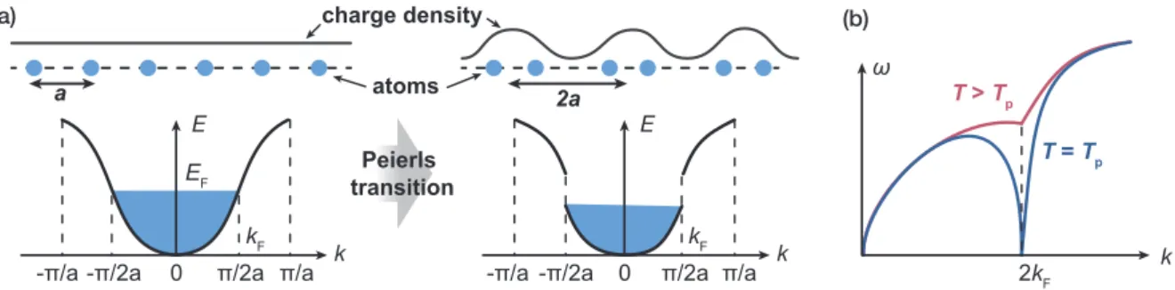
1.2 Spin and charge in one-dimensional solid state materials
A uniform spin(S)-1/2 chain with antiferromagnetic interaction can be mapped to a spinless, interacting fermion system by the Jordan-Wigner (J-W) transformation. Further-more, by bosonization, the fermion system can be mapped to a gapless boson system. The low-energy excitations are found to be topological S = 1/2 soliton excitations (spinons).
When the next nearest-neighbor interaction and dimerization are introduced into the
S = 1/2 antiferromagnetic spin chain, the system undergoes a phase transition and the
low-energy excitations of the system become gapped S = 1 soliton excitations. Since S = 1, the excitations are called triplons, which have triple degenerated spin quantum numbers. Besides one-dimensional spin systems, triplon appears in a two-dimensional dimer system and ladder systems as well. The first part of this dissertation focuses on triplon in terms of spin current carriers.
In this section, we introduce the bosonization of a one-dimensional fermion system and the Tomonaga-Luttinger liquid and describe the J-W transformation that connects the one-dimensional spin chain to the fermion system. Finally, we will describe a model involving frustration and dimerization in a one-dimensional spin chain.
1.2.1 One-dimensional fermion system
The free Fermi gas (such as electron gas) is transformed into a Fermi liquid when an inter-action is applied adiabatically to the system. There are two types of elementary excitations in the Fermi liquid at finite temperatures: collective excitations (plasmons) and individual excitations (quasi-particles). The dispersion relation of plasmons at long wavelengths in three dimensions is
ω2= ω2p+3! 2k2
Fq2
5m2 + o(q4). (1.17)
Here, ωp = (4πne2)1/2 is the plasma frequency. Furthermore, the dispersion relation of individual excitations in three-dimensions is a band at long wavelengths, and there is an energy gap between the plasmons, allowing us to clearly distinguish quasi-particles and collective excitations. The quasi-particle lifetime τk is calculated from the Green’s function, which gives[45]
1.2 Spin and charge in one-dimensional solid state materials 12 Here, ,k is the energy of quasi-particle and ,F is the Fermi energy. That is, the excitation of infinitesimal energies has an infinitely long lifetime and the Fermi liquid is stable within the energy range of ,k− ,F - τ−1. Thus, the low-energy behavior of the Fermi system with interactions in three dimensions can be explained by considering a quasi-particle picture.
On the other hand, the plasma oscillation in one dimension has a linear dispersion (ω = qv) and the energy gap is zero at long wavelengths. Furthermore, the dispersion relation of the individual excitations becomes ω = q2
2m ± qvF at long wavelengths, with the same linear dispersion as the plasma oscillations, and the energy gap becomes zero at q = 0. Thus, at low energies, the distinction between individual and collective excitations becomes indistinguishable, and a well-defined quasiparticle picture such as the three-dimensional one becomes untenable. It is the lifetime of quasiparticles that has thoroughly destroyed the one-dimensional Fermi liquid picture. Calculating the quasiparticle lifetime, as is the case in three dimensions, shows that the lifetime does not depend on the excitation energy, but is a constant. This eliminates the energy range in which the quasiparticle is stable. The results of both the excitation spectrum and the quasiparticle lifetimes show that the Fermi liquid theory fails in one dimension and a new model must be considered.
Tomonaga-Luttinger liquid
As a new model for one-dimensional fermion systems, consider the Tomonaga-Luttinger model as H = H0+ Hint =! k ξkc†kck+ 2L1 ! k,k!,q(=0 V(q)c†kc†k!ck!−qck+q, (1.19) where V (q) is two-particle interaction. As an approximation for low energy excitations, we assume a linear dispersion around the Fermi level, as shown in Fig.1.5. This model is called the Tomonaga-Luttinger model and can be exactly solved by Bosonization[46,47], and the solution is the well-known Tomonaga-Luttinger liquid (TLL).
The starting point for bosonization assumes that the fermion energy band near the Fermi level is nearly linear: ,k ∼ (|k| − kF)vF, where kF and vF are the Fermi wavenumber and Fermi velocity. The fermion operator can be divided into left and right moving branches as shown in Fig.1.5:
ck= ck,RΘ(k) + ck,LΘ(−k), (1.20)
1.2 Spin and charge in one-dimensional solid state materials 13 E k π/a -π/a 0 EF kF E k 0 EF kF -kF right-moving branch left-moving branch
Figure 1.5: Linear approximation of the band structure near the fermi level. Let’s introduce the fermion density operator as
ρR(q) = ! k>0 c†kck+q= ! k>0 c†k,Rck+q,R, (1.21) ρL(q) = ! k<0 c†kck+q= ! k<0 c†k,Lck+q,L. (1.22)
From the commutation relation of c/c†, it is easy to verify the commutation relation of ρ
obeys[46] [ρR(q), ρR(−q)] = δq,q!Lq 2π (1.23) [ρL(q), ρL(−q#)] = −δq,q!Lq 2π (1.24) [ρR(q), ρL(−q#)] = 0. (1.25) (1.26) These relations indicate the ρR and ρL represent two independent boson operators. And this is why the method is called bosonization.
Using ρR/L, we can rewrite the 1st and 2nd terms in the Eq.1.19as [46]
H = H0+ Hint; Where, (1.27) H0 = 2πvF L ! q>0 & ρR(−q)ρR(q) + ρL(q)ρL(−q) ' (1.28) Hint = 2L1 ! q(=0 V1 & ρL(q) + ρR(q) '& ρL(−q) + ρR(q) ' . (1.29)
Here, V1 ≡ V (0) − V (2kF). In the real space representation, the fermion density operators are (x ≡ j · a) ρR,L(x) = 1 L ! q(=0 eiqxρR,L(q) + ρ0 (1.30)
1.2 Spin and charge in one-dimensional solid state materials 14 (ρ0 is the background fermion density) and the commutation relations are
[ρR(x), ρR(x#)] = 2πi1 ∂ ∂xδ(x − x #) (1.31) [ρL(x), ρL(x#)] = 2πi1 ∂ ∂xδ(x − x #). (1.32)
If we introduced two field operators φ(x) and θ(x) as [48,49] 1
√
π∂xφ(x) ≡ ρR(x) + ρL(x) − (ρR,0+ ρL,0) (1.33)
−√1
π∂xθ(x) ≡ ρR(x) − ρL(x) − (ρR,0− ρL,0) (1.34)
It is also clear that form the commutation relation of ρR,L, we have
[∂xφ(x), ∂x!θ(x#)] = i∂xδ(x − x#) (1.35) and (define P (x) = ∂xθ(x))
[φ(x), P (x#)] = iδ(x − x#), [φ(x), φ(x#)] = [P (x), P (x#)] = 0 (1.36)
which means the field operators φ(x) and P (x) are canonical conjugate quantities. Finally, the Hamiltonian is transformed into
H = u 2 ˆ dx&KP(x)2+ 1 K ( ∂xφ(x))2 ' (1.37) K−1 =*1 + V1
πvF is the Tomonaga-Luttinger liquid (TLL) parameter and u = vF/K.
1.2.2 One-dimensional spin-1/2 system
The starting point of our discussion is the 1D S = 1/2 Heisenberg model (also called the XXX model). The Hamiltonian is defined as
Hs= J! i (Si· Si+1) = J 2 ! i (Si+Si−+1+ S+i+1Si−+ 2SizSiz+1), (1.38) where Sα
i is the α component of S = 1/2 spin on the i-th site, J > 0 is the exchange constant between the nearest-neighboring (NN) sites.
1.2 Spin and charge in one-dimensional solid state materials 15
Jordan-Wigner transformation
We can map this model to a spinless fermion model by performing the Jordan-Wigner (J-W) transformation: Szi = ni−12 (1.39) Si+= exp −iπ i−1 ! j=1 nj c†i (1.40) Si−= ciexp iπ i−1 ! j=1 nj , (1.41) where c†
i, ci are fermion creation/annihilation operator at the i-th site. The fermion par-ticle number operator is defined as ni ≡ c†ici. The phase factor exp
"
iπ/ij−1=1nj #
is known as string operators. Consider cjexp(iπnj), if the j-th site particle number is zero, cjexp(iπnj) =
cj × 1 = 0 = −cj; if the j-th site particle number is one, cjexp(iπnj) = cj × −1 = −cj. Thus, cjexp(iπnj) = −cj. Similarly, exp {iπnj} cj = cj. Therefore, it follows that
{exp(iπnj), cj} = cj − cj = 0 (1.42) and similarly, {exp(iπnj), c†j} = 0 (1.43) therefore, {exp(iπnj), c†l} = 0 (l < j) (1.44) [exp(iπnj), c†l] = 0 (l ≥ j). (1.45)
From the commutation relation of spin operators, it is easy to show the fermion operators obey fermionic commutation relations:
{ci, c†j} = δij, {ci†, c†j} = {ci, cj} = 0 (1.46) Since the fermion operator at each site contains the spin operator at all sites, the J-W transformation is a non-local transformation.
Let’s rewrite the Hamiltonian (Eq.1.38) by the fermion operators. The XY components are Sj+Sj−+1 = exp −iπ j−1 ! i=1 ni c†jcj+1exp iπ j ! i=1 ni (1.47) = c† jexp(iπnj)cj+1 = c†jcj+1 (1.48)
1.2 Spin and charge in one-dimensional solid state materials 16 and therefore the Hamiltonian after J-W transformation is
H= J 2 ! i 0 (c† ici+1+ c†i+1ci) + 2 1 ni−12 2 1 ni+1−12 23 , (1.49)
which means a 1D S = 1/2 system is equivalent to a spinless fermion system. Under Fourier transformation cj = √1 N ! k eikajck (1.50)
(a is the lattice constant), the Hamiltonian becomes
Hs=! k ,(k)c†kck+1 N ! k,k!,q V(q)c†k+qc†k!−qck!ck−1 N ! k,k!,q V(q)c†k+q±G/2c†k!−q±G/2ck!ck (1.51) where N is the total number of sites, G ≡ 2π/a is the reciprocal lattice vector. ,(k) and
V(k) are given as
,(k) = J(cos ka − 1) (1.52)
V(k) = J cos qa (1.53)
As in the previous section, the bosonization procedure leads to a sine-Gordon type Hamiltonian model[47,49,50,51]: Hs = ˆ dx 0 u 2π[KP (x)2+K1(∂xφ(x)) 2] + 2g2 (2πa)2 cos(4φ) 3 . (1.54)
The exact value of K and u are evaluated from Bethe ansatz[47] as: K = 1/2 and u =
Jπa/2, where a is the lattice constant. g2 ∝ −J < 0 is also evaluated exactly[52, 47],
and is a parameter representing the umklapp scattering process of the fermion after J-W transfermation. From the renormalization group theory[47], the last term ∝ cos(4φ) is marginal for the Heisenberg model. Thus we ignore this term for low energy excitation hereafter. Then, the Hamiltonian is exactly the same as TLL (Eq.1.37). Hence, this system is called Tomonaga-Luttinger spin liquid.
1.2.3 One-dimensional spin-1/2 system with frustration and dimerization
Based on the aforementioned Heisenberg model, the model of the spin Peierls phase of CuGeO3 (which will be discussed in detail in the following sections) also takes into account
the dimerization from the lattice deformation and next-nearest-neighbor (NNN) interaction. Let J(i, i + 1) be the exchange constant between i-th and (i + 1)-th site and assume the deformation is small, we can expand J(i, i + 1) as
1.3 Soliton excitation in one-dimensional spin chain: spinon and triplon 17
(a)
i-2
i-1
i
i+1
i+2
J
J
ui ui+1
ui-2 ui-1 ui+2
J (1-δ)
(b)
J (1+δ)
> 0 < 0
αJ
Figure 1.6: (a) Before deformation: J is uniform across the chain. (b) After deformation: bond-alternating model with modulating J. The next-nearest-neighbor interaction αJ is also considered.
where ui, a, J and λ are space coordinate displacement for i-th site, lattice constant, ex-change constant without deformation and a constant with quantize the strength of spin-lattice coupling. Therefore, the exchange term in Eq.1.38changes as
JSi· Si+1→ J 1 1 +λ(ui− ui+1) a 2 Si· Si+1 (1.56)
Assume for all sites, the displacement is the same (|ui− ui+1| has same value for any i), we can define a constant δ ≡ λ(ui− ui+1)/a and the Hamiltonian becomes
Hs−δ= J N ! i=1 [1 + (−1)i+1δ]S i· Si+1 (1.57)
We can further include the NNN interaction into the model as a parameter α:
Hs−δ−α= J N ! i=1 4 [1 + (−1)i+1δ]S i· Si+1+ αSi· Si+2 5 , (1.58)
where J > 0 and the NNN coupling parameter α ≥ 0 causes frustration. The bosonization procedure also leads to a sine-Gordon type Hamiltonian model[47,53] as
Hs−δ−α= ˆ dx 0 u 2π[KP (x)2+ K1(∂xφ(x)) 2] + 2g1
(2πa)2 sin(2φ) + (2πa)2g2 2 cos(4φ) 3
. (1.59)
With g1 ∝ δ. Here, different form Eq. 1.54, g2 ∝ J(α − αc) We call this model the the Heisenberg-δ-α model hereafter.
1.3 Soliton excitation in one-dimensional spin chain: spinon
and triplon
1.3.1 Ground state and the soliton excitation in the Heisenberg-δ-α model
The α-δ phase diagram of the Heisenberg-δ-α model is shown in Fig. 1.7. In the phase diagram, we show 5 regions, from a to e.
1.3 Soliton excitation in one-dimensional spin chain: spinon and triplon 18
δ
α
0.5 0.241 0 0 1 a b c d e × CuGeO3Figure 1.7: Phase diagram of the S = 1/2 dimer chain with frustration (the Heisenberg-δ-α model).
Heisenberg model
At point a, the model is the Heisenberg model and the system is a TLL. Hulthen solved this model in 1938[54]. The essence of his calculation is reviewed in Ref. [55]. The ground state is a non-magnetic state and the correlation function
SiαSjα ∼ (−1)
i−j(log |i − j|)1/2
|i − j| ; |i − j| - 1 (1.60)
shows a decaying long-range correlation. In other words, all spins form a quantum entangled macroscopic singlet with Stot =/iSi = 0 [56]. In the short range, the spin correlation is given by[54],[57]
%SiαSiα+1& ∼ −0.148 (1.61)
%SiαSiα+2& ∼ 0.06 (1.62)
which seems to have a short range antiferromagnetic configuration.
The spin excitation in 1D the Heisenberg model is spinon that carres 1/2 spin[58]. Spinons are similar to domain wall excitations in the Neel state. In the real space spinon separates two sections of the macroscopic singlet by a phase shift of π. In the Heisenberg model, the spinons are gapless excitations[56], which has been proven both experimentally and theoretically (see Fig.1.8a, b).
To see more qualitatively what spinon is, we return to Eq. 1.54. If the exchange inter-action in the z-direction is infinitesimally larger than the XY direction (Jz > Jxy), then the term of cos(4π) is relevant and the ground state is a Neel state. The exact one-dimensional system does not allow for long-range antiferromagnetic orders to occur. However, due to the presence of antiferromagnetic correlations over a long distance, a localized picture of the Neel state is valid. The following discussion is based on this Neel picture. If Jz = Jxy = J,
1.3 Soliton excitation in one-dimensional spin chain: spinon and triplon 19 ω πJ k π/a π/2a 0 πJ/2 des Cloizeaux-Pearson mode (a) (b)
Figure 1.8: (a) Spinon spectrum. (b) Inelastic neutron scattering result of the spinon spec-trum in CuSO4· 5D2O and a theoretical calculation involving multiple spinon dynamics[56].
but the local spinon picture is equivalent to that of the Neel state because of the short-range antiferromagnetic correlation is preserved. Therefore, taking into account the term of cos(4φ), the ground state of the lowest energy corresponds to cos(4φ) = 1 with φ = nπ
2. By
using field operators, the original spin operators are
Sjz = 1
π∂xφ+ (−1)
ja
1cos(2φ) + · · · (1.63)
Sj+= eiθ[b0(−1)j + b1cos(2φ) + · · · ]. (1.64)
Substituting φ = nπ/2 into them, we get Sz
j ∝ (−1)j and Sjz ∝ (−1)j+1. This means that the two Neel states are degenerate (Neel-a and Neel-b in Fig. 1.9).
Considering the excitation from the ground state, it corresponds to the φ kink between two ground states with ∆φ = ±π/2. Let’s look at the spin quantum number of the ex-citations. From δSz = 1
π ´∞
−∞dx∂xφ, we can see that the excitation of ∆φ = +π/2 (Fig.
1.9(b)) is a δSz = 1/2 spinon (soliton) and the excitation of ∆φ = −π/2 (Fig. 1.9(c)) is a δSz = −1/2 spinon (antisoliton). When considering the motion of spinon, the canonical equations show that the equation of motion of P (x) and φ(x) are
∂P(x) ∂t = − δH δφ(x) = u ∂2φ(x) ∂x2 ; (1.65) ∂φ(x) ∂t = + δH δP(x) = uP (x). (1.66)
Thus, φ(x) follows the wave-equation:
∂2φ(x) ∂t2 − u
2∂2φ(x)
∂x2 = 0. (1.67)
1.3 Soliton excitation in one-dimensional spin chain: spinon and triplon 20 (a) φ Neel-a Neel-b - cos ( )4φ Neel-a Neel-b π/2 0 π/4 0 π/2 0 φ (b) ∂xφ S = 1/2 x x Neel-a Neel-b spinon (soliton) S = 1/2 0 π/2 0 φ (c) ∂xφ S = -1/2 x x Neel-a Neel-b spinon (antisoliton) S = -1/2
Figure 1.9: (a) Degenerated Neel orders with respect to different φ values. (b) and (c): Schematic illustrations of spinon (soliton/anti-soliton) excitations.
As for the spectrum of spinon, the Heisenberg model for S = 1/2 can be solved rigor-ously by Bethe-ansatz[47], but it is mathematically complex and will not be discussed here. Instead, let’s consider the XY model of the z-direction exchange interaction Jz = 0 as:
HXY = J! i (Sx i · Six+1+ Siy· S y i+1) = J 2 ! i (S+ i Si−+1+ Si++1Si−). (1.68) The J-W transformation gives us a free fermion system with
H= J 2 ! i " c†ici+1+ c†i+1ci # . (1.69)
If we diagonalize it, we find that the spectrum of the fermion system is
,k = J cos(k). (1.70)
The ground state is the fully occupied state of particles with negative energy, as shown in Fig. 1.10, and the excited state is the magnon with δSz = ±1, which adds/eliminates one fermion to the positive/negative energy(see Eq. 1.39). However, the magnon is not the lowest excited state of the spin, it splits into two spinons with δSz = ±1/2. If we denote the wavenumber of the spinons as q1 and q2, we get a continuous spectrum as (also see Fig.
1.3 Soliton excitation in one-dimensional spin chain: spinon and triplon 21 k ε ( k ) 0 π/a -π/a π/2a -π/2a J -J ω J 2J q π/a -π/a -π/2a 0 π/2a
Figure 1.10: Left: band structure (ground state) of 1-D XY model. Right: excitation spectrum
1.10)
q= q1+ q2 (1.71)
ω(q) = J6sin(q1) + sin(q2)7. (1.72)
In the case of the Heisenberg model with Jz = Jxy, as mentioned above, the system is TLL, but the various concepts of free fermions are still applicable. The spinon excitation spectrum is the same form as Eq. 1.72, but the spinon velocity is replaced by u = Jπ/2, which is a renormalization value of the fermion interaction. The wavenumber dependence is shown in Figs. 1.8(a) and (b). We call the lowest limit of the continuous spectrum the des Cloizeaux-Pearson mode.
Heisenberg-α model
Consider the line of δ = 0 in Fig. 1.7. For α < αc = 0.241, g2 ∝ J(α − αc) < 0 and the cos(4φ) is marginal just as the Heisenberg hamiltonian (Eq. 1.54) and the spin chain is in the same universality class as the TL spin liquid: the ground state is non-magnetic spin liquid and the excitation is gapless spinon. For α > αc, the spin chain is in a dimerized state and the spin excitation is gapped triplon. At point α = 0.5, the exact ground state is very obvious: the hamiltonian is
H =! i (JSi· Si+1+ 0.5JSi· Si+2) (1.73) = J 2 ! i (Si· Si+1+ Si+1· Si+2+ Si· Si+2) (1.74) = J 4 ! i 0 (Si+ Si+1+ Si+2)2− 94 3 , (1.75)
1.3 Soliton excitation in one-dimensional spin chain: spinon and triplon 22 Dimer-a αJ αJ J J J J J αJ αJ Dimer-b
Figure 1.11: Uniform spin chain with NNN. For α > αc, there are two degenerated dimer ground states.
and to minimize the energy, at the ground state |Si+ Si+1+ Si+2| should be 1/2, which means two out of three spins coupled as a singlet. There are two degenerated ground states: dimer-a and dimer-b shown in Fig. 1.11. The translational invariant symmetry is broken and the excited states have an energy gap.
There are a gapless state at (α, δ) = (0, 0) and a gapped state at (α, δ) = (0.5, 0). This implies a phase transition at some point of α, which is the former mentioned αc = 0.241. The value of αc is numerically calculated[59]. For α > αc (g2 > 0) the cos(4φ) term is relevant. Even for δ = 0, the ground state dimerize spontaneously and an excitation gap open[59,60,61].
In this NNN induced gaped state, the ordered values of φ becomes φ = π/4 + nπ/2. This leads to a different spin configuration compare to the Heisenberg chain of φ = nπ/2. We can also define the dimer operators as[49]
(−1)j(Sx
jSjx+1+ SjySjy+1) ) dxysin(2φ) (1.76) (−1)jSz
jSjz+1 ) dzsin(2φ). (1.77)
Both dxy/z and a1, b0/1are constants that are numerically solvable[49]. Then, a spin dimer-ization occurs in this phase as:
%Sjx,y,zSjx,y,z+1 − Sjx,y,z+1 Sjx,y,z+2 & '= 0. (1.78) The two spin correlation function is also different from Heisenberg model. In the dimerized case, Sα
i Sjα decays exponentially, and the spins in the chain have locked themselves into singlet states.
1.3 Soliton excitation in one-dimensional spin chain: spinon and triplon 23
Heisenberg-δ model and the spin-Peierls transition
Consider the line of α = 0, δ > 0 in Fig. 1.7 (line b). The Hamiltonian is
Hs−δ = ˆ dx 0 u 2π[KP (x)2+K1(∂xφ(x)) 2] + 2g1 (2πa)2 sin(2φ) 3 . (1.79)
Here, we ignored the marginal term of cos(4φ). The sin(2φ) term is relevant even for infinitesimally small δ and the ordered value of φ is φ = −π/4 + nπ. From the expression of
Sz
j (Eq.1.63), we know that the dimer state corresponds to sin(2φ) = −1 and the Neel state corresponds to cos(2φ) = ±1. Thus, in this case, the ground state is a dimer state, and just as the α > αc, all spins are locked into singlet state: %Szj& = 0 and %S
x,y,z j S x,y,z j+1 − S x,y,z j+1 S x,y,z j+2 & '= 0.
This system has one important difference with the Tomonaga-Luttinger spin liquid and that is the quantum number of the spin excitations. In this case, the jump between to ordered φ is π and the spin of an excitation is now δSz = ±1. The plus and minus sign correspond to a soliton and antisoliton. There are other spin excitations call breathers (δSz = 0), which are the bound states of the soliton and antisoliton. For the Heisenberg-δ model (isotropic exchange interaction), the lightest breather has the same excitation gap as soliton and antisoliton[49]. Therefore, we can consider the soliton, antisoliton, and the lightest breather compose a triplet state (we can call it triplon excitation).
A schematic understanding of these excitations is given by Nakano & Fukuyama [62]. They also used the bosonized Hamiltonian, but with different coefficients due to the different definitions of some parameters. We will proceed with the discussion by using parameters defined in Ref.[49]. As shown in Fig. 1.12(a), there are four well-defined magnetic orders correspond to φ = −π
4 + nπ, nπ,π4 + nπ, and 3π4 + nπ. Referring to the definitions of Sjz (Eq.1.63) and dimer operator Eq. 1.77, it is easy to see that the above states are a low-energy dimer state (i.e. the ground state); a Neel state; a high-low-energy dimer, and another Neel state, respectively.
The soliton and anti-soliton excitations locate at the place where φ jumps between two Dimer-a states. The change in φ are ±π for the so liton/anti-soliton. Notice that S(x)z is proportional to the spatial derivative of φ, the total z-component of spin is Sz
tot ∼´ π1 dφ dxdx= ±1 for soliton/soliton. The lowest energy breather is a bound state of soliton and anti-soliton with Sz
tot = 0. Soliton (|↑↑&), anti-soliton (|↓↓&) and the lowest energy breather
((|↑↓& + |↓↑&)/2) degenerate and form the spin-1 triplet excitation (call triplon)[63,49]. The spectrum of triplon excitation is calculated numerically by Bonner et al.[63] We show the calculated spectrum in Fig. 1.13. The dispersion relation at low k can be expressed
1.3 Soliton excitation in one-dimensional spin chain: spinon and triplon 24 (a) φ Neel-a Neel-b Dimer a Dimer b Dimer a Dimer b Neel-a Neel-b -π/4 3π/4 0 φ 0 0 ∂xφ φ (b) (c) (d) -π/4 for δ>0 2 Dimer a ∂xφ φ ∂xφ S = 1 S = -1 S = 0 x x x x x x sin ( )2φ -π/4 3π/4 -π/4 3π/4 3π/4 π/4
Figure 1.12: (a) Four magnetic orders with respect to different φ values. Schematic illus-trations of (b) Soliton; (c) anti-soliton and (d) the lightest breather.
1.3 Soliton excitation in one-dimensional spin chain: spinon and triplon 25 k 0 π/2 π -π/2 -π δ=0 δ=1/3 δ=1/9
ε
3J f (δ)Ground state energy / J 0 0.02 0.04 0.06 0.08 0.1
2 4 6 ×10⁻² f (δ) = δ 2 lnδ f (δ) = δ2 ln2δ f (δ) = δ4/3
Figure 1.13: Reprinted from Bonner et al.[63] Left: spin excitation spectrum of the Heisenberg-δ model. Spin excitation are gapless for uniform chain (δ = 0) and gapped for deformed chains. Notice that the deformation shrinks the Brillouin zone to 1/2. Right: Calculated ground state energy v.s three functions of δ. The excitation gap is well fitted by
,gap∝ δ4/3.
as[64,63]
ω(k) ∼*∆2+ (ωM2 − ∆2) sin2(2πk) (1.80)
where ∆ is the energy gap and ωM is the maximum value of the energy. The energy gap ∆, on the other hand, is also calculated by Bonner et al.,[63] and is shown in the right panel of Fig. 1.13. In the figure, the calculated ground state energy is compared with three theoretical model: the XY model with (exact) ∆ ∝ δ2ln2δ, the Hartree-Fock theory by
Bulaevskii [65] with ∆ ∝ δ2ln δ, and the Cross-Fisher theory[66] with ∆ ∝ δ4/3. Obviously,
the Cross-Fisher theory matches the numerical result better.
Cross-Fisher theory[66] also shows the energy gap of the spin system. The energy gain by the spin system due to the emergence of spin gap is Espin∝ δ2/3, while the elastic energy
loss due to the lattice distortion is Eelastic∝ δ2 for small δ. Thus, in a spin-lattice coupled 1D Heisenberg spin chain (at 0 K), the lattice deforms spontaneously and the ground state becomes a bound-alternating chain. This phase transition form δ = 0 to δ > 0 is known as the spin-Peierls (SP) transition.
CuGeO3 as a example of Heisenberg-δ-α model
There is not a general solution for arbitrary values of (α, δ). Instead, I will focus on the model hamiltonian for CuGeO3 in the SP phase has parameter as (α, δ) = (0.36, 0.0022)
1.3 Soliton excitation in one-dimensional spin chain: spinon and triplon 26 20 Energy (meV) 10 0 T = 1.8 K k 0 π/4 π/2 0.5 2 1 3 Energy (meV) H (kOe) 0 20 40 60 80 100 T = 6 K
along the spin chain
Figure 1.14: Reprinted from Regnault et al.[64]. Left: The dispersion relation of triplet excitation in CuGeO3. Right: The Zeeman splitting of triplon under magnetic field.
The spin elementary excitation of CuGeO3 in the uniform phase is spinon, and a small
excitation gap exists due to α > αc. By a numerical calculation[69], the excitation gap is less than 10−2J ∼ 1.6 K for α ∼ 0.36 and can be ignored. The spin excitation spectrum
of CuGeO3 in the SP phase is obtained via the neutron scattering and ESR[64,67,70,71].
Here, I show the data from Regnault et al.[64] in Fig. 1.14. Due to non-negligible interchain interaction and large NNN, the actual dispersion relation deviated from the theoretical curve[63]. The gap at k = 0 and k = π/2 are also different. However, the triplet nature of the excitation is unchanged and shows Zeeman splitting under magnetic field[72,73].
Chapter 2
Experimental details
2.1 Sample fabrication and evaluation methods
2.1.1 Fabrication of CuGeO3 single crystal
Pure CuGeO3 samples and Zn-doped Cu1−xZnxGeO3 samples are fabricated by Prof.
Fujita and Mr. YiFei Tang of the IMR, Tohoku University. A traveling solvent floating zone method (TSFZ) is used for the fabrication of single crystalline CuGeO3. Fig. 2.1 shows a
schematic illustration of the TSFZ apparatus in the Fujita Lab. A polycrystalline feed rod is hung, and a seed crystal is placed at the bottom of it. Single crystals are grown by melting and recrystallizing a polycrystalline feed rod sample. The heat is supplied by two halogen lamps, which are focused by two elliptical mirrors and concentrated on the rod. The melting zone travels from the bottom to the top by sweeping the focus of light. Since the sample do not touch any other materials, the contamination of impurities due to container contact is limited. Also, by controlling the rotation speed of the sample rod and the sweeping speed of the floating zone, large single crystals with uniform composition can be obtained.
The actual fabrication procedure is as follows. Powder of GeO2 (4N) and CuO (3N) are
weighed to match the stoichiometric ratio of Ge and Cu. The powder is blended well in a crucible and then is baked at 850◦C for 12 hours in the air. The sample is pulverized and
mixed again with a mortar. The sample is then cold-pressed to form a rod. The rod is put into a Tammann tube and annealed in air at 750 ◦C for 3 hours in an electric furnace. A
hole is drilled on one side of the rod and the rod is further annealed for 12 hours in air at 950 ◦C. This rod is used as a feed rod in the TSFZ. For single crystal growth, the TSFZ
method is performed in air. For the first TSFZ, two feed rods are used both upper and lower shafts, and irregular crystals are obtained after the first TSFZ. A small regular piece of single crystal is cut off from the irregular crystal and used as a seed for the second TSFZ (as shown Fig. 2.1).
2.1 Sample fabrication and evaluation methods 28 Gold mirror lamp Feed rod Floating zone Single crystal Lower shaft Upper shaft
Figure 2.1: Schematic illustration of the floating zone apparatus.
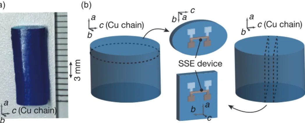
Single crystalline CuGeO3 prepared by a floating zone method is an elliptical cylinder
(see Fig. 2.2(a)) with the height of ∼ 15 mm (along the a-axis), the long axis of 7 mm (along the c-axis) and a short axis of 3 mm (along the b-axis). Crystal orientations are determined by using a Laue camara.
The single crystals are cut into different surfaces for SSE measurements. The CuGeO3
crystals are easily cleaved into the (100) plane, as illustrated in Fig. 2.2(b). The cleaved elliptical samples are used as a reference sample in on-chip SSE measurements. In the cleaved sample, the thermal gradient is applied perpendicular to the spin chain direction (c-axis). The cleaved (100) samples are also used in the non-local SSE measurements.
The main on-chip SSE measurements are performed in (001) oriented samples, in which the thermal gradient is applied parallel to the spin-chain. The single crystal is cut into the (001) surface and polished before device fabrication. First, the sample is mounted on the polishing fixture and then polished with water-proof polishing paper (3M corp.) with a grain size of #2000, #4000, and #10000 in order. This polishing is performed manually using a JEOL HLA-2 polishing machine. During polishing, water is poured on the polishing paper to prevent it from drying out. After that, we use an automatic polishing machine (Marutoh ML-150P, MKL-106) for fine polishing. Alumina suspension is used. The particle size of the alumina powder in the suspension is 1.0 µm, 0.1 µm, and 0.05 µm in order. Afterward,
2.1 Sample fabrication and evaluation methods 29 we clean the sample by a ultrasonic cleaner.
c b a c b a a b c (Cu chain) a b c (Cu chain) SSE device 3 mm a b c (Cu chain) (a) (b)
Figure 2.2: (a) Image of a CuGeO3 single crystal. (b) Schematic illustration of CuGeO3
sample cut into different crystalline orientation.
Figure 2.3(a) shows the results of atomic force microscopy (AFM) of the surface of as-cleaved CuGeO3 (100) surface. The surface are atomically smooth, with an arithmetical
mean deviation (Ra) less than 0.02 Å. We used the as-cleaved surface surface for
microfab-rication in the non-local SSE setups. The polished (001) surface, on the other hand, has a much larger Ra = 1.2 Å(see Fig. 2.3(b)). But this is still sufficiently small, compare with
2.1 Sample fabrication and evaluation methods 30
AFM: cut & polished 7 (nm) 0 2.2 (nm) 0 1 0.8 0.6 0.4 0.2 0 1 0.8 0.6 0.4 0.2 0 (μm) (μm) AFM: as-cleaved 0.5 0.4 0.3 0.2 0.1 0 0.5 0.4 0.3 0.2 0.1 0 (μm) (μm) (a) (b)
Figure 2.3: AFM image of (a) the as-cleaved (100) surface and (b) the polished (001) surface. We also performed a X-ray diffraction (XRD) measurement of a cleaved CuGeO3 (100)
sample. Fig. 2.4shows the XRD result of a 2θ scan. A peak at 2θ = 37◦, which corresponds
to (200), is clearly observed. The absence of other peaks of CuGeO3 indicates the sample
2.1 Sample fabrication and evaluation methods 31
45
40
35
25
2θ (deg)
50
55
Intensity
(10
4count
s)
30
60
65
70
X-ray
3
(200)
0
2
1
(300)
X-ray
(001)
(002)
0
0.2
0.4
0.6
0.8
(b)
(a)
Figure 2.4: XRD 2θ scan of (a) the as-cleaved (100) surface and (b) the (001) surface.
2.1.2 Magnetron sputtering
In this study, Pt, Au, NbN, and SiO2 films are prepared using magnetron sputtering.
Fig. 2.5is a schematic illustration of the sputtering apparatus. Before deposition, argon gas is introduced into the vacuum chamber at a constant flow rate. Then, A RF high voltage is applied between the substrate holder and the target, resulting in the ionization of argon atoms and the generation of plasma (which is trapped in a magnetic field) in the vicinity of the target. The high-energy argon ions accelerated by the large electric field collide with the target surface and knock out the target atoms. RF sputtering enables the fabrication of electrically insulating targets and high-melting-point targets, which cannot be grown by the vapor deposition method. The sputtering system used in this study consisted of four vacuum chambers: a load-lock chamber, a transfer chamber, a chamber for metals deposition, and a chamber for oxides deposition. The deposition conditions of the materials used in this
2.1 Sample fabrication and evaluation methods 32
Figure 2.5: Schematic illustration of magnetron sputtering apparatus. study are shown in table2.1.
The ferrimagnetic insulator Y3Fe5O12 (YIG) used as a reference sample is also prepared
by the sputtering method. Single crystals of the ferrimagnetic insulator Y3Fe5O12 with a
thickness of 40nm are grown on Gd3Ga5O12(111) substrates by magnetron sputtering[74].
Prior to the deposition, the Gd3Ga5O12substrates are annealed in air at 825◦C for 30 min,
in a face-to-face configuration. This pre-annealing process improved the crystallinity of Gd3Ga5O12 and the surface after annealing became a step-and-terrace structure. After the
deposition, the as-grown amorphous Y3Fe5O12 samples are post-annealed in a face-to-face
configuration for 200 sec at 825 ◦C in the air to crystallize.
Films RF power Flow rate of gasses Pressure Rate
Pt 20 W Ar/15 sccm 0.1 Pa 1.3 nm/min
YIG 150 W Ar/15 sccm and O2/0.3 sccm 0.1 Pa 0.2 nm/min
NbN 100 W Ar/15 sccm and N2/2 sccm 0.14 Pa 2.55 nm/min
SiO2 130 W Ar/15 sccm and O2/3 sccm 1 Pa 0.6 nm/min
Au 20 W Ar/15 sccm 0.7 Pa 13.2 nm/min
2.1 Sample fabrication and evaluation methods 33
2.1.3 Electron beam lithography
In this study, we combined electron beam lithography (EBL) and the lift-off process to fabricate micro- and nano- scale patterns. The process of nano-pattering by the lift-off method is shown in Fig. 2.6 and the detail of each step is as follow.
• Resist preparing: First, the MMA polymer resist is spin-coated at 4000 rpm for 1 minute and pre-baked at 150 C◦ for 3 minutes. Next, the second layer of PMMA950
A2 resist is spin-coated at 3000 rpm for 1 minute and pre-baked at 150 C◦for 3 minutes
in the same way. The thickness of the resist is measured as 400 nm with a Dektak surface step profiler. Since the sample is insulating, a conductive layer must be made over the resist to avoid the charging up effect of electrons during the lithography. A water-based conductive polymer (ESPACER 300; Showa Denko, inc.) is spin-coated at 3000 rpm for 1 minute on top of PMMA. We do not pre-bake the ESPACER. • Exposure: The sample is transferred to an EB lithography chamber and irradiated
with an electron beam. The ELS-7500 (Elionix, inc.) with an acceleration voltage of 50 kV is used for lithography. The exposure dose is optimized to 5.5µC/cm2 for our
resist. With this dose, the dose time setting is different for different beam currents. We use a smaller beam current (100 pA) for fine structures, such as the platinum wire for ISHE detection, and a larger beam current (500 pA) for large structures, such as the outer contacts.
• Development: A mixture of methyl isobutyl ketone (MIBK) and isopropanol (IPA) in a 1:3 ratio is used as the developer. Samples are first immersed in this developer for 30 seconds to dissolve the exposed resist and then rinsed with IPA for 30 seconds. The sample is blown with nitrogen gas to remove the organic residue.
• Deposition and lift-off: Due to the different sensitivity to the electron beam, the cross-section of the resist has an inverted taper profile, as shown in Fig.2.6f. A layer of metal is then deposited on the sample. After deposition, the remaining resist is removed by ultrasonic cleaning with acetone (100 kHz) for approximately 10 seconds.
2.2 Measurement methods 34
MMA
(a)
(b)
(f)
(i)
(e)
Electron beam
PMMA A2
(c)
(d)
(g)
(h)
lift-off
Deposition
Figure 2.6: Schematic illustration of the lift-off processes. (a) Spin-coating of the first layer of resist (MMA). (b) Baking. (c) Spin-coating of the second layer of resist (PMMA A2) (d) Baking. (e) EB exposure. (f) Development of patterns. (g) Deposition of film. (h) Lift-off. (i) Microfabricated sample.
2.2 Measurement methods
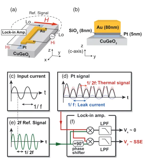
Cryostats and superconducting magnetsTransport measurements are performed on a physical properties measurement system (PPMS; Quantum Design, Inc., as shown in Fig. 2.7(a)). This system is capable of mea-suring over a temperature range of 1.9 K to 400 K. At low temperatures, it can stabilize the temperature with high accuracy, typically within ∼ 1 mK. The PPMS can also supply a uniaxial magnetic field perpendicular to the floor up to ±14 T. All transport measurements are performed by a rotator option. Samples are mounted on a PPMS rotator option chip (see Fig. 2.7(c)) with GE varnish and attached to a rotator rod. The electrical connections from the sample to the chip are made via Au wires. By using different chips, we are capable to measure both in-plane and out-of-plane magnetic field angular dependence.
The PPMS has a variety of built-in options, including DC/AC resistivity measurements and Hall effect measurements, but to perform more complex experiments, we built a remote measurement system[75]. A PPMS controller PC (with a control program called MultiView; Quantum Design, Inc.) is connected to a remote PC, where it runs a user-written MATLAB (version R2018a; MathWorks, Inc.) measurement control program via a LAN cable. It then remotely sends temperature and magnetic field control commands to the MultiView program. Meanwhile, other external measuring instruments connected to the sample via
2.2 Measurement methods 35 PPMS probe 2.5 cm PPMS probe inserted through top of dewar Magnet protection circuit 9 or 14 tesla magnet L. N2 reservoir High-Tc magnet leads L. He reservoir Magnet Thermometer Sealed sample space Cooling annulus
Puck Heaters and thermometers
Dual impedance system (a)
(c)
PPMS
Sample Driving linear motor
Detection coilset (b) (1) (2) Rotator chips Rotator rod Rotator motor Inserted into
the PPMS probe Magnetic
field (positive)
Figure 2.7: Cryostats and magnets used in this study. (a) Sectional view of the PPMS and sample probe[76] (b) VSM option of the PPMS. (a) and (b) are cited from the homepage of Quantum design, inc. (c) Rotator option of the PPMS. There have two kinds of rotator chips: (1) for the in-plane magnetic field rotation, (2) for the out-of-plane field rotation.
![Figure 1.3: (a) Detection of ISHE signal in a non-local nano-device[12]. (b) ISHE signal detection under FMR[13]](https://thumb-ap.123doks.com/thumbv2/123deta/5888894.1047712/10.892.212.697.262.897/figure-detection-ishe-signal-local-device-signal-detection.webp)


![Figure 2.7: Cryostats and magnets used in this study. (a) Sectional view of the PPMS and sample probe[76] (b) VSM option of the PPMS](https://thumb-ap.123doks.com/thumbv2/123deta/5888894.1047712/39.892.141.842.195.894/figure-cryostats-magnets-study-sectional-ppms-sample-option.webp)