FPGAの消費電力を削減するHDLコーディング手法の検討
2
0
0
全文
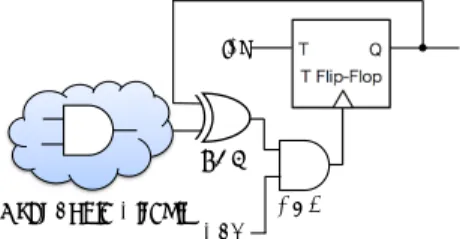
(2) 情報処理学会第 76 回全国大会. D Q D Flip-Flop. XOR. cnt[0] XOR. CLK. D Q D Flip-Flop. cnt[1]. XOR. CLK. D Q D Flip-Flop. 600 cnt[n-1]. Power Consumption[mW]. ʻ1ʼ. 500. CLK. 400. a. n-bit counter ʻ1ʼ ʻ1ʼ. XOR. D Q D Flip-Flop. CLK. T Q T Flip-Flop. cnt[0] ʻ1ʼ. T Q T Flip-Flop. cnt[1]. ʻ1ʼ. T Q T Flip-Flop. cnt[n-1]. 200 100. Q. CLK. 165%. 300. AND. 0. AND. Normal. Employing prioir work. b. n-bit counter employing prior work. Figure 5: Power consumption of the normal two 1000Figure 3: Test circuits with and without the new cod- bit counters and the two 1000-bit counters employing ing style in the prior work. prior work. !""#$%!"#$%&"!&!'(#)!'!(#*!'!&+$,-.! !()!*"!/'+,"-.$-!0&1-!/-$#%! !!!!#0!'"#$%&"-!,+23!1&!,$3$.! -%.!. DATA IN1 IN2 LOAD CLK. D Q D Flip-Flop CE. ENABLE. Recommended coding style. DOUT. !""#$%!4$3"0&1!&!'(#)!'!(#*!'!0&1-.! !()!*"!/'+,"-.$-!4$3"0&1-!/-$#%! !!!!#0!'&+$,-!,+23!1&!,$3$.! -%.!. DATA LOAD IN1 IN2 CLK. D Q D Flip-Flop CE. DOUT. ENABLE Not recommended coding style. Figure 6: Recommended and not recommended coding styles. ferent clock per FF. Figure 4: Measurement of power consumption by It is not necessarily good to gate the clock port, Adept2.13.1 software system. because gated clocks can increase clock delay, clock skew, and cause glitches and other undesirable effects. work” represents power consumption of the two 1000- From these reasons, Xilinx recommends using the dedbit counters with the new coding style. The normal cir- icated clock-enable (CE) port instead of gating the cuit consumes 213mW, the circuit employing the prior clock port [4]. Figure 6 shows recommended and not work consumes 564mW and 165% higher than Normal. recommended coding styles by Xilinx. Using the clock In the next section, we discuss the reason why the new enable can improve timing characteristics and analysis coding style does not achieve lower power consumption. of the design. Therefore, it is promising to use clock enable. 4 Discussion and Summary In the future work, it is crucial to seek better HDL Implemented circuits on Xilinx FPGA Spartan-6 coding styles based on obtained findings from this exconsist of configurable logic blocks (CLBs) and switch amination. matrixes connecting between CLBs. A CLB has logic cells, called ”Slices”, and each slice has Lookup Ta- References bles (LUTs), Flip-Flops (FFs), and single clock input [1] Thomas Marconi, Dimitris Theodoropoulos, Koen Bertels, and Georgi Gaydadjiev. A Novel HDL Coding Style port [3]. LUTs are used to realize combinational logic to Reduce Power Consumption for Reconfigurable Decircuits, and FFs are used to realize sequential logic vices. In Jinian Bian, Qiang Zhou, Peter Athanas, Yacircuits. jun Ha, and Kang Zhao, editors, FPT, pp. 295–299. In our test circuit with the new coding style, differIEEE, 2010. ent clock per FF is fed the clock input. Since each slice has single clock input port, the Xilinx logic synthesis [2] Saeyang Yang. Logic Synthesis and Optimization tool cannot place the FFs fed with such different clocks Benchmarks User Guide Version 3.0, 1991. in the same slice. In fact, the occupied slice ratio of [3] 7 Series FPGAs Configurable Logic Block User Guide. Employ prior work is 29 % while that of Normal is http://www.xilinx.com/support/documentation/ 11%. This causes the increase of the number of the user guides/ug474 7Series CLB.pdf. occupied slices. The more the number of switch ma[4] HDL Coding Practices to Accelerate Design Perfortrixes increases, the higher the power consumption of mance. the FPGA is. Therefore, it is better to use coarse-grain http://www.eng.utah.edu/∼cs3710/xilinx-docs/ approach like feeding different clock per 32-bit register wp231.pdf. rather than to use fine-grain approach like feeding dif-. 1-26. Copyright 2014 Information Processing Society of Japan. All Rights Reserved..
(3)
図

関連したドキュメント
The author, with the aid of an equivalent integral equation, proved the existence and uniqueness of the classical solution for a mixed problem with an integral condition for
Now we are going to construct the Leech lattice and one of the Niemeier lattices by using a higher power residue code of length 8 over Z 4 [ω].. We are going to use the same action
Greenberg and G.Stevens, p-adic L-functions and p-adic periods of modular forms, Invent.. Greenberg and G.Stevens, On the conjecture of Mazur, Tate and
Then it follows immediately from a suitable version of “Hensel’s Lemma” [cf., e.g., the argument of [4], Lemma 2.1] that S may be obtained, as the notation suggests, as the m A
The proof uses a set up of Seiberg Witten theory that replaces generic metrics by the construction of a localised Euler class of an infinite dimensional bundle with a Fredholm
Using the batch Markovian arrival process, the formulas for the average number of losses in a finite time interval and the stationary loss ratio are shown.. In addition,
[Mag3] , Painlev´ e-type differential equations for the recurrence coefficients of semi- classical orthogonal polynomials, J. Zaslavsky , Asymptotic expansions of ratios of
We link together three themes which had remained separated so far: the Hilbert space properties of the Riemann ze- ros, the “dual Poisson formula” of Duffin-Weinberger (also named by
