EFM32 Gecko ファミリーEFM32PG12
ファミリ・データ・シート
EFM32 Gecko MCU は、世界で最もエネルギー効率に優れたマ
イクロコントローラです。
EFM32PG12 は、強力な 32 ビット ARM® Cortex®-M4 と、独自の暗号化ハードウェア・エ ンジン、セキュリティ管理ユニット、真の乱数発生器、および堅固な静電容量式タッチ・ センス・ユニットを含む広範なペリフェラルを特徴としています。これらの特徴に加え、 超低消費電流のアクティブ・モードおよびスリープ・モードを提供する EFM32PG12 マイ クロコントローラは、あらゆるバッテリ式アプリケーション、および高性能、低消費電 力を必要とするその他のシステムに適しています。 アプリケーション例: 省エネ機能 • ARM Cortex-M4、40 MHz • 超低エネルギー動作: • 0.39 μA EM4H ハイバーネート電流 • 1.5 μA EM2 ディープ・スリープ電流 (状態および RAM を保持しながら RTCC を実行) • 64 μA/MHz EM0 アクティブ電流 • ハードウェア暗号化エンジン(AES、ECC、 および SHA)および TRNG • セキュリティ管理ユニット (SMU) • 自律低エネルギー・センサー・インターフ ェイス (LESENSE) • ADC、VDAC、OPAMP、および静電容量式セン スなどの豊富なアナログ機能 • 統合された DC-DC コンバータ • 5 V トレラント I/O • IoT デバイスおよびセンサー • ヘルスおよびフィットネス • スマート・アクセサリ • ホーム・オートメーションおよびセキュリティ • 工業および工場オートメーション
Peripheral Reflex System 32-bit bus Core / Memory
ARM CortexTM M4 processor
with DSP extensions, FPU and MPU
Timers and Triggers
CRYOTIMER
Real Time Counter and Calendar Timer/Counter Low Energy Timer
Pulse Counter Watchdog Timer
Lowest power mode with peripheral operational:
Energy Management Brown-Out Detector DC-DC Converter Voltage
Regulator Voltage Monitor Power-On Reset Clock Management High Frequency Crystal Oscillator Low Frequency Crystal Oscillator Low Frequency RC Oscillator High Frequency RC Oscillator with DPLL Ultra Low Frequency RC Oscillator Auxiliary High Frequency RC Oscillator Serial Interfaces USART
Low Energy UARTTM
I2C
I/O Ports
External Interrupts
General Purpose I/O
Pin Reset Pin Wakeup
Low Energy Sensor Interface ETM Debug Interface RAM Memory ControllerLDMA
Flash Program Memory Analog Interfaces ADC IDAC Analog Comparator VDAC Capacitive Sense Op-Amp Other CRYPTO CRC True Random Number Generator SMU
第 1 章 機能リスト
EFM32PG12 の主な特徴は以下の通りです。 • ARM Cortex-M4 CPU プラットフォーム
• 高性能 32 ビット・プロセッサ、最大 40 MHz • DSP 命令のサポートおよび浮動小数点演算ユニット • メモリ保護ユニット • ウェイクアップ割り込みコントローラ • 柔軟なエネルギー管理システム • 64 μA/MHz、アクティブ・モード (EM0)
• 2.1 μA EM2 ディープ・スリープ電流(256 kB RAM 保持お よび LFXO から RTCC を実行)
• 1.5 μA EM2 ディープ・スリープ電流(16 kB RAM 保持およ び LFRCO から RTCC を実行)
• 1.81 μA EM3 ストップ電流(状態/256 kB RAM 保持および ULFRCO から CRYOTIMER を実行)
• 0.39 μA EM4H ハイバーネート・モード(128 バイトの RAM 保持) • 最大 1024 kB のフラッシュ・プログラム・メモリ • 書き込み中の読み出しが可能なデュアル・バンクを使用 • 最大 256 kB の RAM データ・メモリ • 最大 65 個の汎用 I/O ピン • プッシュプル、オープンドレイン、プルアップ/ダウン、入 力フィルタ、ドライブ強度を構成可能 • ペリフェラルの I/O 場所を構成可能 • 非同期外部割込み • シャットオフ・モードから出力状態を保持してウェイクアッ プ • ハードウェア暗号化 • AES 128/256 ビット・キー • ECC B/K163、B/K233、P192、P224、P256
• SHA-1 および SHA-2(SHA-224 および SHA-256) • 真の乱数発生器 (TRNG) • セキュリティ管理ユニット (SMU) • オンチップ・ペリフェラルへのきめ細かいアクセス・コント ロール • タイマ/カウンタ • 2 × 16 ビット・タイマ/カウンタ • 3 または 4 コンペア/キャプチャ/PWM チャンネル • 2 × 32 ビット・タイマ/カウンタ • 3 または 4 コンペア/キャプチャ/PWM チャンネル • 1 × 32 ビット・リアルタイム・カウンタおよびカレンダー • 1 × 32 ビット超低エネルギー CRYOTIMER によるエネルギ ー・モードからの定期的なウェイクアップ • 16 ビット低エネルギー・タイマによる波形生成 • 3 × 16 ビット・パルス・カウンタ、非同期オペレーション 可能 • 2 × 専用 RC 発振器付き監視タイマ • 8 チャンネル DMA コントローラ • 12 チャンネル・ペリフェラル・リフレックス・システム (PRS) による内部機器とペリフェラルの自律性信号への対応 • 通信インターフェイス • 4 × 汎用同期/非同期レシーバ/トランスミッタ • UART/SPI/SmartCard (ISO 7816)/IrDA/I2S/LIN
• トリプル・バッファ方式の全二重/半二重動作、フロー制 御付き • 低エネルギー UART • ディープ・スリープ・モードでの DMA による自律的動作 • 2 × SMBus サポート付き I2C インターフェイス • EM3 ストップ・モードでのアドレス認識 • 超低消費電力かつ高精度のアナログ・ペリフェラル • 12 ビット 1 Msps SAR アナログ・デジタル・コンバータ (ADC) • 2 × アナログ・コンパレータ (ACMP) • 2 × 12 ビット 500 ksps デジタル・アナログ・コンバー タ (VDAC) • 3 × オペアンプ (OPAMP) • デジタル・アナログ電流コンバータ (IDAC) • マルチチャンネル静電容量式センス・インターフェイス (CSEN) • 最大 54 ピンをアナログ・チャンネル (APORT) に接続し、 アナログ・ペリフェラル間で共有 • 低エネルギー・センサー・インターフェイス (LESENSE) • ディープ・スリープ・モードでの自律的なセンサー監視 • LC センサーや静電容量式タッチ・スイッチなど、幅広いセ ンサーをサポート • 最大 16 チャンネル • 超高効率パワー・オン・リセット(POR)および電圧降下検出器 • デバッグ・インターフェイス • 2 ピン・シリアル・ワイヤ・デバッグ・インターフェイス • 1 ピン・シリアル・ワイヤ・ビューワ • JTAG(プログラミングのみ) • エンベデット・トレース・マクロセル (ETM) • 広範な動作範囲 • 1.8 V ~ 3.8 V の単一電源 • 統合 DC-DC、最小 1.8 V の出力と最大 200 mA の負荷電流 (システム用) • 標準(-40 °C ~ 85 °C TAMB)および拡張(-40 °C ~ 125 °C TJ)温度グレードを利用可能 • パッケージ • 7 mm × 7 mm QFN48 • 7 mm × 7 mm BGA125 • 事前プログラム済み UART ブートローダ • ソフトウェア・フルサポート
2. Ordering Information
Table 2.1. Ordering Information
Ordering Code
Flash
(kB) RAM (kB)
DC-DC
Con-verter GPIO Package Temp Range
EFM32PG12B500F1024GL125-C 1024 256 Yes 65 BGA125 -40 to +85°C EFM32PG12B500F1024IL125-C 1024 256 Yes 65 BGA125 -40 to +125°C EFM32PG12B500F1024GM48-C 1024 256 Yes 33 QFN48 -40 to +85°C EFM32PG12B500F1024IM48-C 1024 256 Yes 33 QFN48 -40 to +125°C
EFM32
1
B
F
G
–
R
Tape and Reel (Optional) Revision
Pin Count Package – M (QFN)
Flash Memory Size in kB Memory Type (Flash)
Feature Set Code
G
J
500
1024
M 48
Temperature Grade – G (-40 to +85 °C), I (-40 to +125 °C)
Performance Grade – P (Performance), B (Basic), V (Value)
Family – J, P Series
Energy Friendly Microcontroller 32-bit Gecko
A
2
Device Configuration
1. Feature List . . . 2
2. Ordering Information . . . 3
3. System Overview . . . 7
3.1 Introduction . . . 7
3.2 Power . . . 8
3.2.1 Energy Management Unit (EMU) . . . 8
3.2.2 DC-DC Converter
. . . 8
3.2.3 Power Domains . . . 8
3.3 General Purpose Input/Output (GPIO) . . . 9
3.4 Clocking . . . 9
3.4.1 Clock Management Unit (CMU) . . . 9
3.4.2 Internal and External Oscillators. . . 9
3.5 Counters/Timers and PWM . . . 9
3.5.1 Timer/Counter (TIMER)
. . . 9
3.5.2 Wide Timer/Counter (WTIMER) . . . 9
3.5.3 Real Time Counter and Calendar (RTCC) . . . 9
3.5.4 Low Energy Timer (LETIMER) . . . .10
3.5.5 Ultra Low Power Wake-up Timer (CRYOTIMER) . . . .10
3.5.6 Pulse Counter (PCNT) . . . .10
3.5.7 Watchdog Timer (WDOG) . . . .10
3.6 Communications and Other Digital Peripherals . . . .10
3.6.1 Universal Synchronous/Asynchronous Receiver/Transmitter (USART) . . . .10
3.6.2 Low Energy Universal Asynchronous Receiver/Transmitter (LEUART) . . . .10
3.6.3 Inter-Integrated Circuit Interface (I
2C) . . . .10
3.6.4 Peripheral Reflex System (PRS)
. . . .10
3.6.5 Low Energy Sensor Interface (LESENSE) . . . .11
3.7 Security Features . . . .11
3.7.1 General Purpose Cyclic Redundancy Check (GPCRC) . . . .11
3.7.2 Crypto Accelerator (CRYPTO) . . . .11
3.7.3 True Random Number Generator (TRNG) . . . .11
3.7.4 Security Management Unit (SMU) . . . .11
3.8 Analog. . . .11
3.8.1 Analog Port (APORT) . . . .11
3.8.2 Analog Comparator (ACMP) . . . .11
3.8.3 Analog to Digital Converter (ADC) . . . .12
3.8.4 Capacitive Sense (CSEN) . . . .12
3.8.5 Digital to Analog Current Converter (IDAC) . . . .12
3.10.3 Linked Direct Memory Access Controller (LDMA)
. . . .13
3.10.4 Bootloader . . . .13
3.11 Memory Map . . . .14
3.12 Configuration Summary
. . . .16
4. Electrical Specifications
. . . 17
4.1 Electrical Characteristics
. . . .17
4.1.1 Absolute Maximum Ratings . . . .17
4.1.2 Operating Conditions . . . .18
4.1.3 Thermal Characteristics . . . .20
4.1.4 DC-DC Converter
. . . .21
4.1.5 Current Consumption . . . .23
4.1.6 Wake Up Times . . . .28
4.1.7 Brown Out Detector (BOD) . . . .29
4.1.8 Oscillators . . . .30
4.1.9 Flash Memory Characteristics . . . .34
4.1.10 General-Purpose I/O (GPIO) . . . .35
4.1.11 Voltage Monitor (VMON) . . . .37
4.1.12 Analog to Digital Converter (ADC)
. . . .38
4.1.13 Analog Comparator (ACMP)
. . . .40
4.1.14 Digital to Analog Converter (VDAC) . . . .43
4.1.15 Current Digital to Analog Converter (IDAC)
. . . .46
4.1.16 Capacitive Sense (CSEN) . . . .48
4.1.17 Operational Amplifier (OPAMP) . . . .50
4.1.18 Pulse Counter (PCNT) . . . .53
4.1.19 Analog Port (APORT) . . . .53
4.1.20 I2C . . . .54
4.1.21 USART SPI . . . .57
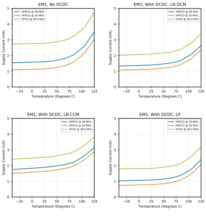
4.2 Typical Performance Curves . . . .58
4.2.1 Supply Current
. . . .59
4.2.2 DC-DC Converter
. . . .64
5. Typical Connection Diagrams
. . . 66
5.1 Power . . . .66
5.2 Other Connections. . . .66
6. Pin Definitions . . . 67
6.1 EFM32PG12B5xx in BGA125 Device Pinout . . . .67
6.2 EFM32PG12B5xx in QFN48 Device Pinout . . . .71
6.3 GPIO Functionality Table . . . .73
6.4 Alternate Functionality Overview . . . .92
6.5 Analog Port (APORT) Client Maps
. . . .104
7.3 BGA125 Package Marking . . . 117
8. QFN48 Package Specifications. . . 118
8.1 QFN48 Package Dimensions
. . . 118
8.2 QFN48 PCB Land Pattern
. . . .120
8.3 QFN48 Package Marking
. . . .122
9. Revision History
. . . .123
3. System Overview
3.1 Introduction
The EFM32PG12 product family is well suited for any battery operated application as well as other systems requiring high performance and low energy consumption. This section gives a short introduction to the MCU system. The detailed functional description can be found in the EFM32PG12 Reference Manual.
A block diagram of the EFM32PG12 family is shown in Figure 3.1 Detailed EFM32PG12 Block Diagram on page 7. The diagram shows a superset of features available on the family, which vary by OPN. For more information about specific device features, consult
Ordering Information.
Analog Peripherals
Clock Management
HFRCO + DPLL
IDAC
ARM Cortex-M4 Core
Up to 1024 KB ISP Flash Program Memory Up to 256 KB RAM A H B Watchdog Timer RESETn Digital Peripherals Input Mux Port Mapper Port I/O Configuration
Analog Comparator 12-bit ADC Temp Sense VDD Internal Reference IOVDD AUXHFRCO LFXO ULFRCO HFXO
Memory Protection Unit
LFRCO A P B LDMA Controller + -APORT
Floating Point Unit
Energy Management DVDD VREGVDD VREGSW bypass AVDD_0 AVDD_1 DECOUPLE IOVDD Voltage Monitor VDAC + -Op-Amp Capacitive Sense LESENSE CRC CRYPTO I2C LEUART USART RTC / RTCC PCNT CRYOTIMER TIMER LETIMER Port K Drivers PKn Port J Drivers PJn Port I Drivers PIn Port F Drivers PFn Port D Drivers PDn Port C Drivers PCn Port B Drivers PBn Port A Drivers PAn Mux & FB HFXTAL_P HFXTAL_N LFXTAL_P LFXTAL_N Voltage Regulator DC-DC Converter Brown Out / Power-On Reset Reset Management Unit Debug Signals (shared w/GPIO) Serial Wire and ETM Debug / Programming
3.2 Power
The EFM32PG12 has an Energy Management Unit (EMU) and efficient integrated regulators to generate internal supply voltages. Only a single external supply voltage is required, from which all internal voltages are created. An optional integrated DC-DC buck regulator can be utilized to further reduce the current consumption. The DC-DC regulator requires one external inductor and one external capaci-tor.
The EFM32PG12 device family includes support for internal supply voltage scaling, as well as two different power domains groups for peripherals. These enhancements allow for further supply current reductions and lower overall power consumption.
AVDD and VREGVDD need to be 1.8 V or higher for the MCU to operate across all conditions; however the rest of the system will operate down to 1.62 V, including the digital supply and I/O. This means that the device is fully compatible with 1.8 V components. Running from a sufficiently high supply, the device can use the DC-DC to regulate voltage not only for itself, but also for other PCB components, supplying up to a total of 200 mA.
3.2.1 Energy Management Unit (EMU)
The Energy Management Unit manages transitions of energy modes in the device. Each energy mode defines which peripherals and features are available and the amount of current the device consumes. The EMU can also be used to turn off the power to unused RAM blocks, and it contains control registers for the DC-DC regulator and the Voltage Monitor (VMON). The VMON is used to monitor multi-ple supply voltages. It has multimulti-ple channels which can be programmed individually by the user to determine if a sensed supply has fallen below a chosen threshold.
3.2.2 DC-DC Converter
The DC-DC buck converter covers a wide range of load currents and provides up to 90% efficiency in energy modes EM0, EM1, EM2 and EM3, and can supply up to 200 mA to the device and surrounding PCB components. Protection features include programmable current limiting, short-circuit protection, and dead-time protection. The DC-DC converter may also enter bypass mode when the input voltage is too low for efficient operation. In bypass mode, the DC-DC input supply is internally connected directly to its output through a low resistance switch. Bypass mode also supports in-rush current limiting to prevent input supply voltage droops due to excessive out-put current transients.
3.2.3 Power Domains
The EFM32PG12 has two peripheral power domains for operation in EM2 and lower. If all of the peripherals in a peripheral power do-main are configured as unused, the power dodo-main for that group will be powered off in the low-power mode, reducing the overall cur-rent consumption of the device.
Table 3.1. Peripheral Power Subdomains
Peripheral Power Domain 1 Peripheral Power Domain 2
ACMP0 ACMP1 PCNT0 PCNT1 ADC0 PCNT2 LETIMER0 CSEN LESENSE DAC0 APORT LEUART0 - I2C0 - I2C1 - IDAC
3.3 General Purpose Input/Output (GPIO)
EFM32PG12 has up to 65 General Purpose Input/Output pins. Each GPIO pin can be individually configured as either an output or input. More advanced configurations including open-drain, open-source, and glitch-filtering can be configured for each individual GPIO pin. The GPIO pins can be overridden by peripheral connections, like SPI communication. Each peripheral connection can be routed to several GPIO pins on the device. The input value of a GPIO pin can be routed through the Peripheral Reflex System to other peripher-als. The GPIO subsystem supports asynchronous external pin interrupts.
3.4 Clocking
3.4.1 Clock Management Unit (CMU)
The Clock Management Unit controls oscillators and clocks in the EFM32PG12. Individual enabling and disabling of clocks to all periph-erals is performed by the CMU. The CMU also controls enabling and configuration of the oscillators. A high degree of flexibility allows software to optimize energy consumption in any specific application by minimizing power dissipation in unused peripherals and oscilla-tors.
3.4.2 Internal and External Oscillators
The EFM32PG12 supports two crystal oscillators and fully integrates four RC oscillators, listed below.
• A high frequency crystal oscillator (HFXO) with integrated load capacitors, tunable in small steps, provides a precise timing refer-ence for the MCU. Crystal frequencies in the range from 38 to 40 MHz are supported. An external clock source such as a TCXO can also be applied to the HFXO input for improved accuracy over temperature.
• A 32.768 kHz crystal oscillator (LFXO) provides an accurate timing reference for low energy modes.
• An integrated high frequency RC oscillator (HFRCO) is available for the MCU system. The HFRCO employs fast startup at minimal energy consumption combined with a wide frequency range. When crystal accuracy is not required, it can be operated in free-run-ning mode at a number of factory-calibrated frequencies. A digital phase-locked loop (DPLL) feature allows the HFRCO to achieve higher accuracy and stability by referencing other available clock sources such as LFXO and HFXO.
• An integrated auxilliary high frequency RC oscillator (AUXHFRCO) is available for timing the general-purpose ADC and the Serial Wire Viewer port with a wide frequency range.
• An integrated low frequency 32.768 kHz RC oscillator (LFRCO) can be used as a timing reference in low energy modes, when crys-tal accuracy is not required.
• An integrated ultra-low frequency 1 kHz RC oscillator (ULFRCO) is available to provide a timing reference at the lowest energy con-sumption in low energy modes.
3.5 Counters/Timers and PWM 3.5.1 Timer/Counter (TIMER)
TIMER peripherals keep track of timing, count events, generate PWM outputs and trigger timed actions in other peripherals through the PRS system. The core of each TIMER is a 16-bit counter with up to 4 compare/capture channels. Each channel is configurable in one of three modes. In capture mode, the counter state is stored in a buffer at a selected input event. In compare mode, the channel output reflects the comparison of the counter to a programmed threshold value. In PWM mode, the TIMER supports generation of pulse-width modulation (PWM) outputs of arbitrary waveforms defined by the sequence of values written to the compare registers, with optional dead-time insertion available in timer unit TIMER_0 only.
3.5.2 Wide Timer/Counter (WTIMER)
WTIMER peripherals function just as TIMER peripherals, but are 32 bits wide. They keep track of timing, count events, generate PWM outputs and trigger timed actions in other peripherals through the PRS system. The core of each WTIMER is a 32-bit counter with up to 4 compare/capture channels. Each channel is configurable in one of three modes. In capture mode, the counter state is stored in a buffer at a selected input event. In compare mode, the channel output reflects the comparison of the counter to a programmed thresh-old value. In PWM mode, the WTIMER supports generation of pulse-width modulation (PWM) outputs of arbitrary waveforms defined by the sequence of values written to the compare registers, with optional dead-time insertion available in timer unit WTIMER_0 only.
3.5.3 Real Time Counter and Calendar (RTCC)
3.5.4 Low Energy Timer (LETIMER)
The unique LETIMER is a 16-bit timer that is available in energy mode EM0 Active, EM1 Sleep, EM2 Deep Sleep, and EM3 Stop. This allows it to be used for timing and output generation when most of the device is powered down, allowing simple tasks to be performed while the power consumption of the system is kept at an absolute minimum. The LETIMER can be used to output a variety of wave-forms with minimal software intervention. The LETIMER is connected to the Real Time Counter and Calendar (RTCC), and can be con-figured to start counting on compare matches from the RTCC.
3.5.5 Ultra Low Power Wake-up Timer (CRYOTIMER)
The CRYOTIMER is a 32-bit counter that is capable of running in all energy modes. It can be clocked by either the 32.768 kHz crystal oscillator (LFXO), the 32.768 kHz RC oscillator (LFRCO), or the 1 kHz RC oscillator (ULFRCO). It can provide periodic Wakeup events and PRS signals which can be used to wake up peripherals from any energy mode. The CRYOTIMER provides a wide range of inter-rupt periods, facilitating flexible ultra-low energy operation.
3.5.6 Pulse Counter (PCNT)
The Pulse Counter (PCNT) peripheral can be used for counting pulses on a single input or to decode quadrature encoded inputs. The clock for PCNT is selectable from either an external source on pin PCTNn_S0IN or from an internal timing reference, selectable from among any of the internal oscillators, except the AUXHFRCO. The peripheral may operate in energy mode EM0 Active, EM1 Sleep, EM2 Deep Sleep, and EM3 Stop.
3.5.7 Watchdog Timer (WDOG)
The watchdog timer can act both as an independent watchdog or as a watchdog synchronous with the CPU clock. It has windowed monitoring capabilities, and can generate a reset or different interrupts depending on the failure mode of the system. The watchdog can also monitor autonomous systems driven by PRS.
3.6 Communications and Other Digital Peripherals
3.6.1 Universal Synchronous/Asynchronous Receiver/Transmitter (USART)
The Universal Synchronous/Asynchronous Receiver/Transmitter is a flexible serial I/O interface. It supports full duplex asynchronous UART communication with hardware flow control as well as RS-485, SPI, MicroWire and 3-wire. It can also interface with devices sup-porting:
• ISO7816 SmartCards • IrDA
• I2S
3.6.2 Low Energy Universal Asynchronous Receiver/Transmitter (LEUART)
The unique LEUARTTM provides two-way UART communication on a strict power budget. Only a 32.768 kHz clock is needed to allow
UART communication up to 9600 baud. The LEUART includes all necessary hardware to make asynchronous serial communication possible with a minimum of software intervention and energy consumption.
3.6.3 Inter-Integrated Circuit Interface (I2C)
The I2C interface enables communication between the MCU and a serial I2C bus. It is capable of acting as both a master and a slave
and supports multi-master buses. Standard-mode, fast-mode and fast-mode plus speeds are supported, allowing transmission rates from 10 kbit/s up to 1 Mbit/s. Slave arbitration and timeouts are also available, allowing implementation of an SMBus-compliant system. The interface provided to software by the I2C peripheral allows precise timing control of the transmission process and highly automated
transfers. Automatic recognition of slave addresses is provided in active and low energy modes.
3.6.5 Low Energy Sensor Interface (LESENSE)
The Low Energy Sensor Interface LESENSETM is a highly configurable sensor interface with support for up to 16 individually
configura-ble sensors. By controlling the analog comparators, ADC, and DAC, LESENSE is capaconfigura-ble of supporting a wide range of sensors and measurement schemes, and can for instance measure LC sensors, resistive sensors and capacitive sensors. LESENSE also includes a programmable finite state machine which enables simple processing of measurement results without CPU intervention. LESENSE is available in energy mode EM2, in addition to EM0 and EM1, making it ideal for sensor monitoring in applications with a strict energy budget.
3.7 Security Features
3.7.1 General Purpose Cyclic Redundancy Check (GPCRC)
The GPCRC block implements a Cyclic Redundancy Check (CRC) function. It supports both 32-bit and 16-bit polynomials. The suppor-ted 32-bit polynomial is 0x04C11DB7 (IEEE 802.3), while the 16-bit polynomial can be programmed to any value, depending on the needs of the application.
3.7.2 Crypto Accelerator (CRYPTO)
The Crypto Accelerator is a fast and energy-efficient autonomous hardware encryption and decryption accelerator. EFM32PG12 devi-ces support AES encryption and decryption with 128- or 256-bit keys, ECC over both GF(P) and GF(2m), and SHA-1 and SHA-2
(SHA-224 and SHA-256).
Supported block cipher modes of operation for AES include: ECB, CTR, CBC, PCBC, CFB, OFB, GCM, CBC-MAC, GMAC and CCM. Supported ECC NIST recommended curves include P-192, P-224, P-256, K-163, K-233, B-163 and B-233.
The CRYPTO peripheral allows fast processing of GCM (AES), ECC and SHA with little CPU intervention. CRYPTO also provides trig-ger signals for DMA read and write operations.
3.7.3 True Random Number Generator (TRNG)
The TRNG is a non-deterministic random number generator based on a full hardware solution. The TRNG is validated with NIST800-22 and AIS-31 test suites as well as being suitable for FIPS 140-2 certification (for the purposes of cryptographic key generation).
Note: TRNG operation is only supported at VSCALE2. TRNG cannot be used at VSCALE0.
3.7.4 Security Management Unit (SMU)
The Security Management Unit (SMU) allows software to set up fine-grained security for peripheral access, which is not possible in the Memory Protection Unit (MPU). Peripherals may be secured by hardware on an individual basis, such that only priveleged accesses to the peripheral's register interface will be allowed. When an access fault occurs, the SMU reports the specific peripheral involved and can optionally generate an interrupt.
3.8 Analog
3.8.1 Analog Port (APORT)
The Analog Port (APORT) is an analog interconnect matrix allowing access to many analog peripherals on a flexible selection of pins. Each APORT bus consists of analog switches connected to a common wire. Since many clients can operate differentially, buses are grouped by X/Y pairs.
3.8.2 Analog Comparator (ACMP)
The Analog Comparator is used to compare the voltage of two analog inputs, with a digital output indicating which input voltage is high-er. Inputs are selected from among internal references and external pins. The tradeoff between response time and current consumption is configurable by software. Two 6-bit reference dividers allow for a wide range of internally-programmable reference sources. The ACMP can also be used to monitor the supply voltage. An interrupt can be generated when the supply falls below or rises above the programmable threshold.
3.8.3 Analog to Digital Converter (ADC)
The ADC is a Successive Approximation Register (SAR) architecture, with a resolution of up to 12 bits at up to 1 Msps. The output sample resolution is configurable and additional resolution is possible using integrated hardware for averaging over multiple samples. The ADC includes integrated voltage references and an integrated temperature sensor. Inputs are selectable from a wide range of sources, including pins configurable as either single-ended or differential.
3.8.4 Capacitive Sense (CSEN)
The CSEN peripheral is a dedicated Capacitive Sensing block for implementing touch-sensitive user interface elements such a switches and sliders. The CSEN peripheral uses a charge ramping measurement technique, which provides robust sensing even in adverse conditions including radiated noise and moisture. The peripheral can be configured to take measurements on a single port pin or scan through multiple pins and store results to memory through DMA. Several channels can also be shorted together to measure the combined capacitance or implement wake-on-touch from very low energy modes. Hardware includes a digital accumulator and an aver-aging filter, as well as digital threshold comparators to reduce software overhead.
3.8.5 Digital to Analog Current Converter (IDAC)
The IDAC can source or sink a configurable constant current. This current can be driven on an output pin or routed to the selected ADC input pin for capacitive sensing. The full-scale current is programmable between 0.05 µA and 64 µA with several ranges consisting of various step sizes.
3.8.6 Digital to Analog Converter (VDAC)
The Digital to Analog Converter (VDAC) can convert a digital value to an analog output voltage. The VDAC is a fully differential, 500 ksps, 12-bit converter. The opamps are used in conjunction with the VDAC, to provide output buffering. One opamp is used per single-ended channel, or two opamps are used to provide differential outputs. The VDAC may be used for a number of different applications such as sensor interfaces or sound output. The VDAC can generate high-resolution analog signals while the MCU is operating at low frequencies and with low total power consumption. Using DMA and a timer, the VDAC can be used to generate waveforms without any CPU intervention. The VDAC is available in all energy modes down to and including EM3.
3.8.7 Operational Amplifiers
The opamps are low power amplifiers with a high degree of flexibility targeting a wide variety of standard opamp application areas, and are available down to EM3. With flexible built-in programming for gain and interconnection they can be configured to support multiple common opamp functions. All pins are also available externally for filter configurations. Each opamp has a rail to rail input and a rail to rail output. They can be used in conjunction with the VDAC peripheral or in stand-alone configurations. The opamps save energy, PCB space, and cost as compared with standalone opamps because they are integrated on-chip.
3.9 Reset Management Unit (RMU)
The RMU is responsible for handling reset of the EFM32PG12. A wide range of reset sources are available, including several power supply monitors, pin reset, software controlled reset, core lockup reset, and watchdog reset.
3.10 Core and Memory 3.10.1 Processor Core
The ARM Cortex-M processor includes a 32-bit RISC processor integrating the following features and tasks in the system: • ARM Cortex-M4 RISC processor with FPU achieving 1.25 Dhrystone MIPS/MHz
• Memory Protection Unit (MPU) supporting up to 8 memory segments • Embedded Trace Macrocell (ETM) for real-time trace and debug • Up to 1024 kB flash program memory
• Dual-bank memory with read-while-write support • Up to 256 kB RAM data memory
3.10.2 Memory System Controller (MSC)
The Memory System Controller (MSC) is the program memory unit of the microcontroller. The flash memory is readable and writable from both the Cortex-M and DMA. The flash memory is divided into two blocks; the main block and the information block. Program code is normally written to the main block, whereas the information block is available for special user data and flash lock bits. There is also a read-only page in the information block containing system and device calibration data. Read and write operations are supported in en-ergy modes EM0 Active and EM1 Sleep.
3.10.3 Linked Direct Memory Access Controller (LDMA)
The Linked Direct Memory Access (LDMA) controller allows the system to perform memory operations independently of software. This reduces both energy consumption and software workload. The LDMA allows operations to be linked together and staged, enabling so-phisticated operations to be implemented.
3.10.4 Bootloader
All devices come pre-programmed with a UART bootloader. This bootloader resides in flash and can be erased if it is not needed. More information about the bootloader protocol and usage can be found in AN0003: UART Bootloader. Application notes can be found on the Silicon Labs website (www.silabs.com/32bit-appnotes) or within Simplicity Studio in the [Documentation] area.
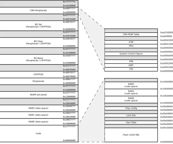
3.11 Memory Map
The EFM32PG12 memory map is shown in the figures below. RAM and flash sizes are for the largest memory configuration.
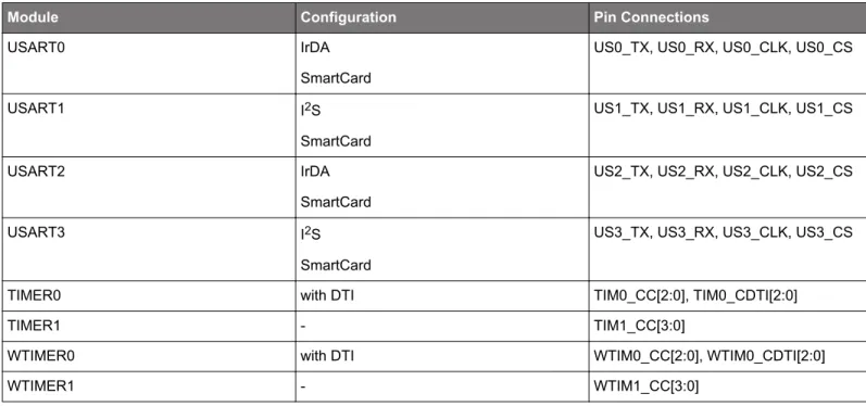
3.12 Configuration Summary
The features of the EFM32PG12 are a subset of the feature set described in the device reference manual. The table below describes device specific implementation of the features. Remaining modules support full configuration.
Table 3.2. Configuration Summary
Module Configuration Pin Connections
USART0 IrDA
SmartCard
US0_TX, US0_RX, US0_CLK, US0_CS
USART1 I2S
SmartCard
US1_TX, US1_RX, US1_CLK, US1_CS
USART2 IrDA
SmartCard
US2_TX, US2_RX, US2_CLK, US2_CS
USART3 I2S
SmartCard
US3_TX, US3_RX, US3_CLK, US3_CS
TIMER0 with DTI TIM0_CC[2:0], TIM0_CDTI[2:0]
TIMER1 - TIM1_CC[3:0]
WTIMER0 with DTI WTIM0_CC[2:0], WTIM0_CDTI[2:0]
4. Electrical Specifications
4.1 Electrical Characteristics
All electrical parameters in all tables are specified under the following conditions, unless stated otherwise:
• Typical values are based on TAMB=25 °C and VDD= 3.3 V, by production test and/or technology characterization.
• Minimum and maximum values represent the worst conditions across supply voltage, process variation, and operating temperature, unless stated otherwise.
Refer to 4.1.2.1 General Operating Conditions for more details about operational supply and temperature limits.
4.1.1 Absolute Maximum Ratings
Stresses above those listed below may cause permanent damage to the device. This is a stress rating only and functional operation of the devices at those or any other conditions above those indicated in the operation listings of this specification is not implied. Exposure to maximum rating conditions for extended periods may affect device reliability. For more information on the available quality and relia-bility data, see the Quality and Reliarelia-bility Monitor Report at http://www.silabs.com/support/quality/pages/default.aspx.
Table 4.1. Absolute Maximum Ratings
Parameter Symbol Test Condition Min Typ Max Unit
Storage temperature range TSTG -50 — 150 °C
Voltage on any supply pin VDDMAX -0.3 — 3.8 V
Voltage ramp rate on any supply pin
VDDRAMPMAX — — 1 V / µs
DC voltage on any GPIO pin VDIGPIN 5V tolerant GPIO pins123 -0.3 — Min of 5.25
and IOVDD +2
V
Standard GPIO pins -0.3 — IOVDD+0.3 V
Voltage on HFXO pins VHFXOPIN -0.3 — 1.4 V
Total current into VDD power lines
IVDDMAX Source — — 200 mA
Total current into VSS ground lines
IVSSMAX Sink — — 200 mA
Current per I/O pin IIOMAX Sink — — 50 mA
Source — — 50 mA
Current for all I/O pins IIOALLMAX Sink — — 200 mA
Source — — 200 mA
Junction temperature TJ -G grade devices -40 — 105 °C
-I grade devices -40 — 125 °C
Note:
1. When a GPIO pin is routed to the analog module through the APORT, the maximum voltage = IOVDD.
2. Valid for IOVDD in valid operating range or when IOVDD is undriven (high-Z). If IOVDD is connected to a low-impedance source below the valid operating range (e.g. IOVDD shorted to VSS), the pin voltage maximum is IOVDD + 0.3 V, to avoid exceeding the maximum IO current specifications.
3. To operate above the IOVDD supply rail, over-voltage tolerance must be enabled according to the GPIO_Px_OVTDIS register. Pins with over-voltage tolerance disabled have the same limits as Standard GPIO.
4.1.2 Operating Conditions
When assigning supply sources, the following requirements must be observed: • VREGVDD must be greater than or equal to AVDD, DVDD and all IOVDD supplies. • VREGVDD = AVDD
• DVDD ≤ AVDD • IOVDD ≤ AVDD
4.1.2.1 General Operating Conditions
Table 4.2. General Operating Conditions
Parameter Symbol Test Condition Min Typ Max Unit
Operating ambient tempera-ture range6
TA -G temperature grade -40 25 85 °C
-I temperature grade -40 25 125 °C
AVDD supply voltage2 VAVDD 1.8 3.3 3.8 V
VREGVDD operating supply voltage21
VVREGVDD DCDC in regulation 2.4 3.3 3.8 V
DCDC in bypass, 50mA load 1.8 3.3 3.8 V DCDC not in use. DVDD
external-ly shorted to VREGVDD
1.8 3.3 3.8 V
VREGVDD current IVREGVDD DCDC in bypass, T ≤ 85 °C — — 200 mA
DCDC in bypass, T > 85 °C — — 100 mA DVDD operating supply
volt-age
VDVDD 1.62 — VVREGVDD V
IOVDD operating supply volt-age
VIOVDD All IOVDD pins5 1.62 — VVREGVDD V
DECOUPLE output capaci-tor34
CDECOUPLE 0.75 1.0 2.75 µF
Difference between AVDD and VREGVDD, ABS(AVDD-VREGVDD)2
dVDD — — 0.1 V
HFCORECLK frequency fCORE VSCALE2, MODE = WS1 — — 40 MHz
VSCALE0, MODE = WS0 — — 20 MHz
HFCLK frequency fHFCLK VSCALE2 — — 40 MHz
VSCALE0 — — 20 MHz
Note:
1. The minimum voltage required in bypass mode is calculated using RBYP from the DCDC specification table. Requirements for
other loads can be calculated as VDVDD_min+ILOAD * RBYP_max.
2. VREGVDD must be tied to AVDD. Both VREGVDD and AVDD minimum voltages must be satisfied for the part to operate. 3. The system designer should consult the characteristic specs of the capacitor used on DECOUPLE to ensure its capacitance
val-ue stays within the specified bounds across temperature and DC bias.
4. VSCALE0 to VSCALE2 voltage change transitions occur at a rate of 10 mV / usec for approximately 20 usec. During this transi-tion, peak currents will be dependent on the value of the DECOUPLE output capacitor, from 35 mA (with a 1 µF capacitor) to 70 mA (with a 2.7 µF capacitor).
5. When the CSEN peripheral is used with chopping enabled (CSEN_CTRL_CHOPEN = ENABLE), IOVDD must be equal to AVDD. 6. The maximum limit on TA may be lower due to device self-heating, which depends on the power dissipation of the specific
appli-cation. TA (max) = TJ (max) - (THETAJA x PowerDissipation). Refer to the Absolute Maximum Ratings table and the Thermal
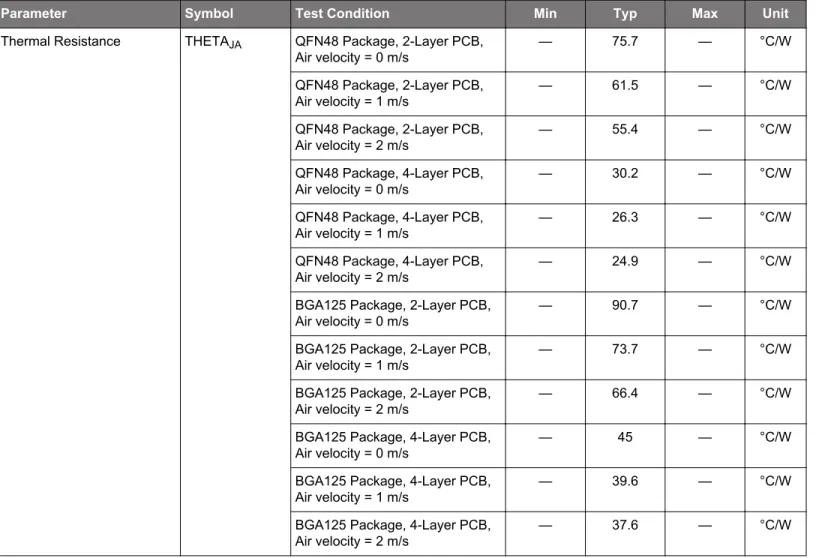
4.1.3 Thermal Characteristics
Table 4.3. Thermal Characteristics
Parameter Symbol Test Condition Min Typ Max Unit
Thermal Resistance THETAJA QFN48 Package, 2-Layer PCB, Air velocity = 0 m/s — 75.7 — °C/W QFN48 Package, 2-Layer PCB, Air velocity = 1 m/s — 61.5 — °C/W QFN48 Package, 2-Layer PCB, Air velocity = 2 m/s — 55.4 — °C/W QFN48 Package, 4-Layer PCB, Air velocity = 0 m/s — 30.2 — °C/W QFN48 Package, 4-Layer PCB, Air velocity = 1 m/s — 26.3 — °C/W QFN48 Package, 4-Layer PCB, Air velocity = 2 m/s — 24.9 — °C/W
BGA125 Package, 2-Layer PCB, Air velocity = 0 m/s
— 90.7 — °C/W
BGA125 Package, 2-Layer PCB, Air velocity = 1 m/s
— 73.7 — °C/W
BGA125 Package, 2-Layer PCB, Air velocity = 2 m/s
— 66.4 — °C/W
BGA125 Package, 4-Layer PCB, Air velocity = 0 m/s
— 45 — °C/W
BGA125 Package, 4-Layer PCB, Air velocity = 1 m/s
— 39.6 — °C/W
BGA125 Package, 4-Layer PCB, Air velocity = 2 m/s
4.1.4 DC-DC Converter
Test conditions: L_DCDC=4.7 µH (Murata LQH3NPN4R7MM0L), C_DCDC=4.7 µF (Samsung CL10B475KQ8NQNC), V_DCDC_I=3.3 V, V_DCDC_O=1.8 V, I_DCDC_LOAD=50 mA, Heavy Drive configuration, F_DCDC_LN=7 MHz, unless otherwise indicated.
Table 4.4. DC-DC Converter
Parameter Symbol Test Condition Min Typ Max Unit
Input voltage range VDCDC_I Bypass mode, IDCDC_LOAD = 50
mA
1.8 — VVREGVDD_
MAX
V
Low noise (LN) mode, 1.8 V out-put, IDCDC_LOAD = 100 mA, or
Low power (LP) mode, 1.8 V out-put, IDCDC_LOAD = 10 mA
2.4 — VVREGVDD_
MAX
V
Low noise (LN) mode, 1.8 V out-put, IDCDC_LOAD = 200 mA
2.6 — VVREGVDD_
MAX
V
Output voltage programma-ble range1
VDCDC_O 1.8 — VVREGVDD V
Regulation DC accuracy ACCDC Low Noise (LN) mode, 1.8 V tar-get output
1.7 — 1.9 V
Regulation window4 WINREG Low Power (LP) mode,
LPCMPBIASEMxx3 = 0, 1.8 V
tar-get output, IDCDC_LOAD ≤ 75 µA
1.63 — 2.2 V
Low Power (LP) mode,
LPCMPBIASEMxx3 = 3, 1.8 V
tar-get output, IDCDC_LOAD ≤ 10 mA
1.63 — 2.1 V
Steady-state output ripple VR — 3 — mVpp
Output voltage under/over-shoot
VOV CCM Mode (LNFORCECCM3 =
1), Load changes between 0 mA and 100 mA
— 25 60 mV
DCM Mode (LNFORCECCM3 =
0), Load changes between 0 mA and 10 mA
— 45 90 mV
Overshoot during LP to LN CCM/DCM mode transitions com-pared to DC level in LN mode
— 200 — mV
Undershoot during BYP/LP to LN CCM (LNFORCECCM3 = 1) mode
transitions compared to DC level in LN mode
— 40 — mV
Undershoot during BYP/LP to LN DCM (LNFORCECCM3 = 0) mode
transitions compared to DC level in LN mode
— 100 — mV
DC line regulation VREG Input changes between
VVREGVDD_MAX and 2.4 V
— 0.1 — %
DC load regulation IREG Load changes between 0 mA and
100 mA in CCM mode
Parameter Symbol Test Condition Min Typ Max Unit
Max load current ILOAD_MAX Low noise (LN) mode, Heavy
Drive2, T ≤ 85 °C
— — 200 mA
Low noise (LN) mode, Heavy Drive2, T > 85 °C
— — 100 mA
Low noise (LN) mode, Medium Drive2
— — 100 mA
Low noise (LN) mode, Light Drive2
— — 50 mA
Low power (LP) mode, LPCMPBIASEMxx3 = 0
— — 75 µA
Low power (LP) mode, LPCMPBIASEMxx3 = 3
— — 10 mA
DCDC nominal output ca-pacitor5
CDCDC 25% tolerance 1 4.7 4.7 µF
DCDC nominal output induc-tor
LDCDC 20% tolerance 4.7 4.7 4.7 µH
Resistance in Bypass mode RBYP — 1.2 2.5 Ω
Note:
1. Due to internal dropout, the DC-DC output will never be able to reach its input voltage, VVREGVDD.
2. Drive levels are defined by configuration of the PFETCNT and NFETCNT registers. Light Drive: PFETCNT=NFETCNT=3; Medi-um Drive: PFETCNT=NFETCNT=7; Heavy Drive: PFETCNT=NFETCNT=15.
3. LPCMPBIASEMxx refers to either LPCMPBIASEM234H in the EMU_DCDCMISCCTRL register or LPCMPBIASEM01 in the EMU_DCDCLOEM01CFG register, depending on the energy mode.
4. LP mode controller is a hysteretic controller that maintains the output voltage within the specified limits.
5. Output voltage under/over-shoot and regulation are specified with CDCDC 4.7 µF. Different settings for DCDCLNCOMPCTRL
4.1.5 Current Consumption
4.1.5.1 Current Consumption 3.3 V without DC-DC Converter
Unless otherwise indicated, typical conditions are: VREGVDD = AVDD = DVDD = 3.3 V. T = 25 °C. DCDC is off. Minimum and maxi-mum values in this table represent the worst conditions across supply voltage and process variation at T = 25 °C.
Table 4.5. Current Consumption 3.3 V without DC-DC Converter
Parameter Symbol Test Condition Min Typ Max Unit
Current consumption in EM0 mode with all peripherals dis-abled
IACTIVE 38.4 MHz crystal, CPU running
while loop from flash1
— 126 — µA/MHz
38 MHz HFRCO, CPU running Prime from flash
— 99 — µA/MHz
38 MHz HFRCO, CPU running while loop from flash
— 99 105 µA/MHz
38 MHz HFRCO, CPU running CoreMark from flash
— 124 — µA/MHz
26 MHz HFRCO, CPU running while loop from flash
— 102 108 µA/MHz
1 MHz HFRCO, CPU running while loop from flash
— 280 435 µA/MHz
Current consumption in EM0 mode with all peripherals dis-abled and voltage scaling enabled
IACTIVE_VS 19 MHz HFRCO, CPU running
while loop from flash
— 88 — µA/MHz
1 MHz HFRCO, CPU running while loop from flash
— 234 — µA/MHz
Current consumption in EM1 mode with all peripherals dis-abled
IEM1 38.4 MHz crystal1 — 76 — µA/MHz
38 MHz HFRCO — 50 54 µA/MHz
26 MHz HFRCO — 52 58 µA/MHz
1 MHz HFRCO — 230 400 µA/MHz
Current consumption in EM1 mode with all peripherals dis-abled and voltage scaling enabled
IEM1_VS 19 MHz HFRCO — 47 — µA/MHz
1 MHz HFRCO — 193 — µA/MHz
Current consumption in EM2 mode, with voltage scaling enabled
IEM2_VS Full 256 kB RAM retention and
RTCC running from LFXO
— 2.9 — µA
Full 256 kB RAM retention and RTCC running from LFRCO
— 3.2 — µA
16 kB (1 bank) RAM retention and RTCC running from LFRCO2
— 2.1 3.5 µA
Current consumption in EM3 mode, with voltage scaling enabled
IEM3_VS Full 256 kB RAM retention and
CRYOTIMER running from ULFR-CO
— 2.56 4.8 µA
Current consumption in EM4H mode, with voltage scaling enabled
IEM4H_VS 128 byte RAM retention, RTCC
running from LFXO
— 1.0 — µA
128 byte RAM retention, CRYO-TIMER running from ULFRCO
Parameter Symbol Test Condition Min Typ Max Unit
Current consumption in EM4S mode
IEM4S No RAM retention, no RTCC — 0.04 0.1 µA
Note:
1. CMU_HFXOCTRL_LOWPOWER=1.
4.1.5.2 Current Consumption 3.3 V using DC-DC Converter
Unless otherwise indicated, typical conditions are: VREGVDD = AVDD = IOVDD = 3.3 V, DVDD = 1.8 V DC-DC output. T = 25 °C. Minimum and maximum values in this table represent the worst conditions across supply voltage and process variation at T = 25 °C.
Table 4.6. Current Consumption 3.3 V using DC-DC Converter
Parameter Symbol Test Condition Min Typ Max Unit
Current consumption in EM0 mode with all peripherals dis-abled, DCDC in Low Noise DCM mode2
IACTIVE_DCM 38.4 MHz crystal, CPU running
while loop from flash4
— 86 — µA/MHz
38 MHz HFRCO, CPU running Prime from flash
— 70 — µA/MHz
38 MHz HFRCO, CPU running while loop from flash
— 70 — µA/MHz
38 MHz HFRCO, CPU running CoreMark from flash
— 85 — µA/MHz
26 MHz HFRCO, CPU running while loop from flash
— 77 — µA/MHz
1 MHz HFRCO, CPU running while loop from flash
— 636 — µA/MHz
Current consumption in EM0 mode with all peripherals dis-abled, DCDC in Low Noise CCM mode1
IACTIVE_CCM 38.4 MHz crystal, CPU running
while loop from flash4
— 96 — µA/MHz
38 MHz HFRCO, CPU running Prime from flash
— 81 — µA/MHz
38 MHz HFRCO, CPU running while loop from flash
— 82 — µA/MHz
38 MHz HFRCO, CPU running CoreMark from flash
— 95 — µA/MHz
26 MHz HFRCO, CPU running while loop from flash
— 95 — µA/MHz
1 MHz HFRCO, CPU running while loop from flash
— 1155 — µA/MHz
Current consumption in EM0 mode with all peripherals dis-abled, DCDC in LP mode3
IACTIVE_LPM 38.4 MHz crystal, CPU running
while loop from flash4
— 80 — µA/MHz
38 MHz HFRCO, CPU running Prime from flash
— 64 — µA/MHz
38 MHz HFRCO, CPU running while loop from flash
— 64 — µA/MHz
38 MHz HFRCO, CPU running CoreMark from flash
— 79 — µA/MHz
26 MHz HFRCO, CPU running while loop from flash
— 66 — µA/MHz
1 MHz HFRCO, CPU running while loop from flash
— 224 — µA/MHz
Current consumption in EM0 mode with all peripherals dis-abled and voltage scaling enabled, DCDC in Low
IACTIVE_CCM_VS 19 MHz HFRCO, CPU running
while loop from flash
— 101 — µA/MHz
Parameter Symbol Test Condition Min Typ Max Unit
Current consumption in EM0 mode with all peripherals dis-abled and voltage scaling enabled, DCDC in LP mode3
IACTIVE_LPM_VS 19 MHz HFRCO, CPU running
while loop from flash
— 58 — µA/MHz
1 MHz HFRCO, CPU running while loop from flash
— 196 — µA/MHz
Current consumption in EM1 mode with all peripherals dis-abled, DCDC in Low Noise DCM mode2
IEM1_DCM 38.4 MHz crystal4 — 56 — µA/MHz
38 MHz HFRCO — 41 — µA/MHz
26 MHz HFRCO — 48 — µA/MHz
1 MHz HFRCO — 610 — µA/MHz
Current consumption in EM1 mode with all peripherals dis-abled, DCDC in Low Power mode3
IEM1_LPM 38.4 MHz crystal4 — 49 — µA/MHz
38 MHz HFRCO — 33 — µA/MHz
26 MHz HFRCO — 35 — µA/MHz
1 MHz HFRCO — 194 — µA/MHz
Current consumption in EM1 mode with all peripherals dis-abled and voltage scaling enabled, DCDC in Low Noise DCM mode2
IEM1_DCM_VS 19 MHz HFRCO — 52 — µA/MHz
1 MHz HFRCO — 587 — µA/MHz
Current consumption in EM1 mode with all peripherals dis-abled and voltage scaling enabled. DCDC in LP mode3
IEM1_LPM_VS 19 MHz HFRCO — 32 — µA/MHz
1 MHz HFRCO — 170 — µA/MHz
Current consumption in EM2 mode, with voltage scaling enabled, DCDC in LP mode3
IEM2_VS Full 256 kB RAM retention and
RTCC running from LFXO
— 2.1 — µA
Full 256 kB RAM retention and RTCC running from LFRCO
— 2.2 — µA
16 kB (1 bank) RAM retention and RTCC running from LFRCO5
— 1.5 — µA
Current consumption in EM3 mode, with voltage scaling enabled
IEM3_VS Full 256 kB RAM retention and
CRYOTIMER running from ULFR-CO
— 1.81 — µA
Current consumption in EM4H mode, with voltage scaling enabled
IEM4H_VS 128 byte RAM retention, RTCC
running from LFXO
— 0.69 — µA
128 byte RAM retention, CRYO-TIMER running from ULFRCO
— 0.39 — µA
128 byte RAM retention, no RTCC — 0.39 — µA Current consumption in
EM4S mode
IEM4S No RAM retention, no RTCC — 0.06 — µA
Note:
1. DCDC Low Noise CCM Mode = Light Drive (PFETCNT=NFETCNT=3), F=6.4 MHz (RCOBAND=4), ANASW=DVDD. 2. DCDC Low Noise DCM Mode = Light Drive (PFETCNT=NFETCNT=3), F=3.0 MHz (RCOBAND=0), ANASW=DVDD. 3. DCDC Low Power Mode = Medium Drive (PFETCNT=NFETCNT=7), LPOSCDIV=1, LPCMPBIASEM234H=0,
LPCLIMILIM-4.1.5.3 Current Consumption 1.8 V without DC-DC Converter
Unless otherwise indicated, typical conditions are: VREGVDD = AVDD = DVDD = 1.8 V. T = 25 °C. DCDC is off. Minimum and maxi-mum values in this table represent the worst conditions across supply voltage and process variation at T = 25 °C.
Table 4.7. Current Consumption 1.8 V without DC-DC Converter
Parameter Symbol Test Condition Min Typ Max Unit
Current consumption in EM0 mode with all peripherals dis-abled
IACTIVE 38.4 MHz crystal, CPU running
while loop from flash1
— 126 — µA/MHz
38 MHz HFRCO, CPU running Prime from flash
— 99 — µA/MHz
38 MHz HFRCO, CPU running while loop from flash
— 99 — µA/MHz
38 MHz HFRCO, CPU running CoreMark from flash
— 124 — µA/MHz
26 MHz HFRCO, CPU running while loop from flash
— 102 — µA/MHz
1 MHz HFRCO, CPU running while loop from flash
— 277 — µA/MHz
Current consumption in EM0 mode with all peripherals dis-abled and voltage scaling enabled
IACTIVE_VS 19 MHz HFRCO, CPU running
while loop from flash
— 87 — µA/MHz
1 MHz HFRCO, CPU running while loop from flash
— 231 — µA/MHz
Current consumption in EM1 mode with all peripherals dis-abled
IEM1 38.4 MHz crystal1 — 76 — µA/MHz
38 MHz HFRCO — 50 — µA/MHz
26 MHz HFRCO — 52 — µA/MHz
1 MHz HFRCO — 227 — µA/MHz
Current consumption in EM1 mode with all peripherals dis-abled and voltage scaling enabled
IEM1_VS 19 MHz HFRCO — 47 — µA/MHz
1 MHz HFRCO — 190 — µA/MHz
Current consumption in EM2 mode, with voltage scaling enabled
IEM2_VS Full 256 kB RAM retention and RTCC running from LFXO
— 2.8 — µA
Full 256 kB RAM retention and RTCC running from LFRCO
— 3.0 — µA
16 kB (1 bank) RAM retention and RTCC running from LFRCO2
— 1.9 — µA
Current consumption in EM3 mode, with voltage scaling enabled
IEM3_VS Full 256 kB RAM retention and CRYOTIMER running from ULFR-CO
— 2.47 — µA
Current consumption in EM4H mode, with voltage scaling enabled
IEM4H_VS 128 byte RAM retention, RTCC
running from LFXO
— 0.91 — µA
128 byte RAM retention, CRYO-TIMER running from ULFRCO
— 0.35 — µA
Parameter Symbol Test Condition Min Typ Max Unit
Note:
1. CMU_HFXOCTRL_LOWPOWER=1.
2. CMU_LFRCOCTRL_ENVREF = 1, CMU_LFRCOCTRL_VREFUPDATE = 1
4.1.6 Wake Up Times
Table 4.8. Wake Up Times
Parameter Symbol Test Condition Min Typ Max Unit
Wakeup time from EM1 tEM1_WU — 3 — AHB
Clocks Wake up from EM2 tEM2_WU Code execution from flash — 10.1 — µs
Code execution from RAM — 3.2 — µs Wake up from EM3 tEM3_WU Code execution from flash — 10.1 — µs
Code execution from RAM — 3.2 — µs Wake up from EM4H1 tEM4H_WU Executing from flash — 80 — µs
Wake up from EM4S1 tEM4S_WU Executing from flash — 291 — µs
Time from release of reset source to first instruction ex-ecution
tRESET Soft Pin Reset released — 43 — µs
Any other reset released — 350 — µs Power mode scaling time tSCALE VSCALE0 to VSCALE2, HFCLK =
19 MHz42 — 31.8 — µs VSCALE2 to VSCALE0, HFCLK = 19 MHz3 — 4.3 — µs Note:
1. Time from wakeup request until first instruction is executed. Wakeup results in device reset.
2. VSCALE0 to VSCALE2 voltage change transitions occur at a rate of 10 mV/µs for approximately 20 µs. During this transition, peak currents will be dependent on the value of the DECOUPLE output capacitor, from 35 mA (with a 1 µF capacitor) to 70 mA (with a 2.7 µF capacitor).
3. Scaling down from VSCALE2 to VSCALE0 requires approximately 2.8 µs + 29 HFCLKs. 4. Scaling up from VSCALE0 to VSCALE2 requires approximately 30.3 µs + 28 HFCLKs.
4.1.7 Brown Out Detector (BOD)
Table 4.9. Brown Out Detector (BOD)
Parameter Symbol Test Condition Min Typ Max Unit
DVDD BOD threshold VDVDDBOD DVDD rising — — 1.62 V
DVDD falling (EM0/EM1) 1.35 — — V
DVDD falling (EM2/EM3) 1.3 — — V
DVDD BOD hysteresis VDVDDBOD_HYST — 18 — mV
DVDD BOD response time tDVDDBOD_DELAY Supply drops at 0.1V/µs rate — 2.4 — µs
AVDD BOD threshold VAVDDBOD AVDD rising — — 1.8 V
AVDD falling (EM0/EM1) 1.62 — — V
AVDD falling (EM2/EM3) 1.53 — — V
AVDD BOD hysteresis VAVDDBOD_HYST — 20 — mV
AVDD BOD response time tAVDDBOD_DELAY Supply drops at 0.1V/µs rate — 2.4 — µs
EM4 BOD threshold VEM4DBOD AVDD rising — — 1.7 V
AVDD falling 1.45 — — V
EM4 BOD hysteresis VEM4BOD_HYST — 25 — mV
4.1.8 Oscillators
4.1.8.1 Low-Frequency Crystal Oscillator (LFXO)
Table 4.10. Low-Frequency Crystal Oscillator (LFXO)
Parameter Symbol Test Condition Min Typ Max Unit
Crystal frequency fLFXO — 32.768 — kHz
Supported crystal equivalent series resistance (ESR)
ESRLFXO — — 70 kΩ
Supported range of crystal load capacitance 1
CLFXO_CL 6 — 18 pF
On-chip tuning cap range 2 CLFXO_T On each of LFXTAL_N and
LFXTAL_P pins
8 — 40 pF
On-chip tuning cap step size SSLFXO — 0.25 — pF
Current consumption after startup 3
ILFXO ESR = 70 kOhm, CL = 7 pF,
GAIN4 = 2, AGC4 = 1
— 273 — nA
Start- up time tLFXO ESR = 70 kOhm, CL = 7 pF,
GAIN4 = 2
— 308 — ms
Note:
1. Total load capacitance as seen by the crystal.
2. The effective load capacitance seen by the crystal will be CLFXO_T /2. This is because each XTAL pin has a tuning cap and the
two caps will be seen in series by the crystal.
3. Block is supplied by AVDD if ANASW = 0, or DVDD if ANASW=1 in EMU_PWRCTRL register. 4. In CMU_LFXOCTRL register.
4.1.8.2 High-Frequency Crystal Oscillator (HFXO)
Table 4.11. High-Frequency Crystal Oscillator (HFXO)
Parameter Symbol Test Condition Min Typ Max Unit
Crystal frequency fHFXO 38 38.4 40 MHz
Supported crystal equivalent series resistance (ESR)
ESRHFXO_38M4 Crystal frequency 38.4 MHz — — 60 Ω
Supported range of crystal load capacitance 1
CHFXO_CL 6 — 12 pF
On-chip tuning cap range 2 CHFXO_T On each of HFXTAL_N and
HFXTAL_P pins
9 20 25 pF
On-chip tuning capacitance step
SSHFXO — 0.04 — pF
Startup time tHFXO 38.4 MHz, ESR = 50 Ohm, CL =
10 pF
— 300 — µs
Frequency tolerance for the crystal
FTHFXO 38.4 MHz, ESR = 50 Ohm, CL =
10 pF
-40 — 40 ppm
Note:
1. Total load capacitance as seen by the crystal.
2. The effective load capacitance seen by the crystal will be CHFXO_T /2. This is because each XTAL pin has a tuning cap and the two caps will be seen in series by the crystal.
4.1.8.3 Low-Frequency RC Oscillator (LFRCO)
Table 4.12. Low-Frequency RC Oscillator (LFRCO)
Parameter Symbol Test Condition Min Typ Max Unit
Oscillation frequency fLFRCO ENVREF2 = 1 31.3 32.768 33.6 kHz
ENVREF2 = 1, T > 85 °C 31.6 32.768 36.8 kHz
ENVREF2 = 0 31.3 32.768 33.4 kHz
ENVREF2 = 0, T > 85 °C 30.0 32.768 33.4 kHz
Startup time tLFRCO — 500 — µs
Current consumption 1 ILFRCO ENVREF = 1 in
CMU_LFRCOCTRL — 370 — nA ENVREF = 0 in CMU_LFRCOCTRL — 520 — nA Note:
1. Block is supplied by AVDD if ANASW = 0, or DVDD if ANASW=1 in EMU_PWRCTRL register. 2. In CMU_LFRCOCTRL register.
4.1.8.4 High-Frequency RC Oscillator (HFRCO)
Table 4.13. High-Frequency RC Oscillator (HFRCO)
Parameter Symbol Test Condition Min Typ Max Unit
Frequency accuracy fHFRCO_ACC At production calibrated
frequen-cies, across supply voltage and temperature
-2.5 — 2.5 %
Start-up time tHFRCO fHFRCO ≥ 19 MHz — 300 — ns
4 < fHFRCO < 19 MHz — 1 — µs
fHFRCO ≤ 4 MHz — 2.5 — µs
Maximum DPLL lock time1 tDPLL_LOCK fREF = 32.768 kHz, fHFRCO =
39.98 MHz, N = 1219, M = 0
— 183 — µs
Current consumption on all supplies
IHFRCO fHFRCO = 38 MHz — 244 265 µA
fHFRCO = 32 MHz — 204 222 µA fHFRCO = 26 MHz — 173 188 µA fHFRCO = 19 MHz — 143 156 µA fHFRCO = 16 MHz — 123 136 µA fHFRCO = 13 MHz — 110 124 µA fHFRCO = 7 MHz — 85 94 µA fHFRCO = 4 MHz — 32 37 µA fHFRCO = 2 MHz — 28 34 µA fHFRCO = 1 MHz — 26 31 µA
fHFRCO = 40 MHz, DPLL enabled — 423 470 µA
fHFRCO = 32 MHz, DPLL enabled — 338 375 µA
fHFRCO = 16 MHz, DPLL enabled — 192 220 µA
fHFRCO = 4 MHz, DPLL enabled — 51 75 µA
fHFRCO = 1 MHz, DPLL enabled — 36 50 µA
Coarse trim step size (% of period)
SSHFRCO_COARS E
— 0.8 — %
Fine trim step size (% of pe-riod)
SSHFRCO_FINE — 0.1 — %
Period jitter PJHFRCO — 0.2 — % RMS
Note:
4.1.8.5 Auxiliary High-Frequency RC Oscillator (AUXHFRCO)
Table 4.14. Auxiliary High-Frequency RC Oscillator (AUXHFRCO)
Parameter Symbol Test Condition Min Typ Max Unit
Frequency accuracy fAUXHFRCO_ACC At production calibrated
frequen-cies, across supply voltage and temperature
-3 — 3 %
Start-up time tAUXHFRCO fAUXHFRCO ≥ 19 MHz — 400 — ns
4 < fAUXHFRCO < 19 MHz — 1.4 — µs
fAUXHFRCO ≤ 4 MHz — 2.5 — µs
Current consumption on all supplies
IAUXHFRCO fAUXHFRCO = 38 MHz — 193 213 µA
fAUXHFRCO = 32 MHz — 157 175 µA fAUXHFRCO = 26 MHz — 135 151 µA fAUXHFRCO = 19 MHz — 108 122 µA fAUXHFRCO = 16 MHz — 100 113 µA fAUXHFRCO = 13 MHz — 77 88 µA fAUXHFRCO = 7 MHz — 53 63 µA fAUXHFRCO = 4 MHz — 29 36 µA fAUXHFRCO = 2 MHz — 28 34 µA fAUXHFRCO = 1 MHz — 27 31 µA
Coarse trim step size (% of period)
SS AUXHFR-CO_COARSE
— 0.8 — %
Fine trim step size (% of pe-riod)
SS AUXHFR-CO_FINE
— 0.1 — %
Period jitter PJAUXHFRCO — 0.2 — % RMS
4.1.8.6 Ultra-low Frequency RC Oscillator (ULFRCO)
Table 4.15. Ultra-low Frequency RC Oscillator (ULFRCO)
Parameter Symbol Test Condition Min Typ Max Unit
4.1.9 Flash Memory Characteristics5
Table 4.16. Flash Memory Characteristics5
Parameter Symbol Test Condition Min Typ Max Unit
Flash erase cycles before failure
ECFLASH 10000 — — cycles
Flash data retention RETFLASH T ≤ 85 °C 10 — — years
T ≤ 125 °C 10 — — years
Word (32-bit) programming time
tW_PROG Burst write, 128 words, average time per word
20 24.4 30 µs
Single word 60 68.4 80 µs
Page erase time4 tPERASE 20 26.4 35 ms
Mass erase time1 tMERASE 20 26.5 35 ms
Device erase time23 tDERASE T ≤ 85 °C — 82 100 ms
T ≤ 125 °C — 82 110 ms
Erase current6 IERASE Page Erase — — 1.6 mA
Write current6 IWRITE — — 3.8 mA
Supply voltage during flash erase and write
VFLASH 1.62 — 3.6 V
Note:
1. Mass erase is issued by the CPU and erases all flash.
2. Device erase is issued over the AAP interface and erases all flash, SRAM, the Lock Bit (LB) page, and the User data page Lock Word (ULW).
3. From setting the DEVICEERASE bit in AAP_CMD to 1 until the ERASEBUSY bit in AAP_STATUS is cleared to 0. Internal setup and hold times for flash control signals are included.
4. From setting the ERASEPAGE bit in MSC_WRITECMD to 1 until the BUSY bit in MSC_STATUS is cleared to 0. Internal setup and hold times for flash control signals are included.
5. Flash data retention information is published in the Quarterly Quality and Reliability Report. 6. Measured at 25 °C.
4.1.10 General-Purpose I/O (GPIO)
Table 4.17. General-Purpose I/O (GPIO)
Parameter Symbol Test Condition Min Typ Max Unit
Input low voltage VIL GPIO pins — — IOVDD*0.3 V
Input high voltage VIH GPIO pins IOVDD*0.7 — — V
Output high voltage relative to IOVDD
VOH Sourcing 3 mA, IOVDD ≥ 3 V,
DRIVESTRENGTH1 = WEAK
IOVDD*0.8 — — V
Sourcing 1.2 mA, IOVDD ≥ 1.62 V,
DRIVESTRENGTH1 = WEAK
IOVDD*0.6 — — V
Sourcing 20 mA, IOVDD ≥ 3 V, DRIVESTRENGTH1 = STRONG
IOVDD*0.8 — — V
Sourcing 8 mA, IOVDD ≥ 1.62 V, DRIVESTRENGTH1 = STRONG
IOVDD*0.6 — — V
Output low voltage relative to IOVDD
VOL Sinking 3 mA, IOVDD ≥ 3 V, DRIVESTRENGTH1 = WEAK
— — IOVDD*0.2 V
Sinking 1.2 mA, IOVDD ≥ 1.62 V, DRIVESTRENGTH1 = WEAK
— — IOVDD*0.4 V
Sinking 20 mA, IOVDD ≥ 3 V, DRIVESTRENGTH1 = STRONG
— — IOVDD*0.2 V
Sinking 8 mA, IOVDD ≥ 1.62 V, DRIVESTRENGTH1 = STRONG
— — IOVDD*0.4 V
Input leakage current IIOLEAK All GPIO except LFXO pins, GPIO
≤ IOVDD, T ≤ 85 °C
— 0.1 30 nA
LFXO Pins, GPIO ≤ IOVDD, T ≤ 85 °C
— 0.1 50 nA
All GPIO except LFXO pins, GPIO ≤ IOVDD, T > 85 °C
— — 110 nA
LFXO Pins, GPIO ≤ IOVDD, T > 85 °C
— — 250 nA
Input leakage current on 5VTOL pads above IOVDD
I5VTOLLEAK IOVDD < GPIO ≤ IOVDD + 2 V — 3.3 15 µA
I/O pin pull-up/pull-down re-sistor
RPUD 30 40 65 kΩ
Pulse width of pulses re-moved by the glitch suppres-sion filter
Parameter Symbol Test Condition Min Typ Max Unit
Output fall time, From 70% to 30% of VIO tIOOF CL = 50 pF, DRIVESTRENGTH1 = STRONG, SLEWRATE1 = 0x6 — 1.8 — ns CL = 50 pF, DRIVESTRENGTH1 = WEAK, SLEWRATE1 = 0x6 — 4.5 — ns
Output rise time, From 30% to 70% of VIO tIOOR CL = 50 pF, DRIVESTRENGTH1 = STRONG, SLEWRATE = 0x61 — 2.2 — ns CL = 50 pF, DRIVESTRENGTH1 = WEAK, SLEWRATE1 = 0x6 — 7.4 — ns Note: 1. In GPIO_Pn_CTRL register.
4.1.11 Voltage Monitor (VMON)
Table 4.18. Voltage Monitor (VMON)
Parameter Symbol Test Condition Min Typ Max Unit
Supply current (including I_SENSE)
IVMON In EM0 or EM1, 1 supply
moni-tored, T ≤ 85 °C
— 6.3 10 µA
In EM0 or EM1, 1 supply moni-tored, T > 85 °C
— — 14 µA
In EM0 or EM1, 4 supplies moni-tored, T ≤ 85 °C
— 12.5 17 µA
In EM0 or EM1, 4 supplies moni-tored, T > 85 °C
— — 21 µA
In EM2, EM3 or EM4, 1 supply monitored and above threshold
— 62 — nA
In EM2, EM3 or EM4, 1 supply monitored and below threshold
— 62 — nA
In EM2, EM3 or EM4, 4 supplies monitored and all above threshold
— 99 — nA
In EM2, EM3 or EM4, 4 supplies monitored and all below threshold
— 99 — nA
Loading of monitored supply ISENSE In EM0 or EM1 — 2 — µA
In EM2, EM3 or EM4 — 2 — nA
Threshold range VVMON_RANGE 1.62 — 3.4 V
Threshold step size NVMON_STESP Coarse — 200 — mV
Fine — 20 — mV
Response time tVMON_RES Supply drops at 1V/µs rate — 460 — ns