研 究 成 果 報 告 書
────────────────────────────────────――――
半導体量子構造系におけるキャリアー量子捕獲および離脱機構
────────────────────────────────────――――
課題番号 16360157
平成16年度〜平成18年度科学研究費補助金
(基盤研究(B)) 研究成果報告書
平成19年6月
研究代表者 藤 原 賢 三
九州工業大学工学部教授
<はしがき>
この報告書は、平成16年度から3年間にわたり実施したInGaN量子井戸 構造を有する発光ダイオードの発光効率に関する研究をまとめたもので ある。エレクトロルミネッセンス効率の注入電流と温度依存性、フォトルミ ネッセンス発光効率の外部バイアスと温度依存性、光励起波長依存性、光励 起強度依存性についての結果を総合的にまとめたものである。
研 究 組 織
研究代表者 : 藤 原 賢 三 (九州工業大学工学部教授)
研究分担者 : 佐 竹 昭 泰 (九州工業大学工学部助手)
(研究協力者 : 副島 健一 )
(研究協力者 : 稲田 隆之 )
(研究協力者 : 相澤 秀幸 )
(研究協力者 : 尾辻 直樹 )
(研究協力者 : 加藤 博文 )
(研究協力者 : 山根 勇一 )
交付決定額(配分額) (金額単位:円)
直接経費 間 接 経
費
合 計 平成16年度 4,500,000 0 4,500,000 平成17年度 1,400,000 0 1,400,000 平成18年度 1,100,000 0 1,100,000 総 計 7,000,000 0 7,000,000
研 究 発 表
(1)学会誌等
1. N. Otsuji, Y. Takahashi, A. Satake, K. Fujiwara, J. K. Shue, U. Jahn, H. Kostial, and H. T. Grahn,
“ Impact of the forward bias on the radiative recombination efficiency in blue (In,Ga)N/GaN quantum-well diodes with an electron reservoir layer”,
Proceedings of 13th International Semiconducting and Insulating Materials Conference (Bejin, China, September 20-24, 2004), pp. 276-280 (2004).
(平成16年9月20日)
2. A. Satake, K. Soejima, H. Aizawa, and K. Fujiwara,
“Carrier capture and escape processes in (In,Ga)N single-quantum-well diode under forward bias condition by photoluminescence spectroscopy”,
Phys. Stat. Sol.(c) 3[6], pp. 2203-2206 (2006).
(平成18年5月12日)
3. H. Aizawa, K. Soejima, A. Hori, A. Satake, and K. Fujiwara,
“Interplay of external and internal field effects on radiative recombination efficiency in InGaN quantum well diodes”,
Phys. Stat. Sol. (c)3[3], pp. 589-593 (2006).
(平成18年2月22日)
4.N. Otsuji, K. Fujiwara, and J. K. Sheu,
“Electroluminescence efficiency of blue InGaN/GaN quantum well diodes with and without an n-InGaN electron reservoir layer”,
J. Appl. Phys. 100[11], pp113105-1-7 (2006).
(平成18年12月5日)
5. A. Hori, D. Yasunaga, K. Fujiwara,
“Impact of forward bias on electroluminescence efficiency in blue and green InGaN quantum well diodes: A comparative study”,
Thin Solid Films, Vol. 515, pp. 4480-4483 (2007).
(平成18年8月28日)
6. T. Inoue, K. Fujiwara, and J. K. Sheu,
“Hole escape processes deterimental to photoluminescence efficiency in a blue InGaN multiple-quantum-well diode under reverse bias conditions”,
Appl. Phys. Lett. 90[16], pp. 161109-1-3 (2007).
(平成19年4月17日)
7. T. Inada, A. Satake, and K. Fujiwara,
“Significance of vertical carrier capture for electroluminescence efficiency in InGaN multiple-quantum well diodes”,
Phys. Stat. Sol. (c) 4[7], 2768-2771 (2007).
(平成19年5月31日)
8 .T. Inoue,
K. Fujiwara, and J. K. Sheu,
“External Field Effects on Photoluminescence Properties of Blue InGaN Quantum-Well Diodes”,
Proceedings of the 2006 Conference on Optoelectronic and Microelectronic Materials and Devices, to be published by the IEEE Press.
(平成19年 印刷中)
(2)口頭発表
国際会議発表
1. A. Hori, D. Yasunaga and K. Fujiwara,
“Effects of Forward Bias Conditions on Electroluminescence Efficiency in Blue and Green InGaN Single-Quantum-Well Diodes”,
16th International Conference on Indium Phosphide and Related Materials, (Kagoshima, Japan, May 31-June 4 (2004) (P1-25)).
2. N. Otsuji, Y. Takahashi, A. Satake, K. Fujiwara, J. K. Shue, U. Jahn, H. Kostial, and H. T. Grahn,
“Impact of the forward bias on the radiative recombination efficiency in blue (In,Ga)N/GaN quantum-well diodes with an electron reservoir layer”,
13th International Semiconducting and Insulating Materials Conference, (Bejin, China, September 20-24, 2004).
3. A. Hori, D. Yasunaga, and K. Fujiwara,
“Impact of the forward bias on electroluminescence efficiency in blue and green InGaN quantum well diodes: a comparative study”,
International Conference on Materials for Advanced Technology, (Singapore, July 3-8, 2005 (J-4-P037)).
4. N. Otsuji, H. Katou, A. Satake, K. Fujiwara, J. K. Shue, U. Jahn, H. Kostial, and H.
T. Grahn,
“Spectral evidence for escape of injected carriers in blue (In,Ga)N/GaN quantum-well diodes under high forward-bias conditions”,
International Conference on Nitride Semiconductors,
(Bremen, Germany, August 28-September 2, 2005 (Th-P-144 Late News)).
5. A. Satake, K. Soejima, H. Aizawa, and K. Fujiwara,
“Carrier capture and escape processes in (In,Ga)N single-quantum-well diode under forward bias condition by photoluminescence spectroscopy”,
International Conference on Nitride Semiconductors, (Bremen, Germany, August 28-September 2, 2005 (Th-P-101)).
6. H. Aizawa, K. Soejima, A. Hori, A. Satake, and K. Fujiwara,
“Interplay of external and internal field effects on radiative recombination efficiency in InGaN quantum well diodes”,
International Symposium on Compound Semiconductors,
(Rust near Freiburg, Germany, September 18-22, 2005 (Th1.3)).
7. K. Fujiwara,
“Impact of Forward bias on the electroluminescence efficiency in InGaN quantum well diodes”,
Japan-German-Spain Symposium on Semiconductors, (Berlin , Germany, March 8-9, 2006 (invited talk)).
8. T. Inada, A. Satake, and K. Fujiwara,
“Significance of Vertical Carrier Capture for Electroluminescence Efficiency in InGaN Multiple-Quantum-Well Diodes”,
The International Workshop on Nitrides in 2006
((IWN2006), October 22-27, 2006, Kyoto, Japan (TuP2-28)).
9. T. Inoue,
K. Fujiwara, and J. K. Sheu,
“External Field Effects on Photoluminescence Properties of Blue InGaN Quantum-Well Diodes”,
The 2006 Conference on Optoelectronic and Microelectronic Materials and Devices ((COMMAD ʼ06), Perth, Australia, December 6-8, 2006 (WO-A1)).
10. K. Fujiwara, H. Katou, T. Inoue,
and J. K. Sheu,
“Luminescence efficiency in blue InGaN quantum-well diodes: impact of forward bias conditions”,
3
rdInternational Conference on Advanced Materials and Nanotechnology ((AMN-3), February 11-16, 2007, Wellington, New Zealand (Poster)).
国内学会発表
11. 尾辻直樹、高橋慶彦、加藤博文、佐竹昭泰、藤原賢三、
“キャリアー溜層付加による青色InGaN量子井戸発光ダイオードの発光効率の増大”、
第9回九州薄膜表面研究会(九州工業大学、2004年6月19日).
12. 尾辻直樹、高橋慶彦、加藤博文、佐竹昭泰、藤原賢三、
“電子溜層付加による青色InGaN量子井戸発光ダイオードの発光効率の増大”、
応用物理学会九州支部講演会、28Ca-9、2004年11月28日(琉球大学).
13. 佐竹昭泰、尾辻直樹、加藤博文、藤原賢三、
“電子溜層付InGaN量子井戸発光ダイオードにおけるフォトルミネッセンスのバイアス依存 性”、
応用物理学会九州支部講演会、28Ca-10、2004年11月28日(琉球大学).
14. 加藤博文、尾辻直樹、高橋慶彦、佐竹昭泰、藤原賢三、
“電子溜層付き青色 InGaN 量子井戸発光ダイオードの発光特性”、
第52回応用物理学関係連合講演会、31a-V-30、2005 年 3 月 31 日(埼玉大学).
15. 山根勇一、堀口雅司、加藤博文、佐竹昭泰、藤原賢三、
“ホールトンネリング注入型青色InGaN発光ダイオードの発光特性”、
応用物理学会九州支部講演会、1Ba-3、2005年11月26日(福岡工業大学).
16. 加藤博文、井上貴雄、山根勇一、佐竹昭泰、藤原賢三、
“電子溜層付き青色InGaN量子井戸発光ダイオードのフォトルミネッセンス特性”、
応用物理学会九州支部講演会、1Ba-4、2005年11月26日(福岡工業大学).
17. 副島健一、稲田隆之、佐竹昭泰、藤原賢三、
“緑色及び青色InGaN単一量子井戸発光ダイオードのフォトルミネッセンス電界効果”、
応用物理学会九州支部講演会、2Aa-10、2005年11月27日(福岡工業大学).
18. 稲田隆之、副島健一、佐竹昭泰、藤原賢三、
“青色・緑色多重量子井戸発光ダイオードのエレクトロルミネッセンス強度の温度依存性”、
応用物理学会九州支部講演会、aAa-12、2005年11月27日(福岡工業大学).
19. 稲田隆之、佐竹昭泰、藤原賢三、
“InGaN多重量子井戸ダイオードの垂直キャリア捕獲とエレクトロルミネセンス効率”、
応用物理学会学術講演会、31a-RE10/III、2006年8月31日(立命館大学、草津キャンパス).
20. 佐竹昭泰、副島健一、相澤秀幸、藤原賢三、
“InGaN SQW LED におけるフォトルミネッセンスの電界依存性−励起波長による影響−”、
応用物理学会学術講演会、1a-RE11/III、2006 年 9 月 1 日(立命館大学、草津キャンパス).
21. 稲田隆之、堀口雅司、自見弘幸、佐竹昭泰、藤原賢三、
“青色・緑色InGaN多重量子井戸発光ダイオードの発光効率”、
応用物理学会九州支部講演会、25Ca-7、2006年11月25日(大分大学).
22. 堀口雅司、山根勇一、稲田隆之、自見弘幸、佐竹昭泰、藤原賢三、
“InGaN発光ダイオードの電流電圧特性の温度依存性”、
応用物理学会九州支部講演会、25Cp-1、2006年11月25日(大分大学).
23. 井上貴雄、佐竹昭泰、加藤博文、藤原賢三、
“青色InGaN発光ダイオードのフォトルミネッセンス電界効果”、
応用物理学会九州支部講演会、25Cp-2、2006年11月25日(大分大学).
24. 佐竹昭泰、副島健一、相澤秀幸、藤原賢三、
“InGaN 単一量子井戸発光ダイオードの電界印加フォトルミネッセンス強度の温度依存性”、
応用物理学会九州支部講演会、25Cp-6、2006年11月25日(大分大学).
25. 山根勇一、井上貴雄、堀口雅司、佐竹昭泰、藤原賢三、
“電子溜め層付き青色InGaN発光ダイオードの発光効率”、
応用物理学会九州支部講演会、25Cp-7、2006年11月25日(大分大学).
研究成果報告書の概要
InGaN系量子井戸発光ダイオードは、エピタキシャル成長層と基板間の格子不整合が大きいために 10
10cm
-2程度の非常に多くの貫通転位が存在し欠陥密度が大きいにもかかわらず、発光効率が非常に高 い。この高効率発光の機構を探るために、エレクトロルミネッセンス(EL)及びフォトルミネッセン ス(PL)発光強度の外部電界効果を、(イ)EL発光効率の格子温度依存性及び(ロ)注入電流依存性、
(ハ)PL発光効率の温度依存性及び(ニ)励起光波長依存性(直接励起と間接励起)、励起光強度依 存性について、研究を実施した。その結果、以下の成果が得られた。
(1) エレクトロルミネッセンス(EL)発光効率の温度及び注入電流依存性の研究
青色及び緑色InGaN単一量子井戸発光ダイオードのEL発光強度の温度依存性(20-300K)から、特に、
100K以下の低温で見られたEL強度の減少は、注入電流レベルが低いとき、また、In組成の異なる青色 と緑色素子間で著しく変化する、即ち、注入キャリアーの捕獲効率の変化が重要であることを明らか にした。
(2) 電子溜層付加によるInGaN量子井戸ダイオードのEL発光効率と量子捕獲改善効果の研究 N型電子溜層の有無による青色多重量子井戸発光ダイオードのEL発光効率の温度依存性(20-300K)か ら、電子溜層の付加により、発光効率はすべての温度範囲、注入電流レベルで強められることを明ら かにした。また、高注入電流と低注入電流時の比較から、主EL発光バンド効率の低温に於ける減少割 合の変化及び短波長サテライトバンド発光効率の相関は、順バイアス電圧下でのキャリアー捕獲の違 いにより起こ得ることを明らかにした。
(3) 緑色発光ダイドードのPL発光効率の外部電界効果とキャリアー捕獲及び離脱過程の研究 緑色InGaN単一量子井戸ダイオードのPL発光強度の外部電界効果を、直接励起及び間接励起条件下で 測定した。直接励起条件では+2V以上の順バイアス電圧で、また、逆バイアス条件下で、PL強度の減 少が起こること、即ち、順バイアス電圧下でのキャリアー離脱による発光効率の減少が起こることを 直接的に検証した。さらに、間接励起下では、+2-3V程度の順バイアス下で発光効率が増大し、+3.25V 以上の順バイアス印加により著しく発光効率が減少する、即ち、障壁層から発光層へのキャリアー捕 獲が発光効率に重要な役割を果たしていることを明らかにした。
(4) 緑色InGaN単一量子井戸発光ダイオードの発光効率と外部電界効果の研究
緑色InGaN単一量子井戸ダイオードのEL発光効率の100K以下の低温に見られた減少は、高注入電流時 に顕著であるが、低注入電流時には起こらないこと、即ち、順バイアス電圧の大きさがキャリアーの 発光中心への捕獲に重要な役割を演じていることを、直接励起下でのPL発光強度のバイアス電圧依存 性との比較から明らかにした。
(5) 青色InGaN量子井戸発光ダイオードのPL発光効率と外部電界効果の研究
N型電子溜層付青色多重量子井戸発光ダイオードのPL発光効率外部電界効果の実験、特に、励起光強 度依存性の実験から、電子溜層と活性層のPL強度比較により、逆バイアス下でのPL発光の減少は光生 成した正孔の捕獲により律則されることを明らかにした。
CHAPTER 1
Impact of forward bias on the radiative recombination
efficiency in blue and green InGaN quantum well diodes
CHAPTER 2
Electroluminescence efficiency of blue InGaN/GaN quantum well
diodes with and without an n-InGaN electron reservoir layer
Electroluminescence efficiency of blue InGaN / GaN quantum-well diodes with and without an n-InGaN electron reservoir layer
N. Otsuji and K. Fujiwaraa兲
Department of Electrical Engineering, Kyushu Institute of Technology, Tobata, Kitakyushu 804-8550, Japan
J. K. Sheu
Institute of Electro-Optical Science and Engineering, National Cheng-Kung University, Tainan 701, Taiwan
共Received 4 July 2006; accepted 16 September 2006; published online 5 December 2006兲
The temperature dependence of the electroluminescence共EL兲
spectral intensity has been investigated in detail betweenT= 20 and 300 K at various injection current levels for a set of two blue InGaN / GaN multiple-quantum-well共MQW兲
light-emitting diodes共LEDs兲
with and without an additional n-doped In0.18Ga0.82N electron reservoir layer共ERL兲. The radiative recombination
efficiency of the main blue emission band共⬃480 nm兲
is found to be significantly improved at all temperature regions and current levels when the additional ERL is introduced. For high injection currentsIf, i.e., large forward bias voltagesVf, a quenching of the EL intensity is observed forT⬍100 K for both LED structures, accompanying appearance of short-wavelength satellite emissions around 380– 430 nm. Furthermore, the low-temperature intensity reduction of the main EL band is stronger for the LED without the ERL than with the ERL. For lowIf, i.e., smallVf, however, no quenching of the EL intensity is observed for both LEDs even below 100 K and the short-wavelength satellite emissions are significantly reduced. These results of the main blue emission and the short-wavelength satellite bands imply that the unusual evolution of the EL intensity with temperature and current is caused by variations of the actual potential field distribution due to both internal and external fields. They significantly influence the carrier capture efficiency by radiative recombination centers within the active MQW layer and the carrier escape out of the active regions into high-energy recombination centers responsible for the short-wavelength satellite emissions. ©2006 American Institute of Physics.
关DOI:
10.1063/1.2398690兴I. INTRODUCTION
Despite the great success of blue and green light- emitting diodes
共LEDs兲
based on InGaN quantum-well共QW兲
heterostructures, the origin of the very bright emission char- acteristics is still controversially discussed.1–10 A peculiar property of this material system is the observation of effi- cient luminescence at room temperature, although the den- sity of misfit dislocations can be as high as 1010cm−2due to the large lattice mismatch between the InGaN / GaN epitaxial layers and the sapphire substrate. Therefore, we expect the existence of a particular mechanism, which is responsible for the enhancement of the radiative efficiency in the presence of a high defect density. Previous studies of the temperature- dependent electroluminescence共EL兲
spectral intensity in single-QW共SQW兲
diodes7,8show that efficient capture pro- cesses of injected carriers by localized tail states within the SQW layer play an important role for the recombination ef- ficiency between T= 180 and 300 K. However, for T⬍100 K, an anomalous quenching of the EL intensity is ob- served, which we attribute to a reduction of the vertical car- rier capture rates.7We have also investigated the temperature dependence of the EL intensity for a specially designed blue
InGaN / GaN multiple-QW
共MQW兲
LED containing an addi- tionaln-doped InGaN electron reservoir layer共ERL兲.
11This LED exhibits a significant improvement of the radiative ef- ficiency in comparison with the LED without the ERL. In relation to the high luminescence efficiency under the pres- ence of the high defect density in InGaN MQWs, Hangleiter et al.12and Hitzelet al.13recently proposed that most of the defects in the active region can be decorated by the higher band gap materials thus blocking the carriers to be nonradia- tively extinguished, leading to the improved radiative recom- bination in spite of the existence of high defect density. This lateral carrier blocking mechanism against defect trapping within the active quantum-well layer is involved with the emissions at short-wavelength regions. Therefore, it is inter- esting to seek for whether the short-wavelength satellite emissions are correlated with the main EL band when the radiative recombination efficiency is significantly changed as a function of temperature and bias due to the changes of carrier capture efficiency by the radiative recombination cen- ters.In this paper, we report on a detailed investigation of the EL intensity of InGaN / GaN LEDs with and without the ERL as a function of temperature and injection current level to study how the carrier capture efficiency varies with bias con- ditions. By comparing the temperature-dependent EL charac-
a兲FAX:⫹81-93-884-0879; electronic mail: [email protected]
JOURNAL OF APPLIED PHYSICS100, 113105
共
2006兲
0021-8979/2006/100
共
11兲
/113105/7/$23.00 100, 113105-1 © 2006 American Institute of PhysicsDownloaded 11 Dec 2006 to 150.69.51.85. Redistribution subject to AIP license or copyright, see http://jap.aip.org/jap/copyright.jsp
teristics of the two MQW-LEDs for low and high injection currents over a wide spectral range, the enhanced EL effi- ciency observed in the MQW-LED with the ERL is attributed to an improved electron capture by radiative recombination centers. This capture is significantly influenced by the ap- plied forward bias conditions
共
external field effects兲
. Good correlation between the main EL efficiency and the short- wavelength satellite emission band is obtained.II. EXPERIMENT
A set of two InGaN / GaN MQW-LEDs without and with an additional n-doped In0.18Ga0.82N electron reservoir layer
共
ERL兲
, named LED I and LED II, respectively, were grown by metal-organic vapor-phase epitaxy.14A schematic layered structure of the LEDs is shown in Fig.1. The emission re- gion of the LEDs consists of a triple In0.3Ga0.7N QW with a nominal width of 2.5 nm separated by 6.5 nm GaN barriers.This MQW layer is clad by 4 m n-GaN and 30 nm p -Al0.15Ga0.85N layers. A 15-nm-thick n-doped
共⬃10
19cm−3兲
In0.18Ga0.82N ERL is located between then-GaN clad and the active MQW layer. A thickness of n-doped GaN barrier be- tween the ERL and the active layer is thinned to be 3 nm.The p-i-n diode is formed by forming metal contacts on 0.25m p-GaN cap layer and the n-GaN clad layer laterally.14 Thus, in this set of two diodes
共LED I and II兲,
only the addition of the ERL between the active MQW and the n-GaN barrier layers is different. EL spectra of the MQW-LEDs mounted on a Cu cold stage of a closed-cycle He cryostat were recorded for the dominating blue MQW emission band as well as for high-energy bands from other layers by conventional lock-in detection techniques at tem- peratures between 20 and 300 K as a function of the injected current between 1.0 and 50 mA.III. RESULTS AND DISCUSSION
The current-voltage
共I
f-Vf兲
characteristics of LEDs I and II have been measured betweenT= 20 and 300 K. Figure 2 shows representative If-Vfcurves at 20, 140, and 300 K. At 300 K, a typicalVfvalue forIf= 10 mA for LED II is 2.9 V, while for LED I the corresponding value of Vf is 3.6 V, so that a smallerVfis necessary to achieve the same value ofIffor LED II with the ERL than for LED I without the ERL.
That is, the forward bias voltage to get a certain current level is significantly reduced for LED II. This means that the stan-
dard Shockley recombination theory15 needs to be modified by the additional heterostructure configuration. When the lat- tice temperature is decreased to 20 K, theIf-Vf characteris- tics also change significantly, and the forward bias to obtain a current level increases substantially probably due to the reduced density of holes because of trapping by the deep Mg accepter level. That is, there are fewer holes in the p-type region at lower temperatures than at room temperature. At 20 K, the difference between the values of Vf for the two LEDs becomes even larger. When the temperature is de- creased from 300 to 20 K in Fig. 2, the forward bias to achieve a sufficient current level, say 10 mA, is increased by about 2 – 3 V in both LEDs. This increase of the forward bias with decreasing temperature is most probably due to the re- duced hole conductivity in thep-GaN andp-共Al, Ga兲N lay- ers at lower temperatures. In addition, we find a clear differ- ence in the slope of the logarithm ofIf as a function of Vf
between the two samples as well as between room and low temperatures
共not shown here兲. Further investigations are
necessary to fully understand the observed temperature de- pendence of theIf-Vf characteristics and the different behav- iors of the two LEDs. It should be noted, however, that the trapping of holes at 20 K due to the deep Mg accepter level共⬃170 meV兲
in p-GaN cannot explain all the observedFIG. 1.
共
Color online兲
Schematic layered structure of the InGaN / GaN MQW-LEDs without共
LED I兲
and with an additionaln-type In0.18Ga0.82N ERL共
LED II兲
.FIG. 2.If-Vfcurves at 20, 140, and 300 K of the InGaN / GaN MQW-LEDs without
共
LED I: open symbols兲
and with an additionaln-type In0.18Ga0.82N ERL共
LED II: full symbols兲
.113105-2 Otsuji, Fujiwara, and Sheu J. Appl. Phys.100, 113105
共
2006兲
Downloaded 11 Dec 2006 to 150.69.51.85. Redistribution subject to AIP license or copyright, see http://jap.aip.org/jap/copyright.jsp
changes between LED I and LED II, since the p-GaN and p-共Al, Ga兲N layers
共with hole concentrations of ⬃10
17cm−3兲
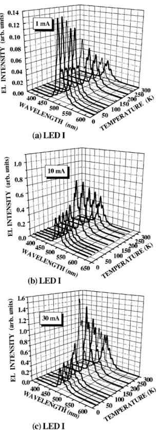
are nominally identical in both samples. Here, we would like to emphasize that the addition of a widen-In0.18Ga0.82N layer between then-GaN barrier and the MQW layer has a signifi- cant impact on theIf-Vfcharacteristics, i.e., it reducesVffor a particular value ofIf.Figure3shows EL spectra of LED I without the ERL as a function of temperature at three injection current levels:
共a兲
1.0 mA,
共b兲
10 mA, and共c兲
30 mA. The EL spectra exhibit intense emission around 480 nm with additional fine struc- tures due to Fabry-Pe´rot interference fringes. When the in- jection current level is low at 1.0 mA in Fig.3共
a兲
, the leading EL band exhibits the highest intensity at 20 K, and the EL peak intensity decreases as the temperature is increased. This decrease of the EL intensity with increasing the temperature is ascribed to an enhancement of nonradiative recombination processes, i.e., a reduction of the radiative recombination ef- ficiency. When the current level is increased, however, the temperature dependence of the EL intensity is drastically changed, as illustrated in Figs.3共
b兲
and3共
c兲
. A reduction of the EL intensity is clearly seen with decreasing the tempera- ture below 100 K after reaching the maximum EL intensity around 140 K. At 30 mA关Fig.
3共c兲兴the EL intensity reduc- tion is significant at 20 K and the difference in EL intensity between 140 and 20 K becomes larger than at 10 mA关Fig.
3共b兲兴. The similar temperature dependence of EL spectra is plotted in Fig.4for LED II with the ERL. At 1.0 mA
关shown
in Fig.4共a兲兴the EL intensity observed as a function of tem- perature shows the similar behavior as the LED I, that is, the reduction of EL intensity with increasing the temperature.The maximum of the spectrally integrated EL intensity is reached at 20 K in Fig.4共a兲. This enhancement of the radia- tive recombination efficiency around 20 K is commonly ob- served for both types of LEDs, which is similar to the pho- toluminescence
共PL兲
efficiency enhancement observed at low temperatures due to the reduced nonradiative recombination.5,10 However, it is important to note that the absolute EL intensity for LED II becomes larger than that for LED I for all temperatures共
note the ordinate scale change兲
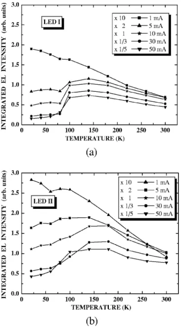
. When the injection current level is increased to 10 mA, the difference in EL temperature dependence between LED I and LED II becomes even larger. That is, the EL reduction with decreasing temperature is strongly suppressed at 10 and 30 mA in Figs.4共b兲and4共c兲in comparison with Figs. 3共b兲 and3共c兲. The LED II with the ERL always shows a stronger EL intensity than LED I without the ERL, in agreement with our previous results.11,14In order to further investigate the origin of the reduced EL efficiency at lower temperatures and higher injection lev- els, we have also evaluated the spectrally integrated EL in- tensity divided by the current, that is, the EL external quan- tum efficiency as a function of temperature for different injection current levels. Figures5
共
a兲
and5共
b兲
show the inte- grated EL intensity as a function of temperature at various current levels from 1.0 to 50 mA共
normalized to the case of 10 mA兲 for LED I and LED II, respectively. For If= 1.0 mA, the EL efficiency exhibits its highest value at 20 K, which monotonously decreases with increasing tem- perature in both cases. When the injection level is increased to 10 mA, the EL efficiency per injection current decreases in comparison with the case ofIf= 1.0 mA. Note that the EL efficiency effectively decreases with increasing current level up to 50 mA for both LEDs. Therefore, we conclude that the reduction of Vf for LED II in comparison with LED I
共cf.
Fig.2兲plays an important role in the enhancement of the EL efficiency at 20 K. We emphasize that the EL efficiency per injected carrier is highest at the lowest current of 1.0 mA at
FIG. 3. Temperature-dependent EL spectra of LED I without an additional ERL for
共
a兲
If= 1 mA,共
b兲
10 mA, and共
c兲
30 mA.113105-3 Otsuji, Fujiwara, and Sheu J. Appl. Phys.100, 113105
共
2006兲
Downloaded 11 Dec 2006 to 150.69.51.85. Redistribution subject to AIP license or copyright, see http://jap.aip.org/jap/copyright.jsp
all temperatures in Fig. 5 for both of the diodes. It appears that the carriers are effectively captured by active centers in the MQW under the application of lower forward biases.
But, applying higher forward biases, they are rather trans- ferred to nonradiative recombination centers as a result of escape from the MQW region, thus reducing the EL effi- ciency. This is because the carriers can escape out of the well region due to the internal field effects, since the junction field
direction is opposite to the internal field. We also note that the higher field existing in the well under the higher forward bias decreases the radiative recombination rate due to the quantum-confined Stark effect, which also causes the re- duced EL intensity.
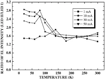
In Fig.5, it is noted that the difference in the EL inten- sity between the two LEDs becomes even larger at 20 K for If= 30 mA than forIf= 1.0 mA
共cf. also Figs.
3 and4兲. The difference of a factor of about 2 is seen between the EL intensities in Figs.3共a兲and4共a兲as well as in Figs.3共c兲and 4共c兲. ForIf= 1.0 mA the ratio of the EL intensities of LED II to LED I is approximately temperature independent. But it strongly increases with decreasing temperature for If= 30 mA. In order to demonstrate this difference more clearly, the ratio of the integrated EL intensity of LED II to LED I is plotted in Fig.6forIf= 1.0, 10, 30, and 50 mA as a function of temperature. Note that the EL intensity of LED II is always stronger than that of LED I, irrespective of tem- perature and current level. Furthermore, the enhancement of
FIG. 4. Temperature-dependent EL spectra of LED II with an additional ERL for
共
a兲
If= 1 mA,共
b兲
10 mA, and共
c兲
30 mA.FIG. 5. Temperature dependence of integrated EL intensity of
共
a兲
LED I without and共
b兲
LED II with an additional ERL forIf= 1, 10, 30, and 50 mA.113105-4 Otsuji, Fujiwara, and Sheu J. Appl. Phys.100, 113105
共
2006兲
Downloaded 11 Dec 2006 to 150.69.51.85. Redistribution subject to AIP license or copyright, see http://jap.aip.org/jap/copyright.jsp
the EL efficiency with decreasing temperature
共around
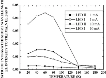
20– 80 K兲 is significant for LED II over LED I. The im- provement of the EL efficiency for LED II with the ERL is, in fact, remarkable, indicating the importance of the carrier escape processes from radiative recombination centers in the InGaN MQW layer under the presence of higher forward biases.In order to verify the carrier escape from the active MQW layer to the barrier regions, we have measured short- wavelength EL spectra around 360– 450 nm below the lead- ing blue
共⬃480 nm兲
EL band including the spectral regions of the barrier materials and the ERL. The results are shown in Fig.7for LED I关共a兲
and共b兲兴
and for LED II关共c兲
and共d兲兴
at low共1.0 mA兲
and high共10 mA兲
currents, respectively. In Fig. 7共a兲 for LED I and at 1.0 mA, more than 100 times weaker emissions are seen at short-wavelength regions关peaked around 420 nm 共2.95 eV兲兴
than the main blue共
⬃480 nm兲
band. The intensity of the satellite EL band mo- notonously increases with decreasing temperature, while the main EL band shows appreciable increases in intensity at 1.0 mA. Therefore, the results in Fig. 7共
a兲
are explained by the fact that the EL efficiency is basically determined by the internal quantum efficiency due to the reduced nonradiative recombination processes. When the current is increased to 10 mA in Fig. 7共b兲, however, the EL intensity of satellite emissions drastically increases by almost one order of the magnitude relative to the main band and more rapidly in- creases when decreasing temperatures below 100 K. The EL efficiency of the main blue band thus decreases at 20 K when the current increases, as indicated in Fig.5共a兲. That is, the main EL peak intensity decreases at temperatures below 140 K when the current is higher than 10 mA. On the other hand, as shown in Figs.7共
c兲
and7共
d兲
, the short-wavelength satellite band of LED II is found to be much weaker than that of LED I. Enhancement of the satellite emission with in- creasing the current to 10 mA is not so significant in Fig.7共d兲, indicating the improved carrier capture efficiency by the active region. This result is consistent with the improved radiative recombination efficiency in Figs.4共b兲and4共c兲, es-
pecially at lower temperatures. But it is worth to note that the satellite EL emission also rapidly increases below 100 K in Fig.7共d兲in a similar way as in Fig.7共b兲.
Figure 8 shows the satellite EL emission efficiency by
FIG. 6. Temperature dependence of ratio of integrated EL intensity
共
LED II/LED I兲
forIf= 1, 10, 30, and 50 mA.FIG. 7. Short-wavelength EL spectra of
关共
a兲
and共
b兲兴
LED I without and关共
c兲
and共
d兲兴
LED II with an additional ERL forIf= 1 and 10 mA, respectively.113105-5 Otsuji, Fujiwara, and Sheu J. Appl. Phys.100, 113105
共
2006兲
Downloaded 11 Dec 2006 to 150.69.51.85. Redistribution subject to AIP license or copyright, see http://jap.aip.org/jap/copyright.jsp
plotting ratio of the integrated short-wavelength EL intensity divided by the integrated main EL intensity for LED I and II at low
共1.0 mA兲
and high共10 mA兲
current levels as a func- tion of temperature. For the injection current of 10 mA the short-wavelength emission efficiency of LED I is, in fact, increased at lower temperatures共below 100 K兲, indicating a
reduction in the carrier capture rates by the MQW layer.11 For LED II this increase of the satellite emission at 10 mA is significantly reduced and therefore the EL efficiency is im- proved due to the increased carrier capture efficiency. We note in Figs.7and8that, as the temperature goes down to 20 from 60 K, the short-wavelength satellite EL intensity slightly decreases. This is especially true for the injection current of 10 mA, while the main EL band is decreasing. We attribute these simultaneous intensity decreases of the main and satellite EL bands at 20 K to the reduction of the carrier injection efficiency from the clad layers into the active/barrier regions due to the decreased carrier mobility
共most
probably due to the decreased hole mobility兲.In Fig.7the broad satellite EL band at short wavelengths around 370– 430 nm
共2.88– 3.35 eV兲
is definitely enhanced under the higher forward bias conditions. It is important and interesting to inquire what the origin of this broad EL band is and whether the satellite band is related to the short- wavelength PL band共3.0– 3.3 eV兲
observed by Hitzelet al.13 for the high-band-gap material, effective as the carrier block- ing layer against defect trapping. In our analysis the EL ef- ficiency of the satellite band, which sensitively changes with bias and temperature, is simply used as a measure for the carrier escape out of the active regions in the MQW layer.Since our observation shows that the satellite EL band is significantly suppressed by the addition of ERL, electrons injected from the n-type ERL are more efficiently captured into the active regions under the forward bias conditions.
This is because the band gap energy of the ERL material
共estimated to be ⬃3.06 eV by a sharp PL peak observed兲
is lower than the GaN barriers共3.5 eV兲, so that the carrier
overshoot is suppressed, thus enhancing the main blue EL band. One possibility for those overshooting electrons with-out the ERL is that they are to be captured in thep-GaN cap layer. Thus, the satellite emissions might be due to the donor- acceptor
共D-A兲
pairs in the p-GaN cap layer. However, the broad共the bandwidth ⬃0.47 eV兲
satellite emission band and the large Stokes shifts共0.15– 0.62 eV兲
observed are not con- sistent with the D-A recombination, as pointed out by Yang et al.10As a matter of fact, the satellite EL band is enhanced with increasing the forward bias and without the ERL. So, this emission band should not be related to the InGaN alloy fluctuations in the well layers共because the alloy effects are
the same for both samples兲, but rather related to the barrier GaN layers. It is interesting to point out that the thinner sidewall quantum well as observed by transmission electron microscope12 may also contribute to the stronger radiative recombination at the short-wavelength EL band. The ob- served broad linewidth for the satellite EL band may be ex- plained if we take the quantum-confined Stark effect共QCSE兲
due to the internal field under the forward bias into account.However, more work is obviously necessary to elucidate the detailed carrier escape mechanisms under the forward bias conditions. Nevertheless, it is clear that the carrier capture by the MQW active regions is significantly improved by the additional ERL and by reducing the forward bias voltage, thus enhancing the EL efficiency by current injection.
IV. CONCLUSION
The EL spectral intensity of the main blue and the short- wavelength satellite bands has been investigated as a func- tion of temperature and injection current for a set of two In0.3Ga0.7N / GaN triple-quantum-well light-emitting diodes without and with an additional n-doped In0.18Ga0.82N elec- tron reservoir layer. We find that the temperature variation of the EL efficiency critically depends on the injection current level and the presence of the additional ERL. For low current levels and thus small forward bias voltages, EL quenching does not occur below 100 K due to efficient carrier capture, as evidenced by the reduced satellite EL band. However, for high injection current levels and thus large forward bias volt- ages, the EL quenching persists below 100 K, and its tem- perature variation is more pronounced in the LED without the ERL. This unique temperature dependence of the EL intensity variation at different injection levels originates from the difference in the forward bias voltage. Appearance of the short-wavelength satellite band when the main blue emission band is reduced is consistent with the EL mecha- nism by Hangleiteret al.12 and Hitzedet al.13These results imply that the unusual evolution of the EL efficiency with current level and temperature can be caused by variations of the potential field distribution due to both internal and exter- nal fields, which significantly influence the carrier capture efficiency within the MQW active layer.
ACKNOWLEDGMENTS
The authors would like to thank H. Kostial, U. Jahn, and H. T. Grahn of Paul-Drude Institute for Solid State Electron- ics in Berlin, Germany for sample wiring and useful discus- sion. They also thank Y. Takahashi, H. Katou, and A. Satake for their experimental assistance. This work was supported in
FIG. 8. Temperature dependence of ratio of the integrated short-wavelength EL intensity to the main EL band of LED I without and LED II with an additional ERL forIf= 1 and 10 mA.
113105-6 Otsuji, Fujiwara, and Sheu J. Appl. Phys.100, 113105
共
2006兲
Downloaded 11 Dec 2006 to 150.69.51.85. Redistribution subject to AIP license or copyright, see http://jap.aip.org/jap/copyright.jsp
part by the Grant-in-Aid for Scientific Research from the Ministry of Education, Culture, Sport, Science, and Technol- ogy of Japan under the Contract No. 16360157.
1S. Nakamura and G. Fasol,The Blue Laser Diode
共
Springer-Verlag, Ber- lin, 1997兲
.2S. Nakamura, M. Senoh, N. Iwasa, S. Nagahama, T. Yamada, and T. Mu- kai, Jpn. J. Appl. Phys., Part 2 34, L1332
共
1995兲
.3T. Takeuchi, S. Sota, M. Katsuragawa, M. Komori, H. Takeuchi, H.
Amano, and I. Akasaki, Jpn. J. Appl. Phys., Part 2 36, L382
共
1997兲
.4T. Mukai, K. Takekawa, and S. Nakamura, Jpn. J. Appl. Phys., Part 2 37, L839
共
1998兲
.5Y. Narukawa, Y. Kawakami, S. Fujita, and S. Nakamura, Phys. Rev. B59, 10283
共
1999兲
.6K. P. O’Donnell, R. W. Martin, and P. G. Middleton, Phys. Rev. Lett. 82, 237
共1999兲.
7A. Hori, D. Yasunaga, A. Satake, and K. Fujiwara, Appl. Phys. Lett. 79, 3723
共
2001兲
; J. Appl. Phys. 93, 3152共
2003兲
.8A. Hori, D. Yasunaga, A. Satake, and K. Fujiwara, Phys. Status Solidi A 192, 44
共
2002兲
.9X. A. Cao, S. F. LeBoeuf, L. B. Rowland, C. H. Yan, and H. Liu, Appl.
Phys. Lett. 82, 3614
共
2003兲
.10C. L. Yanget al., J. Appl. Phys.98, 23703
共
2005兲
.11Y. Takahashi, A. Satake, K. Fujiwara, J. K. Sheu, U. Jahn, H. Kostial, and H. T. Grahn, Physica E
共
Amsterdam兲
21, 876共
2004兲
.12A. Hangleiter, F. Hitzel, C. Netzel, D. Fuhrmann, U. Rossow, G. Ade, and P. Hinze, Phys. Rev. Lett. 95, 127402
共
2005兲
.13F. Hitzel, G. Klewer, S. Lahmann, U. Rossow, and A. Hangleiter, Phys.
Rev. B 72, 081309R
共
2005兲
.14J. K. Sheu, G. C. Chi, and M. J. Jou, IEEE Photonics Technol. Lett. 13, 1164
共
2001兲
.15E. Fred Schubert, Light-Emitting Diodes
共
Cambridge University Press, Cambridge, UK, 2005兲
.113105-7 Otsuji, Fujiwara, and Sheu J. Appl. Phys.100, 113105
共
2006兲
Downloaded 11 Dec 2006 to 150.69.51.85. Redistribution subject to AIP license or copyright, see http://jap.aip.org/jap/copyright.jsp
CHAPTER 3
Carrier capture and escape processes in InGaN single quantum
well diode under forward bias condition by photoluminescence
spectroscopy
CHAPTER 4
Interplay of external and internal field effects on radiative
recombination efficiency in InGaN quantum well diodes
CHAPTER 5
External field effects on photoluminescence properties of
blue InGaN quantum well diodes
Hole escape processes detrimental to photoluminescence efficiency
in a blue InGaN multiple-quantum-well diode under reverse bias conditions
T. Inoue and K. Fujiwaraa兲
Kyushu Institute of Technology, Tobata, Kitakyushu 804-8550, Japan J. K. Sheu
Institute of Electro-Optical Science and Engineering, National Cheng-Kung University, Tainan, Taiwan 70101, Republic of China
共
Received 1 February 2007; accepted 16 March 2007; published online 17 April 2007兲
Photoluminescence
共PL兲
properties of a blue In0.3Ga0.7N multiple-quantum-well共MQW兲
diode with an additionaln+-doped In0.18Ga0.82N electron reservoir layer共ERL兲
have been investigated at 20 K as a function of reverse bias under indirect barrier excitation. A PL intensity ratio of MQW/ERL is observed to be significantly quenched by increasing the reverse field due to electron-hole separation and carrier escape, in spite of observed blueshifts, when the excitation power is decreased by two orders of magnitude. The PL intensity reduction suggests that the hole escape process plays an important role for determination of the PL efficiency under the reverse bias. © 2007 American Institute of Physics.关DOI:
10.1063/1.2723683兴Despite the realization of blue and green light-emitting diodes
共LEDs兲
based on InGaN / GaN quantum-well共QW兲
heterostructures,1,2 the origin of the very bright emission characteristics is still controversially discussed.3–8A peculiar property of this material system is the observation of effi- cient luminescence, although the density of misfit disloca- tions can be as high as 1010cm−2. Therefore, we expect the existence of a particularly important mechanism, which is responsible for the enhancement of the radiative efficiency in the presence of a very high defect density. Previously quan- tum confinement effects on the InGaN alloy well and effi- cient carrier capturing by the localized radiative recombina- tion centers have been claimed to be important for the origin of the high emission efficiency. Quite recently, importance of very efficient hole capture processes by localizing valence states associated with atomic condensates of In–N for radia- tive recombination efficiency is pointed out.9,10 Thus, all of the previous studies infer that carrier capture processes to- ward radiative recombination centers and prohibition of es- cape to nonradiative defective sites play an important role for the determination of the radiative recombination efficiency.3–13 In relation to assessment of the radiative re- combination efficiency, we have recently investigated the temperature dependence of the electroluminescence共EL兲
in- tensity for a specially designed blue InGaN / GaN multiple-QW共
MQW兲
-LED containing an additional n+-doped InGaN electron reservoir layer共ERL兲.
14,15 This LED exhibits a significant improvement of the EL efficiency, in particular, for lower temperatures, when a forward bias necessary to obtain a certain injection current is high due to the reduced hole conductivity.In this letter, photoluminescence
共PL兲
properties of the blue InGaN MQW-LED with ERL have been investigated with a special emphasis on external field effects on the ra- diative recombination processes. The existence of n+-type ERL below the active MQW layer allows us to monitor how the photogenerated carrier distribution across the active MQW region influences the PL efficiency by changing exci-tation power as a function of field strength. Observed PL intensity reduction induced by the reverse fields suggests im- portance of hole escape processes from the MQW for the determination of the PL efficiency.
An InGaN / GaN MQW-LED with an additional n+-doped In0.18Ga0.82N ERL was grown by metal-organic vapor-phase epitaxy.16The emission region of the LED con- sists of a triple In0.3Ga0.7N QW with a nominal width of 2.5 nm separated by 6.5 nm GaN barriers. Details of the MQW-LED heterostructure were described previously.15,16 PL spectra have been recorded over a wide spectral range as a function of forward and reverse bias voltages at 20 K with a lock-in detection technique, using a He–Cd laser at 325 nm for indirect photoexcitation at various excitation powers of 0.1– 10 mW
共power density of ⬃1 – 10
2W / cm2兲.
Figure 1共a兲shows PL spectra of the diode taken with a 10 mW laser power and at 4.25, 2.0, 0, and −3.0 V. When excited from the surface p-GaN cap layer, the MQW diode shows a main blue MQW emission band around 480 nm, which is strongly redshifted due to carrier localization from absorption band tails, as confirmed by photocurrent spectra
共
not shown兲
. In addition to the main blue emission band, a distinct PL band at 405 nm is observed only for the diode with ERL, but not for a similar MQW diode without it.Therefore, the PL band at 405 nm is identified as originating from the ERL located below the active MQW layer. A broad short-wavelength emission band is also observed around 380– 440 nm, the origin of which is not clear at present. A small but sharp PL band observed at 355 nm is ascribed to bound excitons in the GaN layers. A broad PL band due to yellow emissions around 575 nm is also observed, only when the GaN barriers are indirectly photoexcited. When the forward bias is decreased and the reverse bias is increased to
−3 V, the PL intensity of the main blue band is considerably decreased, accompanying blueshifts, while the emission in- tensity of then+-doped ERL remains the same without any peak shifts. These results indicate that the external field is applied to the MQW region only and that the quantum con- fined Stark effect results in the compensation of the internal
a兲Electronic mail: [email protected]
APPLIED PHYSICS LETTERS90, 161109
共
2007兲
0003-6951/2007/90
共
16兲
/161109/3/$23.00 90, 161109-1 © 2007 American Institute of Physics Downloaded 17 Apr 2007 to 150.69.51.85. Redistribution subject to AIP license or copyright, see http://apl.aip.org/apl/copyright.jsppiezofield, which is opposite to the p-n junction field direction.5,13
On the other hand, when the excitation power is de- creased by two orders of magnitude to 0.1 mW, two substan- tial differences appear in the PL spectra, as shown in Fig.1
共
b兲
. That is, a PL intensity ratio of MQW/ERL is ob- served to be drastically increased at a forward bias of 4.25 V共near the flatband condition兲
due to a decrease of photon penetration depth共relative decrease of the ERL emission兲
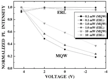
and preferential photoexcitation of the front MQW region near thep-type clad layer. Secondly, the MQW PL intensity is significantly quenched by increasing the reverse field due to field-induced electron-hole separation and resultant carrier escape, in spite of observed blueshifts. Figure2shows nor- malized, wavelength-integrated PL intensity for MQW and ERL as a function of applied reverse bias at excitation pow- ers of 0.1, 1.0, and 10 mW. It is clear that the PL intensity for MQW significantly decreases with increasing the reverse field and the reduction is stronger under the weak excitation power, while the ERL emission remains to be nearly con- stant. This field-induced PL intensity reduction dependent on the photoexcitation power suggests that the hole escape pro-cess plays an important role for determination of the blue PL efficiency under the reverse bias conditions, as discussed in the following.
The bias dependence of the PL spectra significantly changes by decreasing the excitation power and the PL in- tensity decreases very rapidly with increasing the reverse bias
共external field兲
under the weak excitation关see Fig.
1共b兲兴.Note that the PL intensity decreases to 18%, when the re- verse bias is increased to −3 from +4.25 V. We attribute these PL spectral variations with decrease of the excitation power to the decreased excitation depth. This hypothesis can be easily confirmed because of the existence of the ERL.
That is, then+-type ERL which is located below the active region is more weakly photoexcited by the weak photoexci- tation. We observe systematical decreases of the PL intensity for ERL relative to the main blue emission band, when the excitation power is decreased to 0.1 from 10 mW. But it is not surprising to find out that the ERL PL band does not show any discernible changes in intensity with bias at all excitation levels, since the ERL is heavily doped ton+type
共⬃
1019cm−3兲
. However, when the reverse bias is increased, the intensity of the main PL band around 480 nm certainly decreases more slowly under the intense excitation, in con- trast to the case of the weak excitation.These variations of the PL intensity quenching by the reverse bias
共
reverse field兲
at various excitation powers can be explained in the following ways. Figure3 illustrates the potential diagram of the MQW diode under the共a兲
weak and共b兲
intense excitation conditions. When the photon penetra- tion depth is shallow as in Fig. 3共a兲, the photogenerated electron-hole pairs are not uniform across the MQW layer and more carriers are excited in the front well layer near the p-type barrier. Therefore, the photogenerated holes can es- cape more easily from the active well layer, when the reverse field is increased, leading to the rapid decreases of the PL intensity. However, under the intense excitation关see Fig.
3共b兲兴 the MQW layer is rather uniformly excited and photoexcited carriers are generated deep into the bottom well layer. This is evidenced by the strong increase of the PL intensity for ERL. Therefore, the PL intensity of the main blue band results in slow decrease with increasing reverse bias, since holes generated in the bottom well near the ERLFIG. 1. PL spectra of a blue In0.3Ga0.7N MQW-LED with an additional n-type In0.18Ga0.82N electron reservoir layer
共
ERL兲
as a function of forward共
positive兲
and reverse共
negative兲
bias voltages at 20 K under共
a兲
intense共
10 mW power兲
and共
b兲
weak共
0.1 mW power兲
indirect excitations at a wavelength of 325 nm. Note that the main PL peak around 480 nm shows a moderate共
strong兲
intensity reduction in共
a兲 关
in共
b兲兴
with increasing the re- verse bias voltage, accompanying blueshifts, while the ERL emission at 405 nm does not change its intensity. A small line seen at 650 nm is due to the laser scattering.FIG. 2. Normalized, wavelength-integrated PL intensity for MQW and ERL bands as a function of reverse
共
negative兲
bias voltage at three different excitation powers of 0.1, 1.0, and 10 mW.161109-2 Inoue, Fujiwara, and Sheu Appl. Phys. Lett.90, 161109
共
2007兲
Downloaded 17 Apr 2007 to 150.69.51.85. Redistribution subject to AIP license or copyright, see http://apl.aip.org/apl/copyright.jsp