PAPER
Special Section on Analog Circuit Techniques and Related TopicsA Low-Power Current-Reuse LNA for 3D Ultrasound Beamformers
Yohei NAKAMURA†a), Shinya KAJIYAMA†,Members, Yutaka IGARASHI††,Nonmember, Takashi OSHIMA†, andTaizo YAMAWAKI†,Members
SUMMARY 3D ultrasound imagers require low-noise amplifier (LNA) with much lower power consumption and smaller chip area than conven- tional 2D imagers because of the huge amount of transducer channels.
This paper presents a low-power small-size LNA with a novel current- reuse circuitry for 3D ultrasound imaging systems. The proposed LNA is composed of a differential common source amplifier and a source-follower driver which share the current without using inductors. The LNA was fab- ricated in a 0.18-µm CMOS process with only 0.0056 mm2. The measured results show a gain of 21 dB and a bandwidth of 9 MHz. The proposed LNA achieves an average noise density of 11.3 nV/√
Hz, and the 2nd har- monic distortion below−40 dBc with 0.1-Vpp input. The supply current is 85µA with a 1.8-V power supply, which is competitive with conventional LNAs by finer CMOS process.
key words: amplifier, current-reuse, driver, ultrasound, LNA
1. Introduction
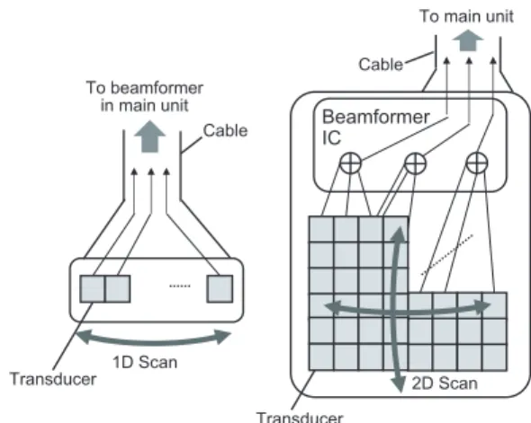
Ultrasound imaging systems are widely used for medical diagnosis. A 1D array probe is commonly used to obtain 2D images, but 3D imaging systems with 2D array probes have been used recently to minimize examination time and to make it easier to find a target[1]–[3]. In the conven- tional 1D probe, a received ultrasound signal is converted into an electrical signal at a transducer array in the handheld probe and usually transmitted to a main unit that has a beam- focusing function as shown in Fig. 1(a). However, for the 2D array probe, this function must be integrated in the probe as shown in Fig. 1(b) to avoid a too heavy transceiver cable to the main unit necessary for accommodating massive chan- nels of the ultrasound transmitter and receiver. Fig. 2 shows an architecture of an ultrasound beamformer IC. The front- end transducer is connected to a low-noise amplifier (LNA) through a transmitter (TX) and receiver (RX) switch (TR- SW)[4]. A received ultrasound signal is converted into an electrical signal, amplified in the LNA stage, and sent to a variable delay stage and a subsequent adder stage. The vari- able delay stage decides the focus point of the ultrasound image. In such a 2D matrix probe, the power and area bud- get given to individual channels is significantly limited be-
Manuscript received June 1, 2020.
Manuscript revised September 20, 2020.
†The author is with the Center for Technology Innovation – Electronics, Research and Development Group, Hitachi, Ltd., To- kyo, 185-8601 Japan.
††The author is with the Center for Technology Innovation – Production Engineering, Research and Development Group, Hi- tachi, Ltd., Yokohama-shi, 244-0817 Japan.
a) E-mail: [email protected] DOI: 10.1587/transfun.2020GCP0011
Fig. 1 Probes for ultrasound imagers. (a) 1D array for 2D imager. (b) 2D array for 3D imager.
Fig. 2 Architecture of ultrasound beamformer IC.
cause 1,000 to 10,000 channels must be integrated in a small hand-held probe. For example, to achieve a power consump- tion of 1 W with 3,000 channels, assuming the TX and RX budget to be 1:1, the power consumption of an individual re- ceiver channel must be<150µW, which is further divided into each of the stages that constitute the RX channel. Nev- ertheless, additional noise at the LNA must be sufficiently small so that very weak signal from deep structures in the human body can be captured. Another crucial requirement for the LNA is that it must drive the delay stage, which is composed of a high-speed parallel switched capacitor (SC) circuit. Furthermore, 2nd harmonic distortion (2HD) of the LNA must also be suppressed to a specified level because 2nd harmonic ultrasound signals are used in some of the imaging modes used for diagnostic procedures.
In some low-power LNAs used for RF applications, Copyright c2021 The Institute of Electronics, Information and Communication Engineers
the current-reuse technique is known as an attractive solu- tion that reduces power consumption[5]–[7]. The current- reuse architecture of RF-LNAs usually uses an inductor element to isolate between the functional stages. How- ever, the frequency band of medical ultrasound imagers is usually around 1–10 MHz, which is much lower than that of RF-LNAs. The inductor size becomes prohibitively large to be applied for this frequency band. Some other current-reuse architectures for LNA were also proposed to increase transconductance or reduce power consumption of several receiver channels without using inductors[8]–[10].
However, a current-reuse architecture optimized for driving switched capacitor circuit in 2D array probe has not been proposed.
In this paper, a low-power small-size current-reuse LNA without an inductor is proposed and verified by the prototype measurement for ultrasound beamformer ICs.
The proposed current-reuse circuitry enables independent optimization of both a high gain at the amplifier stage and low output impedance at the driver stage with halved power consumption. A differential architecture is employed to sup- press 2HD. In addition, both amplifier and driver stages are NMOS-based for even better power and area efficiency. This paper is organized as follows. In Sect. 2, the architecture and operating principle of the circuit are described. The stability is analyzed in Sect. 3. The circuit is verified by measurement in Sect. 4, and a comparison with other low-power LNAs for ultrasound systems is shown. Section 5 concludes the paper.
2. Proposed Architecture of LNA
Figure 3(a) shows a conventional current-reuse RF-LNA with a driver stage[5]. This LNA uses two inductors as a load without DC drop and the structure is composed of five-stacked functional elements as described in right-side of Fig. 3(a). The differential architecture is suitable for the can- cellation of 2HD required by the ultrasound system. How- ever, inductors for load functions are not suitable for the fre- quency range of the ultrasound system as mentioned previ- ously. On the other hand, the voltage headroom is sacrificed if inductors are replaced by MOS transistors. Thus, Fig. 3(b) shows a proposed inductor-less current-reuse LNA with a driver stage. A differential common-source (CS) amplifier stage is located on top of a source-follower (SF) driver stage in order to reuse the bias current. The common drain nodes of the transistors in the driver stage and the common source nodes of the transistors in the amplifier stage are connected directly as an AC ground without using an inductor. This structure also reduces the number of stacked elements from five to four, which provides larger voltage headroom while all loads are implemented with MOS transistors. Another significant feature is that NMOS transistors are used for in- put of the source follower by flipping the PMOS counter- part in[5]. Because a required size of NMOS transistor is smaller than PMOS to obtain same transconductance, the load capacitances of the amplifier stage are reduced. There- fore, the further power saving is attained to achieve the re-
Fig. 3 Architecture of conventional[5]and proposed current-reuse LNA.
(a) Conventional LNA. (b) Proposed LNA.
quired bandwidth as well as the area saving.
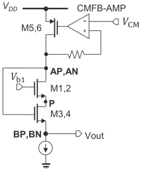
In Fig. 4, a full schematic of the proposed LNA is shown. For the amplifier stage, the driver stage is seen as a high-impedance current source because the current flow through the junction node (P) is kept constant set by the bot- tom transistors M7 and M8. The impedance of the current source is determined by the channel-length modulation ef- fect of M7 and M8. When the input signal (vIN) is single- ended (as required by ultrasound imagers) and the gate volt- age of M2 is a fixed DC bias as shown in Fig. 4, the voltage of junction node P (vP) follows the same polarity as vINbe- cause the common-mode input component appears at this node. The drain current of M2 is also generated by the swing of vP. This results in the positive output of the 1st stage (vO1P) having the same polarity as vIN and the neg- ative output having the opposite polarity. At the source- follower stage, the voltage of VO1Pand VO1N is shifted by (VTH+VOV) with M3 and M4. Here, VTHand VOVare the threshold voltage and over-drive voltage of the MOS tran- sistors, respectively. The body terminals of M3 and M4 are connected to their source terminals to avoid the body effect.
One of the important points of this structure is that it enables a high gain with a low output impedance because the maxi- mum gain is determined by the output impedance of the 1st amplifier stage, and a low output impedance is achieved in the driver stage.
The proposed stacked architecture needs to be care-
Fig. 4 Schematic of proposed LNA circuit.
fully designed in consideration of the bias point and voltage swing at each node. A simple guideline for the design is given as follows. As previously described, the polarity of the voltage swing at the drain and source is the same for M2 and M4 but opposite for M1 and M3. Therefore, the con- straint for operating the transistors in the saturation region for M1 and M3 is more stringent than that for M2 and M4.
The condition for operating in the saturation region for M1, M3, and M5 is described as (1) and (2).
VOV1+vOUT
+VOV2+vP+VOV3+vOUT+VOV4<VDD (1) vP= vIN
2 , vOUT =G
2vIN (2)
Here, VOVX(X=1∼4) is over-drive voltage of each tran- sistor as denoted in Fig. 4 and vOUT, vP, and vINare voltage swing at the output of driver, node P and input of ampli- fier stage respectively. G is the differential voltage gain of the amplifier. In (1), the voltage gain of the source follower (M3, M4) was approximately regarded as one, which is rea- sonable when the body terminal is connected to the source terminal. (1) and (2) result in the following Eq. (3).
VOV1+ G+1 2
!
vIN+VOV2+VOV3+VOV4<VDD (3) When applying VDD =1.8 V, VOVX =0.2 V, and G=
10, (3) results in vIN < 100 mV, giving upper limit of the input range. We also need to consider the voltage shift by the source follower as follows.
VO2=VO1−VTH−VOV2 (4) Due to this relation, the 1st-stage common-mode level (VO1) is determined by the output common-mode level (VO2). Also, the voltage swing at junction node P and the output node is sandwiched by VO1 and VO2, which gives Eq. (5) and hence (6) by combining with (4).
VO2+vOUT
2 +VOV2+vP<VO1−vOUT
2 −VOV3 (5) vOUT< VTH−VOV3
1+1/G ≈VTH−VOV3 (6)
The Eq. (6) means that the maximum output swing is determined by the threshold voltage of M3 and M4. Thus, to achieve the maximum swing of vOUT =0.5 V, the threshold voltage needs to be equal to or larger than 0.7 V. From these analyses, when VOVX =0.2 V and VTH =0.7 V, the appro- priate bias voltage can be decided to be about VO2=0.45 V and VO1 = 1.35 V. Here, VO1is controlled to be the same voltage as common-mode bias VCM by a common-mode- feedback amplifier (CMFB-AMP) and load PMOS transis- tors (M5, M6) as shown in Fig. 4. Once VO1is set by VCM, VO2 is also biased automatically with the relationships in accordance with Eq. (4).
Next, the effects of process, voltage and temperature variations are discussed. The proposed LNA is affected by variation of the threshold voltage of MOS transistors (due to process or temperature variations) more significantly than by variation of the over-drive voltage (VOVX), as long as the bias circuit is designed to keep the current constant against the variations. As shown in (6), the maximum output swing is determined by the threshold voltage and becomes smaller with the lower threshold voltage. Therefore, the output range and hence the input range of the proposed LNA need to be set by considering the minimum threshold voltage un- der the variations. In addition, when the power supply volt- age decreases, the input range can be reduced based on (3).
It should also be noted that the source follower serves not only as a driver but also as a level shifter. The de- lay stage includes parallel samplers which are composed of MOS switches and capacitors as shown in Fig. 5(a). A band- width of the samplers is determined by an output impedance (ROUT) of the LNA, an on-resistance of the sampling switch (RSW) and a capacitance of the sampling capacitor in each sampler. The low-level voltage (VO2) brought by the level- shift function of the source follower makes it possible to use NMOS switches instead of CMOS switches because the on-resistance of NMOS is lower when the signal stays in low level as shown in Fig. 5(b). This is additional advantage for reducing the area of the ultrasound beamformer IC since there are many sampling switches in the delay stage.
Fig. 5 Level shift function for facilitating the delay stage. (a) Load cir- cuit of LNA. (b) Bias voltage and on-resistance of NMOS sampling switch.
3. Stability Analysis
In this section, the stability of the proposed LNA is de- scribed. For differential signal component, the amplifier stage and the driver stage are isolated from each other be- cause node P serves as AC ground. Therefore, the common- mode stability is addressed here. Figure 4 can be simpli- fied as Fig. 6 for common-mode signal component. The common-mode voltage at the node AP (AN) which is output node of the amplifier stage is determined by a local feedback loop of a CMFB-AMP and M5 (M6). An important point is that the voltage variation at node AP (AN) is not fed back by M3 (M4) because the voltage at node BP (BN) which is output node of the driver stage follows to match the voltage for keeping the drain current of M4 (M3). Variation in the common-mode voltage at the input node is also absorbed by voltage change at node P. Therefore, there is no addi- tional sensitive feedback loop in this current-reuse architec- ture compared with single-stage differential common-source
Fig. 6 Simplified schematic for common mode stability analysis.
amplifiers. Therefore, design for stability can be treated in the same manner as an open-loop differential LNA.
4. Measurement Results
The proposed LNA was designed and fabricated in a 0.18- µm SOI CMOS process. Figure 7 shows a photo of the fabricated chip. The core area of a single proposed LNA including the CMFB-AMP is 70µm × 80µm. Figure 8 shows a set up for measuring the fabricated LNA. The fab- ricated chip is packaged in QFP44. The input signal is sup- plied to the LNA from arbitrary/function generator (Agi- lent: 33500B) through the on-chip TR-SW [4]. The out- put signal of the LNA is buffered by an on-chip monitor- ing buffer (MON-BUFFER) and measured by a differential probe (Agilent: 1141A) and spectrum analyzer (Keysight:
N9030B). In the following measured result, input voltage is defined as voltage at an input terminal on the evalua- tion board. The reason of using MON-BUFFER is to avoid a parasitic capacitance of evaluation board. Because the LNA is designed to drive a switched capacitor in the de- lay stage, which is usually a few pF or less, the parasitic capacitance of evaluation line is too large to evaluate a performance of the LNA without an on-chip buffer. Fig- ure 9 shows a structure of the MON-BUFFER. The MON- BUFFER is a very simple source-follower circuit composed of 5V-MOSFETs. 5V-MOSFETs are utilized to prevent a linearity of MON-BUFFER from affecting the evaluation re- sults. The equivalent input capacitance of MON-BUFFER is 1.2 pF and−3 dB cutofffrequency with 20 pF load capaci- tance is 70 MHz, which is enough bandwidth to evaluate the LNA. The gain of MON-BUFFER is−0.07 dB to−0.2 dB in 0.1 MHz–10 MHz, which affects the evaluation of the LNA performance only slightly.
The measured supply current of the LNA circuit was
Fig. 7 Die photo of proposed LNA.
Fig. 8 Measurement setup.
Fig. 9 Implemented MON-buffer for measurement.
85µA including CMFB-AMP under a supply voltage of 1.8 V. The total power consumption was 153µW, which is very suitable for ultrasound imaging systems as described in Sect. 1. Figure 10 shows the simulated and measured fre- quency response of the prototype LNA. The LNA achieved a 10-MHz cutoff at−3 dB from the peak gain of 21.9 dB in measurement results, which is well matched with simu- lation. In a real ultrasound beamformer, the signal source is the transducer element and their impedance is different from that of signal generator (50 ohm). Regarding the fre- quency characteristics, the low-frequency side is mainly af- fected by this difference of impedance. However, since the input impedance of this LNA is high, it can be adjusted to match the impedance of the transducer element by inserting a resistor between the LNA input and the ground. The sim- ulated and measured gain, 2nd and 3rd harmonic distortions versus input voltage swing are presented in Fig. 11. As men-
Fig. 10 Simulated and measured frequency response of proposed LNA.
Fig. 11 Simulated and measured performance of gain and 2nd, 3rd har- monic distortion versus input voltage swing.
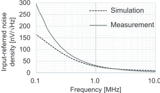
Fig. 12 Simulated and measured input-referred voltage noise density.
tioned in Sect. 2, distortion increases when the input voltage becomes close to 100 mVpp, but the 2HD increases less than the 3HD because of the differential cancellation. The 2HD was kept below−40 dBc at a 0.1-Vpp input in measurement result. A possible reason why the measured 2HD is higher than the simulation result at small input swing is mismatch in the differential architecture due to process variation. The measured input-referred noise density was 11.3 nV/√
Hz in average from 1 MHz to 10 MHz (necessary for the ultra- sound system), and the noise density of the full bandwidth is plotted in Fig. 12. The performance of the proposed LNA is compared with state-of-the-art works of bandwidth 1 MHz–
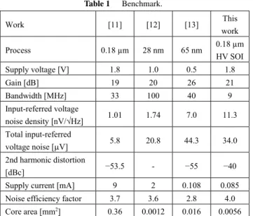
100 MHz LNA in Table 1. A noise efficiency factor (NEF) [14] is employed to compare the trade-off between power
Table 1 Benchmark.
consumption and noise performance.
NEF=Vni,rms
r 2Itot
π·UT·4kT·BW (7)
where Vni,rms is the total in-band input-referred voltage noise, Itot is the supply current,UT is the thermal voltage, k is the Boltzmann constant, T is the temperature and BW is the bandwidth of LNA, respectively. The attained power and area efficiencies are competitive or even better than prior works with much finer CMOS process.
5. Conclusion
In this paper, a low-power small-size LNA with a novel current-reuse architecture was presented for ultrasound beamformers. The proposed LNA was implemented in only 0.0056 mm2 chip area with 0.18-µm CMOS process and verified the performance of an input noise density of 11.3 nV/√
Hz, a bandwidth of 9 MHz, and a gain of 21 dB with sufficiently low supply current 85µA, which enables to increase a performance of a next-generation 3D ultrasound imaging system.
References
[1] Y. Igarashi, S. Kajiyama, Y. Katsube, T. Nishimoto, T. Naka- gawa, Y. Okuma, Y. Nakamura, T. Terada, T. Yamawaki, T. Yazaki, Y. Hayashi, K. Amino, T. Kaneko, and H. Tanaka, “Single-chip 3072-element-channel transceiver/128-subarray-channel 2-D array IC with analog RX and all-digital TX beamformer for echocardio- graphy,” IEEE J. Solid-State Circuits., vol.54, no.9, pp.2555–2567, Sept. 2019.
[2] J.-Y. Um, E.-W. Song, Y.-J. Kim, S.-E. Cho, M.-K. Chae, J. Song, B. Kim, S. Lee, J. Bang, Y. Kim, K. Cho, B. Kim, J.-Y. Sim, and H.- J. Park, “An analog-digital-hybrid single-chip RX beamformer with non-uniform sampling for 2D-CMUT ultrasound imaging to achieve wide dynamic range of delay and small chip area,” IEEE ISSCC Dig.
Tech. Papers, pp.426–427, Feb. 2014.
[3] K. Chen, H. Lee, and C.G. Sodini, “A column-row-parallel ASIC architecture for 3-D portable medical ultrasonic imaging,” IEEE J.
Solid-State Circuits, vol.51, no.3, pp.738–751, March 2016.
[4] S. Kajiyama, Y. Igarashi, T. Yazaki, Y. Katsube, T. Nishimoto, T. Nakagawa, Y. Nakamura, Y. Hayashi, and T. Yamawaki, “T/R- switch composed of 3 high-voltage MOSFETs with 12.1µW con- sumption that can perform per-channel TX to RX self-loopback AC tests for 3D ultrasound imaging with 3072-channel transceiver,”
IEEE Asian Solid-State Circuits Conference Proceedings of Techni- cal Papers, pp.305–308, Nov. 2019.
[5] J.J. Zhou and D.J. Allstot, “Monolithic transformers and their ap- plication in a differential CMOS RF low-noise amplifier,” IEEE J.
Solid-State Circuits., vol.33, no.12, pp.2020–2027, Dec. 1998.
[6] Z. Huang, C. Huang, Y. Hung, and M. Chen, “A CMOS current reused low-noise amplifier for ultra-wideband wireless receiver,”
2008 International Conference on Microwave and Millimeter Wave Technology, pp.1499–1502, Nanjing, 2008.
[7] H. Hsieh and L. Lu, “Design of ultra-low-voltage RF frontends with complementary current-reused architectures,” IEEE Trans. Microw.
Theory Techn., vol.55, no.7, pp.1445–1458, July 2007.
[8] HA.N. Karanicolas, “A 2.7-V 900-MHz CMOS LNA and mixer,”
IEEE J. Solid-State Circuits, vol.31, no.12, pp.1939–1944, Dec.
1996.
[9] B. Johnson and A. Molnar, “An orthogonal current-reuse ampli- fier for multi-channel sensing,” IEEE J. Solid-State Circuits, vol.48, no.6, pp.1487–1496, June 2013.
[10] M. Rezaei, E. Maghsoudloo, C. Bories, Y. De Koninck, and B.
Gosselin, “A low-power current-reuse analog front-end for high- density neural recording implants,” IEEE Trans. Biomed. Circuits Syst., vol.12, no.2, pp.271–280, April 2018.
[11] S. Jung, S. Hong, and O. Kwon, “Low-power low-noise amplifier using attenuation-adaptive noise control for ultrasound imaging sys- tems,” IEEE Trans. Biomed. Circuits Syst., vol.11, no.1, pp.108–
116, Feb. 2017.
[12] L. Luo, Y. Wu, J. Diao, F. Ye, and J. Ren, “Low power low noise amplifier with DC offset correction at 1 V supply voltage for ultra- sound imaging systems,” 2018 IEEE 61st MWSCAS, Windsor, ON, Canada, pp.137–140, 2018.
[13] P. Wang and T. Ytterdal, “A 54-µW inverter-based low-noise single- ended to differential VGA for second harmonic ultrasound probes in 65-nm CMOS,” IEEE Trans. Circuits Syst. II, Exp. Briefs, vol.63, no.7, pp.623–627, July 2016.
[14] M.S.J. Steyaert and W.M.C. Sansen, “A micropower low-noise monolithic instrumentation amplifier for medical purposes,” IEEE J. Solid-State Circuits, vol.22, no.6, pp.1163–1168, Dec. 1987.
Yohei Nakamura received the B.E. and M.E. degrees in electrical engineering from The University of Tokyo, Tokyo, Japan, in 2009 and 2011, respectively. In 2011, he joined the Cen- tral Research Laboratory, Hitachi, Ltd., Tokyo, where he has been engaged in analog circuit de- sign, including ADCs. Mr. Nakamura received the 2014 Young Researcher Award from the In- stitute of Electronics, Information and Commu- nication Engineers (IEICE).
Shinya Kajiyama received the B.E. de- gree from Yokohama National University, Yoko- hama, Japan, in 1995, and the M.E. degree in applied chemistry from The University of To- kyo, Tokyo, Japan, in 1997. In 1997, he joined Hitachi, Ltd., Yokohama, where he was en- gaged in the research and development of read- channel and preamplifier integrated circuits (ICs) for hard disk drives (HDDs), transceiver ICs for high-speed optical links, high-density flash memories, embedded flash memories, mi- crocontroller clocking architecture, and medical ultrasound 2-D array beamformer ICs. Mr. Kajiyama has been serving as a Technical Program Committee Member of the Custom Integrated Circuits Conference (CICC).
Yutaka Igarashi received the B.S. and M.E. degrees in electronic engineering from the Tokyo University of Science, Chiba, Japan, in 1991 and 1993, respectively. In 1993, he joined the Image and System Laboratory, Hitachi, Ltd., Yokohama, Japan, where he was dedicated to the research and development of high-frequency circuits and RFICs for digital television and cel- lular phones. Since 2013, he has been engaged in the development of ultrasound 2-D array inte- grated circuits (ICs) at the Yokohama Research Laboratory, Hitachi, Ltd.
Takashi Oshima received the B.S., M.S., and Ph.D. degrees in physics from The Univer- sity of Tokyo, Tokyo, Japan, in 1996, 1998, and 2001, respectively. He joined Central Research Laboratory, Hitachi, Ltd., Tokyo, in 2001, where he is currently a Researcher of analog and digi- tal circuits. From 2005 to 2006, he was a Visit- ing Researcher with the University of Califor- nia at Berkeley, Berkeley, CA, USA. Dr. Os- hima is a member of the Institute of Electron- ics, Information, and Communication Engineers (IEICE), the Institute of Electrical Engineers of Japan (IEEJ), IEEE and the Physical Society of Japan. He received several awards including the 2010 Best Invited Paper Award of the IEICE Electronics Society and the ISSCC2016 Outstanding Evening Session Award. He served as the Sec- retary of the IEEE Solid-State Circuits Society Japan Chapter and a Tech- nical Program Committee Member of the IEEE European Solid-State Cir- cuits Conference (ESSCIRC). He is currently a Technical Program Com- mittee Member of the IEEE International Solid-State Circuits Conference (ISSCC).
Taizo Yamawaki received the B.S. and M.S.
degrees in electronic engineering from Kyoto University, Kyoto, Japan, in 1992 and 1994, respectively. After graduating, he joined the Central Research Laboratory, Hitachi, Ltd., To- kyo, where he developed a series of commercial cellular-phone RFICs for several standards, in- cluding GSM, EDGE, WCDMA, and LTE us- ing BiCMOS and CMOS technologies. Since 2013, he has been participating as a Manager in research projects about analog front-end circuits for ultrasound probes, a variety of sensors, and dc–dc converters for auto- motive applications.
![Fig. 3 Architecture of conventional [5] and proposed current-reuse LNA.](https://thumb-ap.123doks.com/thumbv2/123deta/5632917.1501341/2.892.529.756.114.563/fig-architecture-conventional-proposed-current-reuse-lna.webp)