andYasuhiko ARAKAWA†,†††††,Fellow
SUMMARY One of the most serious challenges facing the exponential performance growth in the information industry is a bandwidth bottleneck in inter-chip interconnects. We therefore propose a photonics-electronics convergence system with a silicon optical interposer. We examined inte- gration between photonics and electronics and integration between light sources and silicon substrates, and we fabricated a conceptual model of the proposed system based on the results of those examinations. We also inves- tigated the configurations and characteristics of optical components for the silicon optical interposer: silicon optical waveguides, silicon optical split- ters, silicon optical modulators, germanium photodetectors, arrayed laser diodes, and spot-size converters. We then demonstrated the feasibility of the system by fabricating a high-density optical interposer by using silicon photonics integrated with these optical components on a single silicon sub- strate. As a result, we achieved error-free data transmission at 12.5 Gbps and a high bandwidth density of 6.6 Tbps/cm2with the optical interposer.
We think that this technology will solve the bandwidth bottleneck problem.
key words: integrated optics, integrated optoelectronics, optical devices, optical interconnections
1. Introduction
The inter-chip bandwidths in personal computers and servers have been doubling every two years [1]. For ex- ample, since a CPU for high-end servers has an overall inter-chip bandwidth of about 1.5 Tbps, which consists of 0.5 Tbps for CPU-CPU interconnects (QPI), 0.4 Tbps for CPU-memory (DDR3), and 0.6 Tbps for CPU-peripherals (PCIe 3) at this moment, the overall inter-chip bandwidth is expected to reach a 10-Tbps level by the late 2010 s. Al- though the wiring pitches in logic circuits are expected to shrink exponentially on the basis of Moore’s law, LSI I/O pad pitches, such as flip-chip pad pitches, are expected to remain large [2]. Consequently, the scaling gap between intra-chip and inter-chip is going to widen annually. This is why the line speed for inter-chip interconnects in the future will need to be much higher than that for intra-chip ones.
The required line speed is expected to exceed 40 Gbps by Manuscript received October 31, 2012.
†The authors are with Institute for Photonics-Electronics Con- vergence System Technology (PECST), Japan.
††The authors are with Photonics Electronics Technology Re- search Association (PETRA), Tsukuba-shi, 305-8569 Japan.
†††The authors are with National Institute of Advanced Industrial Science and Technology (AIST), Tsukuba-shi, 305-8569 Japan.
††††The author is with PETRA, Atsugi-shi, 243-0198 Japan.
†††††The author is with The University of Tokyo, Tokyo, 153-8505 Japan.
a) E-mail: [email protected] DOI: 10.1587/transele.E96.C.958
the late 2010 s, and nobody knows how this speed will be possible with electrical interconnects [2].
Optical interconnects with silicon photonics have been expected to solve the bandwidth bottleneck problem with LSI chips and have been investigated by many organizations [1], [3]–[7] because of the intrinsic properties of optical sig- nals, such as wide bandwidth, low latency, low power con- sumption, and low mutual interference, and because of the industrial advantages of silicon for use in the electronics in- dustry. There have been few reports, however, on inter-chip interconnects that have been made using silicon photonics and that have been fully integrated with light sources, opti- cal modulators, and photodetectors (PDs) on a single silicon substrate.
In this paper, we examine photonics-electronics inte- gration, propose a photonics-electronics convergence sys- tem with a silicon optical interposer to solve the bandwidth bottleneck problem in inter-chip interconnects, investigate optical components for the optical interposers, and demon- strate the feasibility of the system by presenting the results of data transmission experiments with the silicon optical in- terposers.
2. Photonics-Electronics Convergence System for Inter- Chip Interconnects
2.1 Integration between Photonics and Electronics Because the performance of electrical interconnects gen- erally declines with their distance more rapidly than does that of optical interconnects, it is important to place opti- cal transceivers (E/O and O/E signal converters) as close to LSIs as possible for wide-bandwidth inter-chip intercon- nects with photonic wiring. Silicon photonics is the most suitable technology for these applications because of its compactness and compatibility with LSIs.
Generally, there are three types of integration be- tween photonic and electronic circuits with silicon photon- ics: front-end integration, back-end integration, and flip- chip bonding (see cross sections in Fig. 1). The first two are monolithic integrations and the last is a hybrid integra- tion. Monolithic integration, especially front-end integra- tion, is expected to provide higher speed and lower assem- bling cost than hybrid integration, but it requires very strict CMOS compatibilities in terms of design, fabrication, and Copyright c2013 The Institute of Electronics, Information and Communication Engineers
Fig. 1 Schematic cross sections of integrations between photonic and electronic circuits.
testing. We think that it will be a long time before the tech- nology is mature enough. On the other hand, the hybrid integration allows us to choose the most suitable technology nodes separately for photonics and electronics circuits, to design, fabricate and test them separately, and then combine their good dies. This scheme can improve product yields and stimulate horizontal specialization between electronics and photonics, or between LSI chips and their inter-chip in- terconnects. Therefore, since we think that the hybrid inte- gration is the most practical choice now and in the near fu- ture, we have taken the hybrid-integration route to photonic- electronic integration for inter-chip interconnects.
2.2 Light Source Integration
Considering light source arrangement in optical inter-chip interconnects, we had first to choose off-chip sources or on- chip sources. Although the off-chip light sources are more flexible than the on-chip ones, they require highly precise optical connectors to get optical power from the off-chip light sources into the substrate. Because we think that these optical connectors are not practical for large scale intercon- nects, we have chosen on-chip light sources. There are two types of integrations for on-chip light sources: monolithic integration with silicon or germanium lasers, and hybrid integration with compound semiconductor lasers. Mono- lithically integrated Ge-on-Si lasers were recently reported [8], but their efficiency and output optical power are low for inter-chip interconnects applications. We have therefore chosen hybridly integrated lasers. There are two types of compound semiconductor lasers for optical interconnects:
edge emitting lasers and vertical cavity surface emitting lasers (VCSELs). Because VCSELs can’t keep their sin- gle mode operation when the optical output is high, we have chosen edge emitting lasers. There are also two types of hy- brid lasers in terms of optical coupling structures between the active waveguide and the silicon waveguide: evanescent- coupled lasers [9], and butt-coupled lasers [10]. Although the evanescent-coupled lasers have higher tolerance against alignment error when the compound semiconductor chips are mounted on the silicon substrate than the butt-coupled ones, we think their efficiency and output optical power are not high enough for inter-chip interconnects with optical splitters. We have therefore chosen to use butt-coupled hy-
Fig. 2 Conceptual model of photonics-electronics convergence system for inter-chip interconnects.
brid lasers for inter-chip interconnect applications.
2.3 Conceptual Model
The conceptual model of the photonics-electronics con- vergence system for inter-chip interconnects is outlined in Fig. 2. The upper-left LSI chip on the silicon optical inter- poser has been removed to enable the substrate surface area that it covered to be seen. Optical splitters, optical modula- tors, and PDs are monolithically integrated on a silicon sub- strate, arrayed LDs are hybridly integrated on the substrate, and these optical components are optically linked to each other via silicon optical waveguides. Together they form a silicon optical interposer. Bare LSI chips are mounted on the interposer and are electrically connected to the optical modulators and PDs by flip-chip bonding. That is, electric circuits (the bare LSI chips) and photonic circuits (the opti- cal interposer) are integrated hybridly.
The inter-chip interconnects with the silicon optical in- terposers operate as follows. Arrayed LDs are driven simul- taneously by DC current. The CW light from each LD is divided by an optical splitter and launched into an optical modulator. The optical modulators are directly driven by transmitter circuits in one LSI. The modulated optical sig- nals propagate along inter-chip optical waveguides and are the input for PDs under another LSI. The electrical signals from those PDs are the input for receiver circuits in the LSI that the PDs are under.
This system enables us to replace the conventional electronic wires on a printed circuit board (PCB) with the optical interconnects on a silicon substrate, which is one hundredth the size of a PCB. This silicon optical interposer has wide bandwidth capabilities due to the properties of its optical signals. Since the silicon substrates can be fabri- cated using a CMOS-compatible process, they have quite high density and are low in cost. Furthermore, because this system is optically complete and closed without any optical inputs or outputs, users do not have to worry about any op-
optical interposer that mainly consisted of silicon optical waveguides, silicon optical modulators, germanium PDs, LDs, and spot-size converters (SSCs) between the LDs and the silicon optical waveguides. Configurations and charac- teristics of these optical components were investigated as follows.
3.1 Silicon Optical Waveguides
Generally, there are two types of silicon optical waveguides in terms of their core cross section shapes: rib-shaped and rectangular. The propagation loss of the rib-shaped waveg- uides is lower than that of the rectangular ones, but the rib- shaped waveguides pose difficulties in the fabrication pro- cess in that we have to stop etching the silicon layer to leave a precisely thin silicon slab. We think this issue is critical in terms of yields in mass production, especially, as will be ex- plained later, for the yields of optical modulators. We have therefore chosen rectangular core waveguides for our silicon optical interposers, and we have developed fine lithography and etching processes in our clean room for rectangular core waveguides. As a result, with a rectangular core that was 480-nm wide and 220-nm thick we have obtained propaga- tion losses as low as 4 dB/cm at a 1530-nm wavelength.
3.2 Silicon Optical Modulators
There were a lot of research activities regarding silicon op- tical modulators using the carrier plasma effect in PIN or PN diode [11]–[13], and most of them used a doped sili- con slab in the rib-shaped waveguides to make electric con- tact between their waveguide core and metal electrodes. In these cases, the gap between P- and N-doping areas should be wider than the width of the optical mode profile to pre- vent optical absorption loss due to the highly doped carriers.
The optical mode profile in these rib-shaped waveguides ex- tended to the slab area, and a thicker slab caused a wider mode profile and P-N gap. The wider P-N gap made the resistivity higher and made the modulation efficiency and modulation speed lower. Because optical modulator char- acteristics such as optical loss, modulation efficiency, and speed were sensitive to the slab thickness in this way, we had to stop etching the silicon layer to leave a precisely thin silicon slab.
To overcome these design and fabrication difficulties, we have proposed a novel structure for the electric contact between the waveguide core and electrodes instead of the silicon slab. Figure 3(a) is a schematic of the structure of
Fig. 3 Proposed optical modulator.
our proposed optical modulators [14]. The optical mod- ulator is a Mach-Zehnder (MZ) interferometer composed of phase shifters and multimode interference (MMI) cou- plers. The phase shifters, which have side-wall gratings on both sides of the waveguide core in order to enable electric contact between the core and metal electrodes, can change their refractive indices by the carrier plasma effect in lat- eral PIN diode structures. Figure 3(b) shows microscope and SEM images of the fabricated modulator. Because the waveguides had a uniform thickness of silicon over the en- tire modulator, the etching process was much easier than that with rib-shaped waveguides. Moreover, this structure enabled stronger lateral optical mode confinement, a nar- rower optical mode profile, a narrower P-N gap, lower resis- tivity, higher efficiency, and higher speed than the modula- tors with rib-shaped waveguides. The pitch of the side-wall grating was designed so that the stop-band wavelength was much shorter than the operation wavelength. The interaction length of the phase shifter was 250μm.
The measured DC response of the optical modula- tor is plotted in Fig. 4. The π-phase shift voltage (Vπ) was 0.13 V and the modulation efficiency (Vπ*L) was 0.003 Vcm, which is four times as high as the efficiency of our previous modulator with rib-shaped waveguides [7].
The extinction ratio (ER) was 14.3 dB.
3.3 Germanium Photodetectorsa
There are generally two types of germanium PDs that we can monolithically integrate on a silicon substrate: PIN- PDs and metal-semiconductor-metal (MSM) PDs. MSM- PDs require fewer fabrication steps but finer patterning and alignment than PIN-PDs. In this work we fabricated MSM- PDs for the silicon optical interposers. Figure 5(a) is a
Fig. 4 DC response of optical modulator.
Fig. 5 Structure and images of MSM-PD.
schematic of the structure of our germanium MSM-PD [15], and Fig. 5(b) also shows microscope and SEM images of it.
The measured frequency responses of PDs with 4- to 10-V biases are plotted in Fig. 6. The 3-dB cutofffrequen- cies were 6 GHz with a 4-V bias voltage and 9 GHz with a 10-V bias voltage. The dark current of the PDs was about 1μA. The photo to dark current ratio was higher than 30 dB.
The responsivity was 1 A/W.
3.4 Arrayed Laser Diodes
The LD chip was a 13-channel InGaAsP LD array with a 30-μm channel pitch. Each channel was a Fabry-Perot type LD with a spot-size converter. The chip had a single pair of electrodes for all 13 channels, which simultaneously emit- ted 1530-nm light. The near field pattern and output inten- sity of the 13-channel LD array are shown in Fig. 7. The
Fig. 6 Frequency responses of PDs.
Fig. 7 Near field pattern and output intensity of LD array.
Fig. 8 Schematic structure and SEM images of a trident SSC.
output power uniformity across all the channels was better than 0.7 dB.
3.5 Spot-Size Converters
Spot-size converters between the LDs and silicon optical waveguides are key components for the silicon optical inter- posers in terms of their optical power budget and fabrication process simplicity. We previously had two types of SSC:
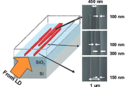
tapered silicon waveguides and SiON waveguides. The for- mer did not need additional processes but had large coupling loss [7], and the latter had low coupling loss but needed ad- ditional processes [10]. We later introduced a novel SSC called a trident [16]. The schematic structure and SEM im- ages of the trident SSC are shown in Fig. 8. It consists of only three narrow silicon waveguides fabricated without ad- ditional process. Measured coupling losses between the LD and the trident SSC with various alignment deviations in the
Fig. 9 Measured coupling loss between an LD and trident SSC.
horizontal and vertical directions are plotted in Fig. 9. We obtained coupling losses as low as 2.3 dB, and the alignment error tolerance up to 1-dB loss increase was about±0.9μm in both directions, which was large enough for our align- ment precision (±0.5μm) with a passive alignment tech- nique [17].
4. Fabrication of Silicon Optical Interposers
The silicon optical interposers were fabricated from 4-inch silicon-on-insulator (SOI) wafers in the Super Clean Room at AIST Tsukuba West by using CMOS process technology.
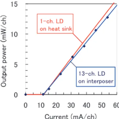
The silicon optical waveguides were formed by electron- beam lithography and dry etching. The epitaxial germa- nium mesas for the PDs were selectively grown on the sil- icon waveguide by chemical vapor deposition. The waveg- uides, modulators, and PDs were covered with the SiO2up- per cladding layer by chemical vapor deposition. The wave- guide endfaces and the pedestals for the LD mount were formed by dry etching. An arrayed LD chip was hybridly integrated on the substrate with a passive alignment tech- nique [17]. As a result, the LD array was butt-coupled to the silicon waveguide array via the trident SSC array. The I-L characteristics of the LDs measured without tempera- ture control are plotted in Fig. 10, where the blue line shows the I-L characteristics of the 13-ch. arrayed LD hybridly in- tegrated on the interposer and the red line shows that of a 1-ch. LD on a heat sink. Since all 13 channels were driven simultaneously, the actual current injected into the arrayed LD chip was 13 times of the value in the horizontal axis.
Although the heat generation in the 13-ch. LD was 13 times as high as that in the 1-ch. LD, both I-L characteristics had about the same threshold currents and slope efficiencies, and no output power saturations up to 10 mW or more per chan- nel. That suggests this hybridly integrated arrayed LD had a quite high heat dissipation capability. We think that the high output power and high heat dissipation capabilities are ad- vantages of our butt-coupled hybrid lasers over evanescent- coupled ones.
Figure 11 shows a photograph of a silicon optical inter- poser fabricated on a 5 mm×5 mm substrate. A trident SSC array, a 1×4 optical splitter, an optical modulator array, and a PD array were monolithically integrated on a single silicon
Fig. 10 I-L characteristics measured without temperature control.
Fig. 11 Photograph of a silicon optical interposer.
substrate, and a 13-channel arrayed LD chip was hybridly integrated on the substrate. These optical components were optically linked to each other via a silicon optical waveguide array.
5. Data Transmission Experiments
Data transmission experiments with the silicon optical inter- posers were carried out as follows. All 13 channels of the arrayed LD were simultaneously driven by a single DC cur- rent. The CW light from the LD was divided into four by the 1×4 optical splitter and each of them launched into the op- tical modulator. RF input signals were pre-emphasized by a differentiator consisting of passive RC circuits and were modulator input. The voltage amplitude after pre-emphasis was 3.4 V peak to peak. The modulated optical signals prop- agated along the optical waveguides and were led to the PD array, which converted them into electrical signals.
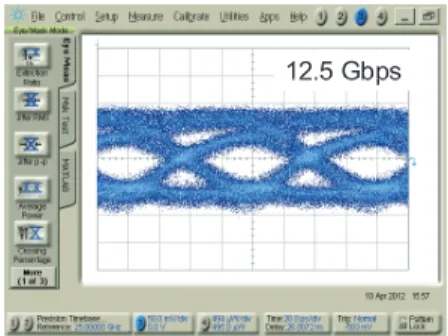
The measured eye diagram of PD output at 12.5-Gbps NRZ with a 27-1 pseudo-random binary sequence (PRBS) via 1 ×4 optical splitter is shown in Fig. 12. The clear eye opening suggests that the optical links were capable of data transmission at 12.5 Gbps. The measured bit error rates (BER) for the 12.5-Gbps PRBS are plotted in Fig. 13. We confirmed that BER was less than 10−12when the PD input power was more than−5 dBm. Error-free data transmission
Fig. 12 Eye diagram of PD output for 12.5-Gbps NRZ PRBS.
Fig. 13 Bit error rates for 12.5-Gbps NRZ PRBS.
at 12.5 Gbps via the 1×4 optical splitter was achieved. Be- cause this system was optically complete and closed, we did not need to align fibers, control polarization, or control tem- perature throughout the experiments.
The optical power budget per channel is summarized in Table 1. The optical waveguide length was about 5.3 mm.
The overall optical loss was 18 dB, including inherent 6-dB branching loss and 3-dB modulation loss. Because of the novel trident SSC with a quite low coupling loss, we ob- tained an optical power margin that enabled us to introduce the 1×4 optical splitter. These results suggest that integrat- ing a 13-channel arrayed LD, 13 1×4 optical splitters, and 52 modulators and PDs enables the optical interposer on a single silicon substrate to achieve a bandwidth of 650 Gbps.
Furthermore, we can increase the optical waveguide length to 20 mm by removing the 1×4 optical splitters.
The per-channel footprints of the optical components are listed in Table 2. The per-channel footprint of laser diode was also split into four due to the 1×4 optical splitter. The total footprint was 0.19 mm2per channel, meaning we could achieve a bandwidth density of 6.6 Tbps/cm2with a channel line rate of 12.5 Gbps. We would like to emphasize that we achieved this high bandwidth density with MZ modulators, which are generally larger but more practical than ring mod- ulators.
Since the typical CPU die is about 2 cm2 in area, we can obtain an overall inter-chip bandwidth of 10-Tbps level, which will satisfy the required bandwidth in the late 2010 s as mentioned previously, by using the silicon optical inter- posers. About two-thirds of the total footprint was occu-
Table 1 Optical power budget.
Table 2 Per-channel footprints of optical components.
pied by electrode pads in these experiments. And we have already reported individual optical modulators and PDs, which operate faster than 40 Gbps and can be integrated on the silicon optical interposer [18], [19]. Therefore we ex- pect to improve the bandwidth density further with the faster components and smaller pads in the near future.
6. Conclusion
We proposed a photonics-electronics convergence system with a silicon optical interposer in order to solve the band- width bottleneck problem that inter-chip interconnects have.
We examined integration between photonics and electronics and integration between light sources and silicon substrates, and we fabricated a conceptual model of the proposed sys- tem based on the results of those examinations. We also investigated the configurations and characteristics of opti- cal components for the silicon optical interposer: silicon optical waveguides, silicon optical modulators, germanium photodetectors, arrayed laser diodes, and spot-size convert- ers. We then demonstrated the feasibility of the system by fabricating a high density optical interposer by using sili- con photonics integrated with these optical components on a single silicon substrate. As a result, we achieved error-free data transmission at 12.5 Gbps and high bandwidth density of 6.6 Tbps/cm2 with the optical interposer. We think that this technology will solve the bandwidth bottleneck prob- lem.
Acknowledgments
This research is supported by the Japan Society for the Pro-
Block, M.R. Reshotko, and P.L.D. Chang, “Optical technology for energy efficient I/O in high performance computing,” IEEE Com- mun. Mag., vol.48, no.10, pp.184–191, Oct. 2010.
[2] International Technology Roadmap for Semiconductors 2009 Edi- tion, Assembly and Packaging, Table AP2 and AP3.
[3] L. Chen, K. Preston, S. Manipatruni, and M. Lipson, “Integrated GHz silicon photonic interconnect with micrometer-scale modula- tors and detectors,” Opt. Express, vol.17, no.17, pp.15248–15256, Aug. 2009.
[4] K. Raj, J.E. Cunningham, R. Ho, X. Zheng, H. Schwetman, P. Koka, M. McCracken, J. Lexau, G. Li, H. Thacker, I. Shubin, Y. Luo, J.
Yao, M. Asghari, T. Pinguet, J. Mitchell, and A.V. Krishnamoorthy,
“ ‘Macrochip’ computer systems enabled by silicon photonic inter- connects,” Proc. SPIE, vol.7607, pp.1–16, 2010.
[5] G. Kim, J.W. Park, I.G. Kim, S. Kim, S. Kim, J.M. Lee, G.S.
Park, J. Joo, K.S. Jang, J.H. Oh, S.A. Kim, J.H. Kim, J.Y. Lee, J.M. Park, D.W. Kim, D.K. Jeong, M.S. Hwang, J.K. Kim, K.S.
Park, H.K. Chi, H.C. Kim, D.W. Kim, and M.H. Cho, “Low- voltage high-performance silicon photonic devices and photonic in- tegrated circuits operating up to 30 Gb/s,” Opt. Express, vol.19, no.27, pp.26936–26947, Dec. 2011.
[6] X. Zheng, Y. Luo, J. Lexau, F. Liu, G. Li, H. Thacker, I. Shubin, J.
Yao, R. Ho, J.E. Cunningham, and A.V. Krishnamoorthy, “2-pJ/bit (On-Chip) 10-Gb/s digital CMOS silicon photonic link,” IEEE Pho- tonics Technol. Lett., vol.24, no.14, pp.1260–1262, July 2012.
[7] Y. Urino, T. Shimizu, M. Okano, N. Hatori, M. Ishizaka, T.
Yamamoto, T. Baba, T. Akagawa, S. Akiyama, T. Usuki, D.
Okamoto, M. Miura, M. Noguchi, J. Fujikata, D. Shimura, H.
Okayama, T. Tsuchizawa, T. Watanabe, K. Yamada, S. Itabashi, E.
Saito, T. Nakamura, and Y. Arakawa, “First demonstration of high density optical interconnects integrated with lasers, optical modula- tors and photodetectors on single silicon substrate,” Opt. Express, vol.19, no.26, pp.B159–B165, Dec. 2011.
[8] R.E. Camacho-Aguilera, Y. Cai1, N. Patel, J.T. Bessette, M.
Romagnoli, L.C. Kimerling, and J. Michel, “Germanium Laser: A CMOS compatible light emitter,” Proc. 9th Internat. Conf. on Group IV Photonics, FB1, Aug. 2012.
[9] A.W. Fang, H. Park, O. Cohen, R. Jones, M.J. Paniccia, and J.E.
Bowers, “Electrically pumped hybrid AlGaInAs-silicon evanescent laser,” Opt. Express, vol.14, no.20, pp.9203–9210, Oct. 2006.
[10] T. Shimizu, N. Hatori, M. Okano, M. Ishizaka, Y. Urino, T.
Yamamoto, M. Mori, T. Nakamura, and Y. Arakawa, “High density hybrid integrated light source with a laser diode array on a silicon optical waveguide platform for inter-chip optical interconnection,”
Proc. 8th Internat. Conf. on Group IV Photonics, ThB5, Sept. 2011.
[11] L. Liao, A. Liu, D. Rubin, J. Basak, Y. Chetrit, H. Nguyen, R.
Cohen, N. Izhaky, and M. Paniccia, “40 Gbit/s silicon optical mod- ulator for high speed applications,” Electron. Lett., vol.43, no.22, pp.1196–1197, Oct. 2007.
[12] D.J. Thomson, F.Y. Gardes, Y. Hu, G. Mashanovich, M. Fournier, P. Grosse, J.-M. Fedeli, and G.T. Reed, “High contrast 40 Gb/s op- tical modulation in silicon,” Opt. Express, vol.19, no.12, pp.11507–
11516, June 2011.
[13] P. Dong, L. Chen, and Y.-k. Chen, “High-speed low-voltage single- drive push-pull silicon Mach-Zehnder modulators,” Opt. Express, vol.20, no.6, pp.6163–6169, March 2012.
[14] S. Akiyama, T. Baba, M. Imai, T. Akagawa, M. Takahashi, N.
size convertor for hybrid integrated light sources on photonics- electronics convergence system,” Proc. 9th Internat. Conf. on Group IV Photonics, ThB2, Aug. 2012.
[17] N. Fujioka, T. Chu, and M. Ishizaka, “Compact and low power con- sumption hybrid integrated wavelength tunable laser module using silicon waveguide resonators,” J. Lightwave Technol., vol.28, no.21, pp.3115–3120, Nov. 2010.
[18] S. Akiyama, T. Baba, M. Imai, T. Akagawa, M. Noguchi, E. Saito, Y. Noguchi, N. Hirayama, T. Horikawa, and T. Usuki, “50-Gb/s sil- icon modulator using 250-μm-long phase shifter based-on forward- biased pin diodes,” Proc. 9th Internat. Conf. on Group IV Photonics, ThC2, Aug. 2012.
[19] J. Fujikata, M. Noguchi, M. Miura, D. Okamoto, T. Horikawa, and Y. Arakawa, “45 GHz bandwidth of Si waveguide-integrated PIN Ge photodiode, and its zero-bias voltage operation,” Exten. Abst. of Internat. Conf. on Solid State Devices and Materials, pp.578–579, Sept. 2012.
Yutaka Urino received the B.E. degree in communication engineering and M.E. degree in electronic engineering from Tohoku University, Japan in 1985 and 1987, respectively. He joined NEC Corporation in 1987, where he has been engaged in the research and development of op- tical waveguide devices and subsystems. He is currently a chief researcher in PETRA tem- porarily.
Yoshiji Noguchi received the B.S. degrees in Chemical Engineering from Muroran Insti- tute of Technology, Muroran, Japan in 1985. He joined Texas Instruments Japan Limited in 1985, where he was engaged in the process integra- tion technology for VLSIs. In 2010, he moved to the Innovation Center for Advanced Nanode- vices (ICAN), AIST. He is now engaged in the development of dry etching technology and pro- cess integration for PECST Project and Quan- tum Information Processing Project.
Nobuaki Hatori received the B.Ed. degree from Tokyo Gagugei University in 1993, and M.E. degrees and Ph.D. in Engineering from To- kyo Institute of Technology, Japan in 1995 and 1998, respectively. He joined Fujitsu Labora- tories Ltd. in 1999, where he has been engaged in the research and development of semiconduc- tor laser and semiconductor optical amplifier de- vices. He is currently a chief researcher in PE- TRA temporarily. He is a member of the IEEE.
Masashige Ishizaka received the M.S. de- gree in 1988 from the Interdisciplinary Grad- uate School of Engineering Sciences, Kyushu University, Japan. In 1988, he joined NEC, and engaged in R&D mainly on optical com- munication devices. He is currently a princi- pal researcher in PETRA temporarily. His cur- rent research interests include the integration of light sources and silicon photonic circuits for photonics-electronics convergence system.
Tatsuya Usuki received the B.S., M.S., and Ph.D. degrees in Department of Applied Physics from Osaka University, Japan in 1986, 1988, and 1991, respectively. He joined Fujitsu Lab- oratories Ltd. in 1991, where he has been en- gaged in research of semiconductor physics and development of novel electron devices. From July 2005 to March 2009, he was a specially ap- pointed professor with the Institute of Industrial Science, the University of Tokyo. From May 2010, he is currently a chief researcher with PE- TRA. He is a member of the Japan Society of Applied Physics, IEEE Elec- tron Device Society, and American Physical Society.
Junichi Fujikata received his B.E. and M.E.
degrees in material engineering from the Uni- versity of Tokyo, Japan in 1991 and 1993, re- spectively. He joined NEC laboratories in 1993 and has engaged in studies on magnetic materi- als and devices, and recently engages in studies on silicon photonics. From 2010, he joined PE- TRA as a leader of Ge photodetector research team. He is a member of the Japan Society of Applied Physics, and IEEE Photonics Confer- ence Committee.
Koji Yamada received his B.E., M.E. and Ph.D. degrees in nuclear engineering from Kyu- shu University, Japan in 1986, 1988 and 2003, respectively. He joined NTT laboratories in 1988 and has engaged in studies on synchrotron light sources, and recently engages in studies on silicon photonics. He is now a senior research engineer, distinguished technical member and group leader of silicon nanotechnology research group in Microsystem Integration Laboratories, NTT. From 2010, he also joined PETRA as a leader of photonic wiring and waveguide research team. He is a member of the Japan Society of Applied Physics, the Atomic Energy Society of Japan, the Particle Accelerator Society of Japan, and IEEE.
Tsuyoshi Horikawa is the deputy di- rector of the Innovation Center for Advanced Nanodevices (ICAN), AIST. He received the B.S. degree and the M.S. degree in chemistry from Shizuoka University, Japan (1983) and from Kyoto University, Japan (1985), respec- tively. He joined the Materials and Electronic Devices Laboratory, Mitsubishi Electric Corp, and then moved to AIST. His research interests include materials science and process technol- ogy in electronics and silicon photonics. He has been with PECST project since 2010. He is a member of the IEEE Photon- ics Society and the Japan Society of Applied Physics.
Takahiro Nakamura received the B.E., M.E., and D.E. degrees in Electrical Engineer- ing from Osaka University, Japan in 1986, 1988, and 2005, respectively. He joined NEC Corpo- ration in 1988, where he has been engaged in the research and development of laser diodes. He is currently a chief manager in PETRA temporar- ily.
Yasuhiko Arakawa received his B.E., M.E., and Ph.D. degree in Electronics and Electrical Engineering from the University of Tokyo in 1975, 1977 and 1980, respectively. In 1980, he joined the University of Tokyo as an assistant professor and became a full professor in 1993.
He is currently the director of Research Center for Photonics Electronics Convergence, Institute of Industrial Science and the director of Institute for Nano Quantum Information Electronics, the University of Tokyo. He is a member of Science Council of Japan, a Vice President of ICO, the Asian Regional Editor in Chief of NJP, and a member of the Joint APL-JAP Editorial Board. He has been awarded Fellows of IEEE, OSA, and JSAP. His major research fields include physics, growth, and photonics applications of the quantum dot. He is leading a national project named Photonics and Electronics Convergence System Technology (PECST) of the FIRST program. Prof.
Arakawa received several major awards including Leo Esaki Award (2004), IEEE/LEOS William Streifer Award (2004), Fujiwara Award (2007), Prime Minister Award (2007), Medal with Purple Ribbon (2009), IEEE David SarnoffAward (2009), C&C Award (2010), Welker Award (2011), and OSA Nick Holonyak Jr. Award (2011).