STUDY OF WAVEGUIDE OPTICAL ISOLATOR
EMPLOYING NONRECIPROCAL RADIATION MODE
CONVERSION FOR Si PHOTONICS
SALINEE CHOOWITSAKUNLERT
Student ID: nb16503
Major: Functional Control Systems
Supervisor
Prof. Hideki Yokoi
A thesis submitted in fulfilment of the
requirements for the award of the degree of
Doctor of Engineering
CANDIDATE’S DECLARATION
It is hereby declared that this thesis or any part of it has not been submitted elsewhere
for the award of any degree or diploma.
Signed:
(Salinee Choowitsakunlert)
Student No.: NB 16503
Certified by:
Dedicated
To
Acknowledgements
Beyond anything, I would like to express my deepest gratitude and sincere appreciation to my parent, for their encouragement, support and love throughout my life, for which my mere expression of thanks likewise does not suffice.
I would like to express my appreciation and gratitude to many individuals for their assistance and contributions towards the success of this research study. Especially I am extremely delighted to express my indebtedness and deepest sense of gratitude to my supervisor Prof. Hideki Yokoi, Department of Electronic Engineering, Shibaura Institute of Technology (SIT), Japan, for his valuable and constructive suggestions during the planning and development of this research work. His willingness to give his time so generously has been very much appreciated. I am grateful to Prof. Dr. Kazuyoshi Ueno (SIT), Prof. Dr. Hiroyasu Ishikawa (SIT), Prof. Dr. Yoshikazu Koike (SIT) and, Prof. Katsumi Nakatsuhara (Kanagawa Institute of Technology), for their kind agreement in reviewing my dissertation.
I express my gratitude to Prof. Dr. Tetsuya Mizumoto (Tokyo Institute of Technology), Assoc. Prof. Dr.
Nobuhiko Nishiyama (Tokyo Institute of Technology) and, Assoc. Prof. Dr. Yuya Shoji (Tokyo Institute of
Technology), for fruitful discussions and support my research for fabricating the waveguide structure.
I express my gratitude to Prof. Dr. Tadatomo Suga (The University of Tokyo), for fruitful discussions and support my research for fabricating the magneto-optic waveguide on the silicon-on-insulator substrate by surface activated bonding.
I would like to offer a very special thanks to Assoc. Prof. Dr. Rardchawadee Silapunt (King Mongkut’s University of Technology), for her valuable time, advices and encouragement.
Abstract
An optical isolator is an indispensable device in optical communication systems since it can protect active photonic devices from unwanted reflected light. Magnetic garnet crystals are necessary to construct the optical isolator owing to their large magneto-optic coefficient and low absorption loss in the near infrared region. In decade ago, optical isolators with a Si guiding layer have been researched widely. The author has investigated two types of the optical isolator with the Si guiding layer, employing a nonreciprocal guided-radiation mode conversion. First, the optical isolator utilizes a magneto-optic waveguide with a crystalline Si guiding layer. The magneto-optic waveguide is fabricated by bonding technique between a magnetic garnet and silicon-on-insulator (SOI) structure. Last, the optical isolator consists of an amorphous Si guiding layer deposited on a magnetic garnet cladding layer. Therefore, in both cases, the optical isolator is composed of a magneto-optic waveguide with the Si guiding layer and the magnetic garnet cladding layer.
In order to realize the magneto-optic waveguide with a crystalline Si guiding layer, surface activated bonding and adhesive bonding were considered. By using these techniques, Si and a magnetic garnet can be connected with each other at low temperature. The optical isolator employing the nonreciprocal guided-radiation mode conversion was designed at a wavelength of 1.55 µm. The nonreciprocal phase shift was calculated in the magneto-optic waveguide with a magnetic garnet / Si / SiO2 structure. It was
confirmed that the largest nonreciprocal phase shift was obtained when the thickness of the Si guiding layer is 200 nm. The relationship of waveguide parameters for isolator operation was investigated. By using bonding technique, there is concern over a gap generated between the Si guiding layer and the magnetic garnet cladding layer. The nonreciprocal phase shift was calculated when the gap existed in the magneto-optic waveguide and the relationship of waveguide parameters were clarified for various gaps. The magneto-optic waveguides were fabricated by surface activated bonding and adhesive bonding.
simulating the electric field of TM guided mode and that of TE radiation mode. The magneto-optic waveguide with a-Si:H guiding layer was fabricated and evaluated.
The temperature dependence of the optical isolator employing a nonreciprocal guided-radiation mode conversion was investigated. The optical isolator consists of a rib-type magneto-optic waveguide with a-Si:H guiding layer. The relationship of rib height and rib width for the isolator operation was clarified for various operating temperatures. Refractive indices of layers in the magneto-optic waveguide were considered since proper refractive indices can circumvent deviation of the waveguide parameters due to the temperature shift. The results show that athermal operation can be achieved by the negative temperature dependence of the refractive index of the upper cladding layer, and the relationship of waveguide parameters varies only slightly with the selected upper cladding layer. As for the candidate of the upper cladding layer of the magneto-optic waveguide, TiO2 and C6H11CH3 compound were
Contents
Pages
Acknowledgements
I
Abstract
II
Contents
IV
List of Figures
IX
List of Tables
XIII
List of Publications
XIV
Ch1: Background
1
1.1 Introduction
1
1.2 Optical nonreciprocal devices
3
1.2.1 Bulk optical isolator
3
1.2.1.1 Polarization-dependent type
3
1.2.1.2 Polarization-independent type
4
1.2.2 Waveguide optical isolator
5
1.3 Si photonics
10
1.4 Waveguide optical isolator for Si photonics
12
1.5 Organization of the dissertation
15
Ch2: Theories
22
2.1 Propagation of light wave
22
2.2 Garnet crystal
24
2.2.1 Cerium-substituted yttrium iron garnet (Ce:YIG)
24
2.2.2 Gadolinium calcium gallium magnesium zirconium garnet
25
(GCGMZG)
2.3 Magneto-optic effect
26
2.3.1 Faraday effect
26
2.3.2 Cotton-Mouton effect
29
2.3.3 Kerr effect
29
2.4 Nonreciprocal phase shift
31
2.5 Nonreciprocal guided-radiation mode conversion
34
2.6 Fabrication processes
35
2.6.1 Surface activated bonding
35
2.6.2 Photosensitive adhesive bonding
36
2.6.3 Plasma-enhanced chemical vapor deposition
37
2.6.5 Electron beam lithography
39
2.6.6 Ultraviolet lithography
40
2.6.7 Etching
41
Ch3. Magneto-optic waveguides fabricated by bonding
46
technique
3.1 Introduction
46
3.2 Device structure
46
3.3 Isolator design
47
3.3.1 Surface activated bonding
47
3.3.2 Photosensitive adhesive bonding
50
3.4 Calculation of isolation ratio
52
3.4.1 The electric field of TM guided mode
53
3.4.2 The electric field of TE radiation mode
54
3.4.3 The conversion of TM guided mode to TE radiation mode
55
3.5 Fabrication processes
56
3.5.1 Surface activated bonding
56
3.5.2 Photosensitive adhesive bonding
57
Ch4. Magneto-optic waveguides with a-Si:H guiding layer
61
4.1 Introduction
61
4.2 Device structure
61
4.3 Isolator design
62
4.4 Calculation of isolation ratio
65
4.4.1 The electric field of TM guided mode
65
4.4.2 The electric field of TE radiation mode
66
4.4.3 The conversion of TM guided mode to TE radiation mode
67
4.5 Fabrication processes
69
4.5.1 Plasma-enhanced chemical vapor deposition
69
4.5.2 Spin coating, Baking, and Espesor
70
4.5.3 Electron beam lithography
71
4.5.4 Ultraviolet lithography
71
4.5.5 Etching
71
4.6 Evaluation of magneto-optic waveguide
72
4.7 Conclusion
74
Ch5. Athermal operation of optical isolator
75
5.1 Introduction
75
5.2 Temperature dependence of isolator design
75
5.4 Conclusion
81
Ch6. Conclusions
83
6.1 Conclusions
83
List of Figures
Figure 1.1 Operation principle of a bulk-type optical isolator
4
Figure 1.2 The diagram of fiber-embedded polarization-independent isolator 5
Figure 1.3 Operation principle of an optical isolator with parallel polarizers 7
Figure 1.4 The structure of waveguide-type optical isolator employing
7
mode conversion
Figure 1.5 The diagram of mode-conversion isolator
8
Figure 1.6 Basic geometry of the semileaky optical isolator
8
Figure 1.7 Behavior of an optical circulator
10
Figure 1.8 The schematic drawing of SOI waveguide MZI optical isolator 13
Figure 1.9 Optical isolator with Si guiding layer fabricated by bonding
13
technique
Figure 1.10 Optical isolator with hydrogenated amorphous Si (a-Si:H)
14
guiding layer deposited on a magnetic garnet cladding layer
Figure 2.1 Structure of non-planar waveguides, consisting of (a) strip-
23
loaded waveguides, (b) ridge waveguides, (c) rib waveguides, (d) buried
channel waveguides, and (e) diffused waveguides
Figure 2.2 Operation principle of Faraday effect
27
Figure 2.3 The relationship of propagation constant
34
Figure 2.5 Schematic process flow of photosensitive adhesive wafer
37
bonding technique
Figure 2.6 Schematic of plasma-enhanced chemical vapor deposition
38
technique
Figure 2.7 Schematic of electron beam lithography
40
Figure 2.8 Schematic of ultraviolet lithography
41
Figure 2.9 Schematic of reactive ion etching
42
Figure 3.1 Optical isolator fabricated by bonding technique
47
Figure 3.2 Cross-sectional structure of magneto-optic waveguide fabricated 48
by surface activated bonding
Figure 3.3 Calculated nonreciprocal phase shift depending on Si thickness 49
when the waveguide is fabricated by surface activated bonding
Figure 3.4 Relationship of waveguide parameters for isolator operation
49
when the waveguide is fabricated by surface activated bonding
Figure 3.5 Cross-sectional structure of magneto-optic waveguides
50
fabricated by photosensitive adhesive bonding
Figure 3.6 Calculated nonreciprocal phase shift depending on Si thickness 51
when the waveguide is fabricated by photosensitive adhesive bonding
Figure 3.7 Relationship of waveguide parameters for isolator operation
51
when the waveguide is fabricated by photosensitive adhesive bonding
Figure 3.8 Cross section of magneto-optic waveguide for calculating
52
isolation ratio
Figure 3.10 The electric field of TE radiation mode
54
Figure 3.11 The power attenuation of optical isolator depending on the
56
angle of external magnetic field
Figure 3.12 Photograph of Si/ Ce:YIG fabricated by surface activated
57
bonding
Figure 3.13 Thickness of the adhesive layer as a function of dilution ratio 58
Figure 3.14 Magneto-optic waveguide fabricated by photosensitive
58
adhesive bonding
Figure 4.1 Optical isolator with a-Si:H guiding layer
62
Figure 4.2 Calculated nonreciprocal phase shift for slab waveguide with
63
air/ a-Si:H/ Ce:YIG structure depending on a-Si:H thickness
Figure 4.3 Calculated nonreciprocal phase shift for slab waveguide with
63
air/ a-Si:H/ Ce:YIG/ GCGMZG structure depending on Ce:YIG thickness
Figure 4.4 Cross sectional structure of magneto-optic waveguide with
64
a-Si:H guiding layer
Figure 4.5 Relationship of waveguide parameters for isolator operation
64
Figure 4.6 Cross section of magneto-optic waveguide for calculating
65
isolation ratio
Figure 4.7 The electric field of TM guided mode
66
Figure 4.8 The electric field of TE radiation mode
67
Figure 4.9 The power attenuation of optical isolator depending on the angle 68
Figure 4.10 The fabrication process of the magneto-optic waveguide with 69
a-Si:H guiding layer
Figure 4.11 The magneto-optic waveguide with a-Si:H/ buffer/ Ce:YIG
72
structure observed by SEM
Figure 4.12 Experimental setup for optical waveguide
73
Figure 4.13 Near-field pattern form the waveguide with a-Si:H guiding
73
layer
Figure 5.1 Relationship of waveguide parameters depending on operating 76
temperature
Figure 5.2 Effective refractive indices of TM mode and TE cutoff
77
depending on the operating temperature. The temperature dependences of
the refractive index of the upper cladding layer are assumed to be (a)
+5.0x10
-4|/K| and (b) -5.0x10
-4|/K|
Figure 5.3 Effective refractive indices of TM mode and TE cutoff with
78
temperature dependences of the refractive index of (a) -5.5x10
-4|/K|, (b)
-6.0x10
-4|/K|, (c) -6.5x10
-4|/K|, and (d) -7.0x10
-4|/K|
Figure 5.4 Relationship of waveguide parameters for magneto-optic
78
waveguides with upper cladding layer when the temperature dependences
of the refractive index are (a) +6.0x10
-4|/K| and (b) -6.0x10
-4|/K|
Figure 5.5 Relationship of waveguide parameters for magneto-optic
80
waveguides with TiO
2List of Tables
Table 1.1 The advantages and disadvantages of the magneto-optic
15
waveguide for optical isolator
Table 4.1 PECVD’s conditions
70
Table 4.2 Spin coat’s conditions
70
Table 4.3 Espesor spin coat’s conditions
71
List of Publications
Journals
[1] S. Choowitsakunlert, T. Kobashigawa, N. Hosoya, R. Silapunt, H. Yokoi, “Temperature-insensitive design of waveguide isolator employing nonreciprocal guided-radiation mode conversion”: Jpn. J. Appl. Phys., Vol. 57, no. 11, pp. 112201-1-112201-5, September 2018. [2] S. Choowitsakunlert, K. Takagiwa, T. Kobashigawa, N. Hosoya, R. Silapunt, H. Yokoi,
“Fabrication processes of SOI structure for optical nonreciprocal devices”: Key Engineering Materials, Vol. 777, pp. 107-112, August 2018.
[3] S. Choowitsakunlert, K. Takagiwa, T. Kobashigawa, N. Hosoya, R. Silapunt, H. Yokoi, “Photosensitive adhesive bonding process of magnetooptic waveguides with Si guiding layer for optical nonreciprocal devices”: Jpn. J. Appl. Phys., Vol. 57, no. 5, pp. 058007-1-058007-2, May 2018.
[4] S. Choowitsakunlert, R. Silapunt, and H. Yokoi, “A 1D study of antiferromagnetic operated on multiferroic composites in nano read head”: Microsyst. Technol., March 2017. (online)
International Conferences
[1] N. Hosoya, S. Choowitsakunlert, R. Silapunt, H. Yokoi, “Magneto-optic waveguide with Si guiding layer for optical nonreciprocal devices using photosensitive adhesive bonding”: 23rd Microoptics Conference, P-37, October 2018. 査読有り
[2] T. Kobashigawa, S. Choowitsakunlert, R. Silapunt, and H. Yokoi, “Athermal condition of nonreciprocal radiation type optical isolator using strip-loaded waveguide”: 23rd Microoptics Conference, P-39, October 2018. 査読有り
[4] S. Choowitsakunlert, R. Silapunt, H. Yokoi, “Magneto-optic waveguide in optical isolator employing nonreciprocal guided-radiation mode conversion for athermal operation”: Advanced Photonics Congress 2018, JTu5A.2, July 2018. 査読有り
[5] S. Choowitsakunlert, K. Takagiwa, T. Kobashigawa, N. Hosoya, R. Silapunt, H. Yokoi, “Fabrication processes of SOI structure for optical nonreciprocal devices”: 7th International Conference on Advanced Materials and Engineering Materials, P3-104, May 2018. 査読有り [6] S. Choowitsakunlert, R. Silapunt, K. Takagiwa, H. Yokoi, “Athermal condition of magneto-optic
waveguides in optical isolator employing nonreciprocal guided-radiation mode conversion”: 22nd OptoElectronics and Communications Conference, P3-104, August 2017. 査読有り
[7] S. Choowitsakunlert, K. Takagiwa, T. Kobashigawa, N. Hosoya, R. Silapunt, H. Yokoi, “Fabrication processes of magneto-optic waveguides with Si guiding layer for optical nonreciprocal devices”: 5th International IEEE Workshop on Low Temperature Bonding for 3D Integration, 17SP-20, May 2017. 査読有り
[8] S. Choowitsakunlert, K. Kobayayshi, K. Takagiwa, R. Silapunt, and H. Yokoi, “Design of optical isolator employing nonreciprocal radiation mode conversion for athermal operation”: 21st Microoptics Conference, 13C-3, October 2016. 査読有り
[9] K. Kobayashi, S. Choowitsakunlert, and H. Yokoi, “Optical isolator with Y2O3 strip-loaded
waveguide employing nonreciprocal radiation mode conversion”: 21st Microoptics Conference, 13C-4, October 2016. 査読有り
Domestic Conferences
[1] 松崎真悟, S. Choowitsakunlert, 小橋川卓矢, 細谷斉昭, R. Silapunt, 横井秀樹, “超音速フリー
ジェットPVD 法を用いた Si フォトニクス用磁気光学導波路の設計”: 第6回グリーンイ
ノベーションシンポジウム, February 2019.
[2] 小橋川卓矢, S. Choowitsakunlert, R. Silapunt, 横井秀樹, “Si 導波層を有する磁気光学導波路
の製作プロセスの検討”: 第5回グリーンイノベーションシンポジウム, pp. 129-131,
February 2018.
[3] 高際健児, S. Choowitsakunlert, 細谷斉昭, 横井秀樹, “a-Si:H/SiNx導波層を有する磁気光学
導波路の試作”: 第 78 回応用物理学会学術講演会, 7p-PA2-13, September 2017.
[4] S. Choowitsakunlert, R. Silapunt, and H. Yokoi, “Multiferroic composites with PtMn sandwich structure for read head technology in 1D”: 第4回グリーンイノベーションシンポジウム, pp. 91-93, February 2017.
[5] 高際健児, S. Choowitsakunlert, 細谷斉昭, 横井秀樹, “a-Si:H/SiNx導波層を有する磁気光学
CHAPTER 1 BACKGROUND
1.1 Introduction
Fiber-optic communication systems are light wave systems that employ optical fibers for information transmission. A basic optical fiber system consists of a transmitting device that converts an electrical signal into an optical signal, an optical fiber cable that carries the light, and a receiver that accepts the optical signal and converts it back into an electrical signal. A communication system transmits information from one place to another by transoceanic distance. Owing to the development of an optical fiber communication system, high speed processing for transmitting and receiving data is available.
The proficiency of waveguide devices is very important to develop the optical communication systems as in a semiconductor laser diode and an optical fiber. In 1960, T. Maiman operated the first optical maser, which is known as a laser [1]. He measured an emitted spectrum from a ruby. In 1962, laser action in a semiconductor material was demonstrated by R. Hall [2]. It took about another decade for the first semiconductor laser diodes to be developed that could operate at room temperature. After that, Diode Laser Labs of New Jersey introduced the first commercial room-temperature semiconductor laser diodes. The advent of high performance semiconductor laser diodes [3,4], high speed and high sensitivity photodetectors [5], and very low loss optical fibers [6-8] makes it reliable that optical fiber communications would be put into practical use, which is required from information society. As an optical transmission system is developing, the progress of the waveguide devices which construct the system is required. Besides, as electric circuits had progressed, the realization of optoelectronic integrated circuits has been heavily desired.
so that it seemed foolhardy to decrease the problem by placing on a chip. Nevertheless, in 1954, a chip with four-transistor circuit was investigated, that included some passive circuit elements, connected by external wire bonds. In 1978, the first demonstration of integrated optics [13] was reported, which was an integration of an injection laser diode and a Gunn oscillator. Meanwhile, the Photonic Integrated Circuit (PIC) [14] has been introduced to describe semiconductor integrated devices. The PIC is a device that integrates multiple photonic functions and as such is similar to an electronic integrated circuit. The major difference between the two circuits is that a PIC provides function for information signals imposed on optical wavelengths typically in the visible spectrum or near infrared from 850 nm to 1650 nm. The most commercially utilized material platform for PICs is indium phosphide (InP), which allows the integration of various optically active and passive functions on the same chip. In 1990, the PIC was demonstrated with indium gallium arsenide (GaInAs)/ gallium indium arsenide phosphide (GaInAsP) multiple-quantum-well integrated heterodyne receiver [15]. The characteristics of PICs are the stability against mechanical vibration or thermal fluctuation, low operating voltage, high speed operation, small in size, and suitable for mass production.
In order to maintain a performance of optical communication systems, the characteristic of the semiconductor laser diodes plays a very important roll. Semiconductor laser diodes are available as reliable light source. The rapid development of optical fiber communication systems requires a high level of on-chip integration of various optical components. Optical integration does not have the same degree of success as electronics integration. The semiconductor laser diodes are usually fabricated on III-V compound semiconductor wafers such as gallium arsenide (GaAs) and InP.
magnetic field parallel to the direction of light propagation. The magnitude of the rotation depends on the strength of the magnetic field and the nature of the transmitting substance. Unlike in the optical activity (or natural activity), the direction of the rotation changes its sign for light propagating in reverse. For example, if the ray transverses the same path twice in opposite direction, the total rotation is double of the rotation for a single passage.
1.2 Optical nonreciprocal devices
Several kinds of the optical nonreciprocal device are investigated with the magneto-optic waveguide. The design of the optical nonreciprocal devices will be explained.
1.2.1 Bulk optical isolator
An optical isolator plays an important role in stabilizing optical communication systems by eliminating the back reflection of each device. Currently, a bulk optical isolator dominates in optical communications compared with in-line or waveguide ones. A number of configurations for polarization-dependent and polarization-inpolarization-dependent optical isolator have been proposed and demonstrated [24,25].
1.2.1.1 Polarization-dependent type
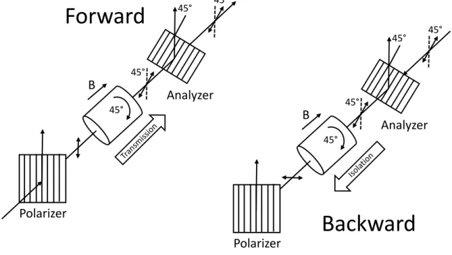
rotator, the polarization plane of the backward light is rotated by 45 degrees in the same direction as the first round. Therefore, this light is completely shut out by the polarizer because its polarization plane is now 90 degrees away from the light transmission axis of the polarizer. The performance of optical isolators is primarily evaluated by their insertion losses and isolation ratio (the ratio of the optical power propagating backward at the input to the forward power at the output), both of which are determined by the absorption losses end-face reflectance and the extinction ratios of optical elements.
Figure 1.1 Operation principle of a bulk-type optical isolator. 1.2.1.2 Polarization-independent type
While polarization-dependent optical isolators operate for the light polarized, only in a specific direction, polarization-independent isolators operate for any kind of polarization state. Consequently, these isolators are frequently used in optical fiber amplifiers. The basic working principle of a polarization-independent optical isolator was first proposed by T. Matsumoto [26]. Its arrangement consists of a Faraday rotator and a half-wave plate inserted between a pair of birefringent crystal plates of equal thickness (as spatial walk-off polarizer, SWP). The birefringent plate functions to split the incident beam into a pair of orthogonal rays and separate one ray ("E" ray) from the other ray ("O" ray) as they travel through the plate. This phenomenon of spatial displacement is often referred to as "walk off". The two separated components are rotated as they pass through the half-wave plate and the Faraday
rotator, and then enter the second birefringent plate where they are recombined to form the output signal. Since a Faraday rotator is a nonreciprocal device, any signal traveling in the reverse direction through the isolator will be physically separated into orthogonally polarized signals as it passes through both birefringent plates and will not be recombined into the input fiber. In an alternative design, a wedge-shaped spatial walk-off polarizer was used to bring a large separation of two polarization states in backward direction by Shirasaki. The schematic and working principle is depicted in figure 1.2.
Figure 1.2 The diagram of fiber-embedded polarization-independent isolator
1.2.2 Waveguide optical isolator
The bulk isolator is not suitable for integrating with other optical devices. Waveguide optical isolators have been investigated to realize the integrated circuit. There are a few basic concepts to construct the waveguide optical isolator. They utilize a mode conversion which corresponds to the Faraday rotation in a bulk isolator, an optical nonreciprocal phase shift which occurs in transverse magnetic (TM) modes, and a mode coupling between guided and radiation modes.
A mode-conversion type optical isolator consists of three parts that include input polarizer, Faraday rotator, and output polarizer. The Faraday rotator composes of a magnetic garnet such as yttrium iron
SWP Rotator λ/2 plate SWP D D (Side view) Fiber Fiber Fiber Fiber
Forward (end view)
Fiber Fiber
garnet and terbium gallium garnet, which have large Faraday rotation coefficient, placed in a cylindrical permanent magnet and rotates the polarization of passing light by 45 degrees. In forward direction, the light will propagate passing input polarizer and the polarized light will have only one direction (vertical plane). Then, the light passes through the Faraday rotation, so that the plane of polarization will be rotated 45 degrees. The output polarizer, which is aligned 45 degrees relating to the input polarizer, will then let the light pass through. On the other hand, light traveling in the reverse direction (backward direction) will pass through the output polarizer and become polarized by 45 degrees. The light passes through the Faraday rotator and experiences additional 45 degrees of non-reciprocal rotation. The light is now polarized in the horizontal plane and will be rejected by the input polarizer, which allows light polarized in the vertical plane to pass through. Owing to this principle, the device acts as a bulk-type optical isolator.
H
0 45oMagneto-optic rotation
Optically active rotation
Forward traveling wave
Backward traveling wave
H
0 45oMagneto-optic rotation
Optically active rotation
Figure 1.3 Operation principle of an optical isolator with parallel polarizers.
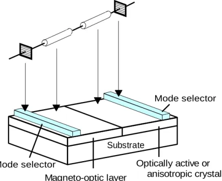
Substrate Mode selector Magneto-optic layer Optically active or anisotropic crystal Mode selector
Figure 1.5 The diagram of mode-conversion isolator.
Another type of the waveguide-type isolator is a “semileaky isolator”. An anisotropy was realized within refractive indices that were higher or lower than the garnet waveguide in order to obtain “semi-leaky” waveguides [29]. Figure 1.6 shows the basic geometry of the semileaky optical isolator. The nonreciprocal magneto-optic mode conversion was designed to be equal but opposite in the forward direction, then TE mode would experience little loss. On the other hand, in the backward direction, TM modes were generated and leaked away due to the higher cladding index. Due to the problem in an optical contact between the magneto-optic guiding layer and anisotropic superstrate, it is very difficult to fabricate this isolator [30].
GGG Substrate
Magneto-optic layer
LiNbO
3Input prism
Output prism
Figure 1.6 Basic geometry of the semileaky optical isolator.
q
mM
M
Substrate
Magneto-optic layer
Mode selector
An optical isolator employing a nonreciprocal phase shift is attractive because there is no need for phase matching or complicated control of the direction of magnetization [31]. The nonreciprocal phase shift occurs in TM modes travelling in magneto-optic waveguides, in which the magnetization is aligned transversely to the light propagation direction in the film plane. When a magneto-optic layer is used as a cladding layer in the magneto-optic waveguide, the nonreciprocal phase shift has its maximum with a high-refractive-index guiding layer [32].
An optical isolator based on a nonreciprocal guided-radiation mode conversion is realized [33-35]. The isolator operates on the basis of the nonreciprocal guided-radiation mode conversion in a channel waveguide. The optical isolator employing the nonreciprocal guided-radiation mode conversion is very attractive because of its simple structure. A backward TM mode is converted to TE radiation mode while a forward TM mode propagates with no mode conversion by arranging the propagation constant relationship of the two modes. It can be accomplished by the optical nonreciprocal phase shift which occurs in TM modes [36,37].
1.2.3 Optical circulator
Another type of passive element that is commonly used in fiber optic systems is the optical circulator [23,38]. An optical circulator is a special fiber-optic component that can be used to separate optical signals that travel in opposite directions in an optical fiber. It can be made with any number of ports. Moreover, if it makes sure the last port does not circulate around the first, the device can be used in systems where this feature is not required. The optical circulators are very versatile devices and may be used in many applications.
Figure 1.7 Behavior of an optical circulator.
1.3 Si photonics
For the global market of Si photonics, the Si photonics market is estimated to be USD 774.1 million in 2018 and is expected to USD 2.61 billion in 2024 that means the compound annual growth rate (CAGR) is growing up to 22.45%. This market is reported base on the product, applications, components, and regions. The Si photonics is produced for a transceiver, a switch, a variable optical attenuator, a cable, and a sensor. The Si photonics is realized in the application such as data center, telecommunications, military and defense, medical and life sciences, and sensing. The Si photonics is a perfect solution for high-density photonic integration, allowing the incorporation of photonic devices on a Si wafer. The problem to transfer huge data should be resolved through high-density photonic integration with photonics devices.
Si photonics means the implementation of some level of photonic integrated circuit in Si. The emergence of photonics and electronics based on a Si platform creates an ideal solution for optoelectronic integrated circuit which potentially enables optical interconnects with power consumption [40]. More than a decade’s researches, Si-based photonic devices are rapidly increasing their performances. Si-based micro and nano-waveguide devices have shown a lot of advantages, including high speed [41], low optical loss [42], low power consumption [43], small size [44], monolithic optoelectronic integrations [45], and hybrid material integration capability [46]. Si photonics has been developed as an integration technology that supports a wide range of compact photonic device on an integrated circuit for applications ranging from communication to sensing. Si photonics is employed in the project of HELIOS, PLATON, ePIXnet, iPHOS, RAMPLAS, PARADIGM, etc. [47]
Port 2
Port 3 Port 1
For example, HELIOS proposes to integrate Si photonic components with integrated circuits. HELIOS intends to realize a design and fabrication chain for integrating the photonic layer with CMOS circuit by using microelectronic fabrication processes. [48] HELIOS aims to develop a generic integration and manufacturing technology for high density and high-performance components and circuits involving passive and active photonic functions.
PLATON [49, 50] purposes to develop and demonstrate on-chip Tb/s optical router for back-plane or blade-server interconnects through merging plasmonics and silicon photonics technology, employing plasmonics for the switching functionalities and silicon photonics for filtering, multiplexing, and header detection processes. PLATON includes a router-chip with integrated photonics, plasmonics, and microelectronic components. PLATON aims to reduce the size and power consumption bottleneck in data center and high-performance computing system by realizing chip-scale high-throughput routing fabric with reduced energy consumption and footprint requirement. PLATON’s optical board technology is used to blend the functionally potential small-footprint, high-bandwidth plasmonic structures and the potential integration of plasmonics with the more mature silicon-on-insulator (SOI) technology providing a new generation of miniaturized photonic components.
Si is used as an optical medium and in complementary metal-oxide semiconductor fabrication processing technology. It allows tighter monolithic integration of many optical functions with a single device. Optical waveguides, modulators, and photo-detectors can be integrated within a single device, thus providing a smaller form factor. Many existing devices still require external laser sources and, therefore, light coupling capabilities at the input and output of a Si photonics IC are critical to the success of the product. There are still numerous challenges designers need to overcome in order to make Si photonics devices viable for mass adoption and the technology of choice for future optoelectronic communication. In 2015, Si photonics fundamentals were presented, the basic building blocks covering both active and passive elements, and discuss the contrast with existing multimode/single mode optoelectronics technology. It will provide an overview of the challenges which designers have already conquered to bring this technology to a stage where successful products are demonstrated.
smaller than those in the silica-based system; however, on a Si substrate it is very difficult to grow epitaxially the high-quality III–V materials needed for the construction of practical photonic devices.
Moreover, Si waveguides, such as rib-type waveguides with core dimensions of a few micrometers [51] and photonic wire waveguides with core dimensions of several hundreds of nanometers [52–54], are considered. The waveguide must have features that allow accommodating passive and dynamic photonic devices such as wavelength filters and modulators. The waveguide system must be flexible enough to allow active functions, such as light emission and detection to be implemented. A Si-based waveguide is obviously preferable for electronic photonic convergence.
1.4 Waveguide optical isolator for Si photonics
As for the communication network, the fiber optic supports the coming multimedia based society. This system is indispensable for transmitting audio data, as has been conventionally performed, in addition to transmitting large-volume data such as move data freely. The reflection of the bifurcation of optical fiber causes amplifier or laser diode failure, it has become a problem alongside the widening of services. Recently, branch connection systems for high-speed transmission or for a large number of subscribers, various other optical parts are required in addition to these core parts. These include optical amplifiers, splitters, optical isolators, optical couplers, optical branching filters, optical switches, optical modulators, optical attenuators, etc. Generally, the laser diode of the optical transmitter is built in the laser diode module integrated with optical parts such asthe optical fiber. The optical isolator is located between the laser diode and the optical fiber and prevents the penetration of reflected light to the laser diode.
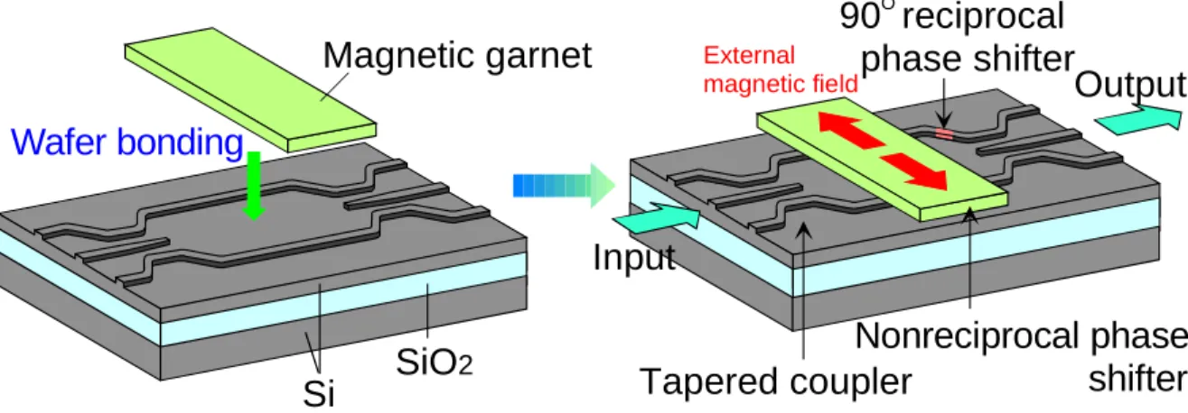
operated on the magneto-optic phenomenon of a nonreciprocal phase shift, rather that polarization conversion as for Faraday rotation based isolators [56]. As for MZI structure, there are complex waveguides. These structures need to apply the external magnetic field in two directions for isolator operation.
Magnetic garnet
Si
Wafer bonding
Tapered coupler
Output
External magnetic field90 reciprocal
phase shifter
OSiO
2Input
Nonreciprocal phase
shifter
Figure 1.8 The schematic drawing of SOI waveguide MZI optical isolator.
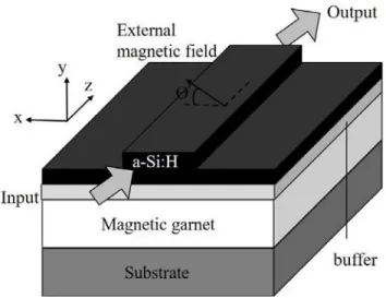
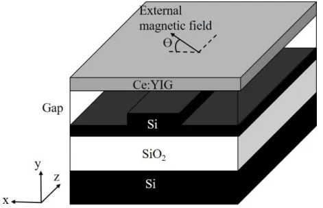
At the present, the author proposes rib-type optical isolators with the Si guiding layer. The rib-type waveguide is a simple structure. The external magnetic field is applied in these structure in one direction for isolator operation. The magneto-optic waveguide on the SOI substrate can be fabricated by bonding technique [57,58]. In the magneto-optic waveguide, the Si guiding layer is deposited on the SiO2 as
shown in figure 1.9. In this research, the author focuses on surface activated bonding and photosensitive adhesive bonding since they are suitable for bonding between Si and magnetic garnet at low temperature.
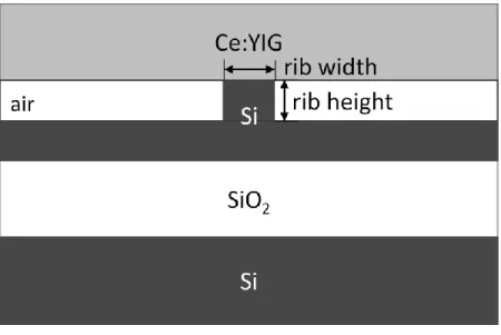
H. Yokoi et al. have proposed an optical isolator with a Si guiding layer deposited on a magnetic garnet layer [59]. Recently, an amorphous Si has attracted attention for integrated optics because of its low absorption loss and high refractive index [60-62]. In this thesis, the optical isolator with a hydrogenated amorphous Si (a-Si:H) guiding layer deposited on a garnet substrate is considered. The optical isolator with an a-Si:H guiding layer is shown in figure 1.10. The optical isolator employing the nonreciprocal guided-radiation mode conversion is designed. The principle of the nonreciprocal phase shift will be explained in the next chapter.
Figure 1.10 Optical isolator with hydrogenated amorphous Si (a-Si:H) guiding layer deposited on a magnetic garnet cladding layer.
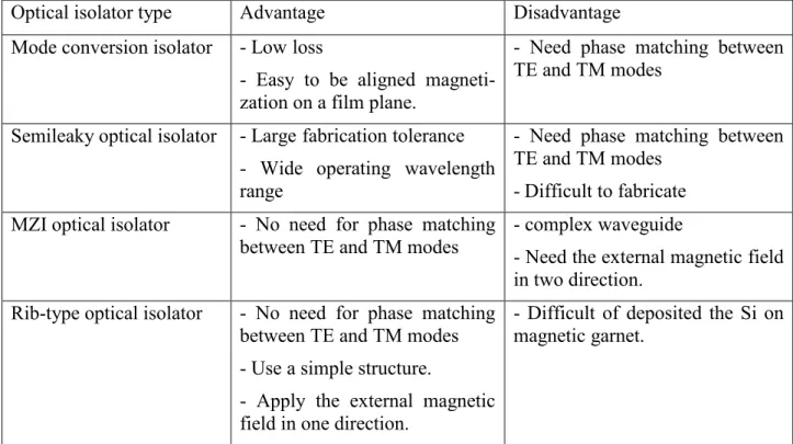
Table 1.1 The advantages and disadvantages of the magneto-optic waveguide for optical isolators.
Optical isolator type Advantage Disadvantage
Mode conversion isolator - Low loss
- Easy to be aligned magneti-zation on a film plane.
- Need phase matching between TE and TM modes
Semileaky optical isolator - Large fabrication tolerance - Wide operating wavelength range
- Need phase matching between TE and TM modes
- Difficult to fabricate MZI optical isolator - No need for phase matching
between TE and TM modes - complex waveguide - Need the external magnetic field in two direction.
Rib-type optical isolator - No need for phase matching between TE and TM modes - Use a simple structure.
- Apply the external magnetic field in one direction.
- Difficult of deposited the Si on magnetic garnet.
1.5 Organization of the dissertation
The optical fiber communication is used to transmit light and information over long distances. The optical isolator is indispensable in protecting optical active devices from unwanted reflected light. The waveguide optical isolator is desired in order to realize a photonic integrated circuit. In the near-infrared region, magnetic garnet crystals are necessary components for an optical nonreciprocal device because of their transparency and strong magneto-optic effect. Developing Si photonics technology, optical isolators with the Si guiding layer are desired.
This dissertation is composed of six chapters.
In chapter 2 “theories”, this chapter will explain propagation of light wave in the waveguide. The properties of garnet materials for optical isolators will be clarified. The magneto-optic effect is classified in Faraday effect, Cotton-Mouton effect, and Kerr effect. The calculation of the nonreciprocal phase shift will be described by solving the Maxwell equation. Moreover, the theory of fabrication process of magneto-optic waveguides is also illustrated such as surface activated bonding, photosensitive adhesive bonding, plasma-enhanced chemical vapor deposition (PECVD), spin coating, electron beam lithography (EBL), ultraviolet lithography, and etching.
In chapter 3 “magneto-optic waveguides fabricated by bonding technique”, the optical isolator employing the nonreciprocal phase shift is designed. An optical isolator constructed on a SOI substrate, a widely adopted substrate for modern optical devices is explained. The magneto-optic waveguide on the SOI substrate can be fabricated by bonding technique. An optical isolator employing a nonreciprocal guided-radiation mode conversion consists of a rib-type magneto-optic waveguide with a Si guiding layer. The optical isolator employing the nonreciprocal guided-radiation mode conversion is realized by calculating the isolation ratio. The electric field of TM guided mode and TE radiation mode are studied. Design of the optical isolator fabricated by surface activated bonding or photosensitive adhesive bonding is considered. Relationship of waveguide parameters for isolator operation is clarified for various gaps. In chapter 4 “magneto-optic waveguides with a-Si:H guiding layer”, an optical isolator with the amorphous Si guiding layer on a garnet substrate is investigated. The relationship of rib height and rib width for the isolator operation is clarified. The optical isolator employing the nonreciprocal guided-radiation mode conversion is realized by calculating the isolation ratio. The electric field of TM guided mode and TE radiation mode are studied. The magneto-optic waveguide with the a-Si:H guiding layer is fabricated and evaluated.
In chapter 5 “athermal operation of optical isolator”, the temperature dependence of the optical isolator is investigated. The relationship of rib height and rib width for the isolator operation is clarified for various operating temperatures. Refractive indices of layers in a magneto-optic waveguide are considered to circumvent the deviation of the waveguide parameters for isolator operation due to the temperature shift.
References
[1] T. H. Maiman, 1960, “Optical and Microwave-Optical Experiments in Ruby,” Phys. Rev. Letters, Vol. 4, No. 11, pp.564-566.
[2] https://lemelson.mit.edu/resources/robert-hall
[3] I. Hayashi, M. B. Panish, P. W. Foy, and S. Sunski, 1970, “Junction Lasers Which Operate Continuously
at Room Temperature,” Appl. Phys. Lett. 17, p. 109.
[4] K. Mettler, 1987, “Design and Performance of High Power Semiconductor Lasers,” Solid State Device Research Conference, European, pp. 817-825.
[5] F. S. Choa, T. L. Koch, U. Koren, and B. I. Miller, 1989, “Optoelectronic Properties of InGaAs/InGaAsP
Multiplr-quantum-well Waveguide Detectors,” IEEE photon. Technol. Lett., Vol. 1, pp. 376-378.
[6] K. C. Kao, and G. A. Hockham, 1966, “Dielectric-fibre surface waveguides for optical frequencies,” IEEE Proc. Vol. 113, pp. 1151-1158.
[7] F. P. Kapron, D.B. Keck, and R. D. Maurer, 1970, “Radiation Losses in Glass Optical Waveguides,” Appl. Pyhs. Lett., Vol. 17, p.423.
[8] R. G. Smith, 1972, “Optical Power Handling Capacity of Low Loss Optical Fibers as Determined by
Stimulated Raman and Brillouin Scattering,” Appl. Opt., Vol. 11, No. 11, pp. 2489-2494.
[9] S. E. Miller, 1969, “Integrated optics: An Introduction,” Bell Syst. Tech. J., Vol. 48, p. 2059.
[10] W. S. C. Chang, M. W. Muller, and F. J. Rosenbaum, 1974, “Integrated Optics,” Laser Appl. (Academic, New York), Vol. 2, p.1867.
[11] H. Kogelnik, 1975, “An Introduction to Integrated Optics,” IEEE Trans. Microwave Theory Tech., Vol. 23, p. 2.
[12] Y. Suematsu, 1975, “The progress of Integrated Optics in Japan,” IEEE Trans, Microwave Theory Tech., Vol. 23, p. 16.91978
[13] C. P. Lee, S. Margalit, I. Ury, and A. Yariv, 1978, “Integration of an injection laser with a Gunn oscillator
on a semi-insulating GaAs substrate,” Appl. Phys. Lett., Vol. 32, pp. 806-807.
[14] J. J. Hsieh, 1976, “Room- temperature Operation of GaInAsP/InP Double Heterostructure Diode
[15] T. L. Koch., F. S, Choa, U. Koren, R. P. Gnall, F. Hemandez-Gill, C. A. Burrus, M. G. Young, M. Oron, and B. I. Miller, 1990, “Balanced operation of a GaInAs/GaInAsP multiple-quantum-well integrated
heterodyne receiver,” IEEE Photon. Tech. Lett., Vol. 2, pp. 577-581.
[16] R. Lang, and K. Kobayashi, 1980, “External Optical Feedback Effects on Semiconductor Injection Laser
Properties,” IEEE J. of Quantum., Vol. QE-16, pp. 347-355.
[17] Y.-T. Sheen, 2007, “An Analysis Method for the Vibration Signal with Amplitude Modulation in a
Bearing System,” J. of Sound and Vibration, Vol. 303, pp. 538-552.
[18] H. Fukui, K. Furuya, and Y. Suematsu, 1987, “Suppression of mode hopping noise caused by external
reflaction in dynamic single mode (DSM) laser,” Trans. IEICEv Vol. E70, No. 7, pp. 857-864.
[19] K. Ikeda, and O. Akimoto, 1982, “Instability leading to periodic and chaotic self-pulsatations in a
bistable optical cavity,” Phys. Rev. Lett., Vol. 48, pp. 617-620.
[20] S. Yanase, R. N. Mondal, Y. Kaga, and K. Yamamoto, 2005, “Transition from Steady to Chaotic States
of Isothermal and Non-isotermal Flows through a Curved Rectangular Duct,” J. of the Physical Society
of Japan, Vol. 74, No. 1, pp. 345-358.
[21] D. Lenstra, B. H. Verbeek, and A. J. den Boef, 1985, “Coherence collapse in single-mode semiconductor
lasers due to optical feedback,” IEEE J. Quant. Electron., Vol. OE-21, pp. 674-679.
[22] Ki Young Kim, 2010, “Advances in Optical Photonic Devices,” 1st ed., In Tech, Shanghai, China, pp.117
- 135.
[23] http://www.fiber-optic-equipment.com/the-working-principle-of-the-optical-circulator.html.
[24] K. Chang, and W. Sorin, 1990, “High-performance single-mode fiber polarization-independent
isolators,” Opt. Lett., Vol. 15, Issue 8, pp. 449 - 451.
[25] K. Nakajima, Y. Numajiri, and Y. Nomi, 1991, “New design of a polarization-independent optical isolator
with high performance,” IEEE Trans. Magn., Vol. 27, Issue 6, pp. 5399 -5401.
[26] T. Matsumoto, 1979, "Polarization-Independent Isolators for Fiber Optics," Trans. IECE Japan, E62, pp.
516-517.
[27] J. P. Castera, and G. Hepner, 1997, “Isolator in integrated optics using the Faraday and Cotton-Mouton effects,” IEEE Trans. Magn. MAG-13, pp. 1583-1585.
[29] S. T. Kirsch, W. A. Biolsi, S. L. Blank, P. K. Tien, R. J. Martin, P. M. Bridenbaugh, and P. Grabbe, 1981, “Semi-leaky thin film optical isolator,” J. Appl. Phys., Vol. 52, no. 5, pp. 3190 -3199.
[30] S. Yamamoto, Y. Okamura, and T. Makimoto, 1976, “Analysis and design of semileaky-type thin-film optical waveguide isolator,” IEEE J. Quantum Electron., Vol. QE-12, pp. 764-770.
[31] H. Yokoi, T. Mizumoto, T. Takano, and N. Shinji, 1990, “Demonstration of an optical isolator by use of
a nonreciprocal phase shift,” Appl. Opt., Vol. 38, pp. 7409-7413.
[32] H. Yokoi, 2008, “Calculation of nonreciprocal phase shift in magneto-optic waveguides with Ce: YIG layer,” Opt. Mater., Vol. 31, pp. 189-192.
[33] T. Shintaku and T. Uno, 1994, “Optical waveguide isolator based on non- reciprocal radiation,” J. Appl.
Phys. Vol 76, no. 12, pp. 8155 - 8159.
[34] T. Shintaku, 1995, “Integrated optical isolator based on nonreciprocal higher- order mode conversion,”
Appl. Phys. Lett. Vol. 66, no. 21, pp. 2789 - 2791.
[35] T. Shintaku, 1998, “Integrated optical isolator based on efficient nonreciprocal radiation monde conversion,” Appl. Phys. Lett. Vol. 73, no. 14, pp. 1946 - 1948.
[36] S. Yamamoto, and T. Makimoto, 1974, “Circuit theory for a class of anisotropic and gyrotropic thin-film optical waveguides and design of nonreciprocal devices for integrated optics,” J. Appl. Phys., Vol.
45, pp. 882-888.
[37] F. Auracher, and H. H. Witte, 1975, “A new design for an integrated optical isolator,” Optics Commun.,
Vol. 13, pp. 435-438.
[38] http://www.fiberopticshare.com/passive -optical-components-optical-circulator.html. [39] F.-H. Hsu, J.-H. Chen, K.-H. Chen, C.-H. Yeh, and K. Y. Hsu, 2014, “Optimized design of multiport
optical circulator,” Optik, Vol. 125, pp. 2454-2457.
[40] D. A. B. Miller, 2009, “Device requirements for optical interconnects to silicon chip,” Proc. IEEE, Vol.
97, pp. 1166-1185.
[41] L. Vivien, A. Polzer, D. Marris-Morini, M. Hartmann, P. Croza, E. Cassan, C. Baudot, F. Boeuf, and J.-M. Fedeli, 2013, “40 Gbit/s germanium waveguide photodiode,” Opt. Express, Vol. 20, pp. 1096-1101.
[43] W. A. Zortman, A. L. Lentine, D. C. Trootter, and M. R. Watts, 2011, “Low-voltage differentially-signaled modulators,”, Opt Express, Vol.19, pp. 26017-26026.
[44] Q. Xu, D. Fattal, R. G. Beausoleil, 2008, “Silicon microring resonators with 1.5-µm radius,” Opt. Express,
Vol. 16, pp.4309-4315.
[45] C. Gunn, 2006, “CMOS photonics for high-speed interconnects,” IEEE Micro., Vol. 26, pp. 58-66.
[46] D. Liang, G. Roelkens, R. Baets, and J. E. Bowers, 2010, “Hybrid Integrated Platforms for Silicon Photonics,” Materials, Vol. 3, pp. 1782-1802.
[47] http://www.semicontaiwan.org/en/sites/semicontaiwan.org/files/data16/docs/(7)%20SEMICON%20Tai
wan%202016_Tekin_05.pdf.
[48] J. M. Fedeli, L. Di Cioccio, D. Marris-Morini, L. Vivien, R. Orobtchouk, P. Rojo-Romeo, C. Seassal, and F. Mandorlo, 2008, “Development of Silicon Photonics Devices Using Microelectronic Tools for the Integration on Top of a CMOS Wafer,” Advances in Opt. Tech. AOT, special issue: Silicon Photonics, Article ID 412518.
[49] S. Papaioannou, K. Vyrsokinos, D. Kalavrouziotis, G. Giannoulis, D. Apostolopoulos, H. Avramopoulos, F. Zacharatos, K. Hassan, J. – C. Weeber, L. Markey, A. Dereux, A. Kumar, S. I. Bozhevolnyi, A. Suna, O. G. de Villasante, T. Tekin, M. Waldow, O. Tsilipakos, A. Pitilakis, E. E. Kriezis, and N. Pleros, 2012, “Merging Plasmonics and Silicon Photonics Towards Greener and Faster “Network-on-Chip” Solutions for Data Centers and High-Performance Computing Systems,” INTECH, chap. 21, pp. 523-548.
[50] M. Humer, R. Guider, W. Jantsch, and T. Fromherz, 2013, “Integration, photostability and spontaneous emission rate enhancement of colloidal PbS nanocrystals for Si-based photonics at telecom wavelengths,” OSA. Ppt. Express, Vol. 21, No. 16, pp. 18680-18688.
[51] A.G. Rickman, G.T. Reed, and F. Namavar, 1994, “Silicon-on-insulator optical rib waveguide loss and
mode characteristics,” J. Lightwave Tech., Vol. 12, pp. 1771–1776.
[52] K. Yamada, T. Tsuchizawa, T. Watanabe, J. Takahashi, E. Tamechika, M. Takahashi, S. Uchiyama, H. Fukuda, T. Shoji, S. Itabashi, and H. Morita, 2004, “Microphotonics devices based on silicon wire waveguiding system,” IEICE Trans. Electron., Vol. E87-C, pp. 351–358.
[53] T. Tsuchizawa, K. Yamada, H. Fukuda, T. Watanabe, J. Takahashi, M. Takahashi, T. Shoji, E. Tamechika, S. Itabashi, and H. Morita, 2005, “Microphotonics devices based on silicon microfabrication technology,”
[54] P. Dumon, W. Bogaerts, V. Wiaux, J. Wouters, S. Beckx, J. V. Campenhout, D. Taillaert, B. Luyssaert, P. Bienstman, D. V. Thourhout, and R. Baets, 2004, “Low-loss SOI photonic wires and ring resonators fabricated with deep UV lithography,” Photon. Technol. Lett., Vol. 16, 1328–1330.
[55] H. Yokoi, T. Mizumoto, and Y. Shoji, 2003, “Optical nonreciprocal devices with a silicon guiding layer fabricated by wafer bonding,” Appl. Opt., Vol. 42, No. 33, pp. 6605-6612.
[56] Y. Shoji, I. W. Hsieh, R. M. Osgood, and T. Mizumoto, 2007, "Polarization-Independent Magneto-Optical Waveguide Isolator Using TM-Mode Nonreciprocal Phase Shift," J. Lightwave Technol. Vol. 25, pp.
3108 - 3113.
[57] T. Mizumoto, and Y. Shoji, 2014, “Optical Isolators and Circulators on Si Waveguide Platforms,” Int.
Conf. on Solid State Devices and Mater., pp. 502-503.
[58] C.-T. Ko, and K.-N. Chen, 2012, “Low Temperature bonding technology for 3D integration,” J.
Microelectron. Reliability, Vol. 52, Issue 2, pp. 302-311.
[59] H. Yokoi, K. Sasaki, and T. Aiba, 2009, “Sputter-deposited Si layer for optical isolator with Si guiding layer,” Jpn. J. Appl. Phys., Vol. 48, pp. 062202-1-062202-4.
[60] G. Cocorullo, F. G. D. Corte, R. De Rosa, I. Rendina, A. Rubino, and E. Terzini, 1998, “Amorphous silicon-based guided-wave passive and active devices for silicon integrated optoelectronics,” IEEE J. Sel. Top.
Quantum Electron., Vol. 4, No. 6, pp. 997-1002.
[61] A. Harke, T. Lipka, J. Amthor, O. Horn, M. Krause, and J. Miller, 2008, “Amorphous silicon 3-D tapers for Si photonic wires fabricated with shadow masks,” IEEE Photon. Tech. Lett., Vol. 20 pp. 1452-1454.
CHAPTER 2 THEORIES
2.1 Propagation of light wave
Light is a part of the electromagnetic spectrum, which is the collection of all waves such as visible light, microwaves, radio waves, and X-rays. In 1665, I. Newton [1,2] believed that light consists of a large number of minute material corpuscles emitted by a luminous body which produces the sensation of sight when these corpuscles strike the eye. The light travels with a tremendous speed in straight lines and homogeneous medium. This theory is used to explain the principle of rectilinear of light, laws of reflection as well as the law of refraction. A wavefront is a surface over which an optical wave has a constant phase. For example, a wavefront can be the surface over which the wave has a maximum or a minimum value. The shape of a wavefront is usually determined by the geometry of the source such as plane waves, cylindrical waves, and spherical waves. The direction of the wave propagation is always perpendicular to the surface of the wavefront at each point. However, the wavesfronts are produced by a point source in which they are concentric spheres in the principle.
In 1678, C. Huygens [3] considered the light waves propagation in longitudinal and explained the phenomenon of reflection, refraction, interference, and diffraction. When a wave travels in a single medium at a constant speed, the Huygen’s construction preserves the general form of the wavefront. That is, spheres propagate and become larger spheres, cylinders become larger cylinders, etc. If a portion of the wavefront enters a different medium, then the wavelets generated by each portion of the wavefront travel with the velocity that is appropriate for the medium that the wavefront locates. That is, the wavelets in the medium where the speed of light is lower will have smaller radii than the wavelets in the original medium. Michelson-Morley’s [4] experiment failed to detect the presence of ether, therefore, the ether concept was relinquished.
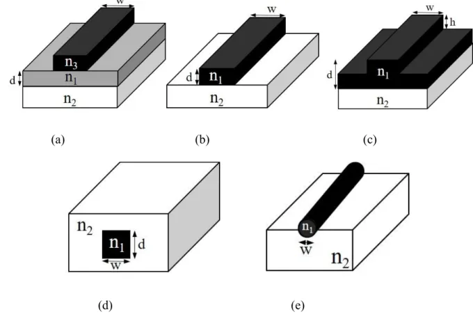
direction. The characteristics of a waveguide depend on the transverse direction profile of the refractive index n(x,y). There are two types of waveguide. First, it is a planar waveguide. There is an optical confinement in only one direction, the core is sandwiched between cladding layers in one direction. The core layer is called film, meanwhile the cladding layer is called cover and substrate, respectively. Second, it is a non-planar waveguide that is two dimensional transverse optical confinement. The core is covered by the cladding layer, and n(x,y) is a function of both x and y coordinates.
The optical waveguides are the important structure in semiconductor lasers used in order to control the light for various distance, and used in both passive and active devices. For waveguide, the index has abrupt changes between core and cladding that is called a step-index waveguide, meanwhile the index profile varying gradually is called a graded-index waveguide. Mostly, non-planar waveguides are used for device applications. The non-planar waveguides have a lot of types, that are differentiated by the distinctive feature of the index profiles. The waveguide types come from the group of non-planar waveguides, which include strip-loaded waveguides, ridge waveguides, rib waveguides, buried channel waveguides, and diffused waveguides as shown in figure 2.1(a)-(e).
(a) (b) (c)
(d) (e)
2.2 Garnet crystal
Garnets are some of the most magnetic gemstones. The most of all of the garnets acquire in the same properties and crystal forms, however, it has different chemical composition. Normally, the general formula of garnet is X3Y2(SiO4)3. The X site is usually occupied by divalent cations
(Ca, Mg, Fe, Mn) and the Y site by trivalent cations (Al, Fe, Cr) in an octahedral/ tetrahedral framework with SiO4 occupying the tetrahedral. Most gemologist garnets [5] are based on their color, refractive
index, and absorption spectrum [6-8]. Magnetic susceptibility measurements in conjunction with refractive index can be used to distinguish garnet species and varieties, and determine the composition of garnets in terms of percentages of end-member species within an individual gem.
The crystallographic structure of garnet has been expanded with the general formula X3Y2(ZO4)3.
For silicon, a large number of element has been instated of Z site including Ge, Ga, Al, V, and Fe [9]. Garnet films have large lattice parameters and thermal expansion mismatch with typical photonic substrates such as Si, GaAs, and InP. Good quality films are made by controlling the deposition and annealing processes. Yttrium iron garnet (YIG), the five iron(III) ions occupy two octahedral and three tetrahedral sites, with the yttrium(III) ions are coordinated by eight oxygen ions in an irregular cube. The iron ions in the two coordination sites exhibit different spins, resulting in magnetic behavior. YIG [10] is a versatile ceramic material with high melting point, large resistivity, high electromagnetic properties, etc. It is well-known as magnetic garnet and widely applied in electronics and microwave communication, such as in isolators, circulators, phase shifters, etc. In addition, Gadolinium Gallium Garnet (GGG) is synthesized for usage as a substrate for liquid-phase epitaxy of magnetic garnet films for bubble memory and magneto-optic applications. In this thesis, a cerium-substituted yttrium iron garnet (Ce:YIG) and calcium-, magnesium-, and zirconium-doped GGG ((Gd,Ca)3(Ga,Mg,Zr)5O12 or
GCGMZG) were considered.
3.2.1 Cerium-substituted yttrium iron garnet (Ce:YIG)
advantages such as well guided light, low magnetic field requirements, low cost, and the possibility of compact integration. YIG materials have been commercially used in microwave circuits like resonators, isolators, and circulators. There are many researches proposing the YIG waveguides because YIG has a Faraday rotation of several hundreds of deg/cm. Therefore, this order of length is needed for nonreciprocal polarization plane rotation. Large Faraday rotation materials are undesignable for compact integration, and Ce:YIG films have a large Faraday rotation as well. Gomi et al. [11] showed the giant Faraday rotation of Ce:YIG films which has been achieved by using radio frequency sputtering. They focus on the Faraday rotation spectrum and magnetic properties. Moreover, Ce:YIG films have been found to exhibit a large magneto-optic effect and low propagation loss. It will be good candidate material for devices with higher quality [11]. Tate et. al. [12] proposed the crystallinity of Ce:YIG iron garnet film prepared by radio frequency sputtering that was studied by using X-ray diffraction technique and transmission electron microscopy. Ce:YIG iron garnet films were synthesized by conventional radio frequency sputtering with ceramic target. The films were deposited on the substrates of gadolinium gallium garnet (GGG, lattice constant = 12.383Å) and GCGMZG (lattice constant = 12.496Å) [12], meanwhile the Ce:YIG lattice constant is approximately 12.57Å. Therefore, the optical characteristic of Ce:YIG thin films can be grown on the GCGMZG substrate completely.
3.2.2 Gadolinium calcium gallium magnesium zirconium garnet (GCGMZG)
3.3 Magneto-optic effect
The interaction of light is affected by the magnetic state of the medium and involves the electronic structure. The interaction between electromagnetic radiation and magnetically polarized materials results in magneto-optic effects. The important role of these effects of electromagnetism, providing an experimental support to the electromagnetic theory of light, as well as to both classical and quantum theory of matter including the motions of electron spin and spin-orbit coupling. The light is transverse electromagnetic wave which can be linearly, elliptically, or circularly polarized. A polarized light is included as a wave of electric field vector, oscillating along a given direction, and perpendicular to the propagation direction. The phenomena of magneto-optic effect can be explained by Faraday effect, Cotton-Mouton effect, and Kerr effect.
3.3.1 Faraday effect
M. Faraday [13] proposed the polarization of a linearly polarized light beam that is rotated upon propagating through a media which is placed in a magnetic field parallel to the propagation direction as shown in figure 2.2. The longitudinal magnetic field in the medium becomes optically active. The simple form of rotation (∅) is proportional to the strength of the magnetic field (B) and the length of the structure (l) as shown in Eq. 1.
∅ = 𝑉 ∫ 𝐵𝑑𝑙 = 𝑉𝑙𝐵0𝑙 (1)
V is noted as the Verdet constant that depends on the properties of medium, the ambient temperature,
and the wavelength of the incident light [14]. The angle of the rotation depends on the applied magnetic field. V is positive when the magnetic field is generated by positive current.
Figure 2.2 Operation principle of Faraday effect.
The electromagnetic wave in the medium are considered by Maxwell’s equation as follow:
∇.𝐷⃗⃗ = 0 (2) ∇.𝐵⃗ = 0 (3)
∇ × 𝐻′⃗⃗⃗⃗ = 1 𝑐 𝑑𝐷⃗⃗ 𝑑𝑡 (4) ∇ × 𝐸′⃗⃗⃗ = −1 𝑐 𝑑𝐵⃗ 𝑑𝑡 (5)
where 𝐷⃗⃗ is the electric displacement, 𝐵⃗ is the magnetic induction, 𝐻′⃗⃗⃗⃗ is the macroscopic magnetic field, and 𝐸′⃗⃗⃗ is the electric field. The electric displacement and the magnetic induction are related with the electric (𝜇 ) and magnetic (𝑚⃗⃗ ) moments. They are induced by the electromagnetic wave as follow:
𝐷⃗⃗ = 𝐸⃗ + 4𝜋 ∑ 𝑁𝑎 𝑎𝑚⃗⃗⃗⃗⃗⃗ 𝑎 (6) 𝐵⃗ = 𝐻⃗⃗ + 4𝜋 ∑ 𝑁𝑎𝜇⃗⃗⃗⃗ 𝑎
𝑎 (7)
where 𝑁𝑎 is the number of molecules per unit volume in state a. For the first component, the complex
induced moment vectors are shown:
𝑚𝑥= 𝛼𝑥𝑦𝐸′𝑦+ 𝛽𝑥𝑦𝐻′𝑦 (8) 𝜇𝑥 = 𝛾𝑥𝑦𝐸′𝑦+ 𝜒𝑥𝑦𝐻′𝑦 (9)
where 𝛼 and 𝜒 are the electric and magnetic polarizability tensors, respectively. There are also complex functions of the external magnetic field 𝐻⃗⃗ . The polarizability tensors can be explained:
𝛼𝑥𝑦 = 𝛼𝑥𝑦 (0) + 𝛼𝑥𝑦(1)𝐸𝑧+ ⋯ (10) 𝜒𝑥𝑦= 𝜒𝑥𝑦 (0) + 𝜒𝑥𝑦𝑧(1)𝐻𝑧+ ⋯ (11)
The electric and magnetic moments can be explained:
𝑚⃗⃗ = 𝛼(0)𝐸′⃗⃗⃗ + 𝛽(0)𝐻′⃗⃗⃗⃗ + 𝛼(1)(𝐸′⃗⃗⃗ 𝑥𝐻⃗⃗ ) + 𝛽(1)(𝐻′⃗⃗⃗⃗ 𝑥𝐻⃗⃗ ) (12) 𝜇 = 𝛾(0)𝐸′⃗⃗⃗ + 𝜒(0)𝐻′⃗⃗⃗⃗ + 𝛾(1)(𝐸′⃗⃗⃗ 𝑥𝐻⃗⃗ ) + 𝜒(1)(𝐻′⃗⃗⃗⃗ 𝑥𝐻⃗⃗ ) (13)
A complex index of refraction 𝑛̃± is solved by Maxwell’s equation: 𝑛̃ = 1 + 2𝜋 ∑ 𝑁± 𝑎{𝛼(0)𝑎 + 𝜒(0)𝑎∓ 𝑖𝛽
(0)𝑎 ± 𝑖𝛾(0)𝑎 [±𝑖𝛼(1)𝑎 + 𝑖𝜒(1)𝑎 + 𝛽(1)𝑎 − 𝛾(1)𝑎 ]𝐻𝑧}
𝑎 (14)
The Faraday rotation is described by this equation: 𝜙 = ω(𝑛̃ − 𝑛− ̃)/2𝑐+ . Therefore, the Faraday rotation can be written as follow: