Design and Measurement of the Silicon Slab Optical Waveguide
著者 ウィルダン パンジ トルスナ
著者別表示 WILDAN PANJI TRESNA journal or
publication title
博士論文本文Full 学位授与番号 13301甲第1923号
学位名 博士(工学)
学位授与年月日 2020‑09‑28
URL http://hdl.handle.net/2297/00061355
doi: https://doi.org/10.14710/jpa.v2i1.6421
Creative Commons : 表示 ‑ 非営利 ‑ 改変禁止 http://creativecommons.org/licenses/by‑nc‑nd/3.0/deed.ja
Dissertation
Design and Measurement of the Silicon Slab Optical Waveguide
シリコンスラブ光導波路の設計と測定
Graduated School of
Natural Science & Technology Kanazawa University
Division of Electrical Engineering &
Computer Science
Student ID. No. 1724042003 Name : Wildan Panji Tresna
Chief Advisor : Assoc. Prof. Takeo Maruyama
Date of Submission : January, 2020
ABSTRACT
The optical waveguide is one of the good supporting elements in the integrated circuits, because optical waveguide has brought advantages in terms of efficiency, energy consumption and size of the devices. The development of technology in the optical waveguide can be explored for many applications and purposes. Two of the most common types of optical waveguide are channel waveguide and optical slab waveguide. The quality factors of an optical waveguide are usually measured as propagation loss and scattering loss in the optical waveguide.
The silicon-based optical slab waveguide has been intensively studied at 1550 nm wavelength of light. The optical slab waveguide designed in our laboratory is built of silicon as a core, SiO
2as the bottom layer (substrate) and air as the top cladding layer respectively. In this case, the incident light will be confined and guided in silicon core region . Based on total internal reflection (TIR), we positioned a mirror at 45 degrees from horizontal parallel to light propagation. Furthermore, the effects of the mirror size, curvature radius, length of the slab waveguide and optimization of the coupling system are studied. The loss due to several components such as roughness and imperfectness of the design was comprehensively analyzed.
The effect of the mode propagation to the losses are also reviewed. According to
2
the experimental data on the TE mode propagation, the mirror loss on our slab
waveguide is 0.011 dB/mirror and the calculation on the TM mode is 0.007
dB/mirror. The mirror loss can indicate that there has been a slight loss on the mirror
which might have been caused by the imperfection of the design of a slab
waveguide.
3
ACKNOWLEDGMENTS
I would like to acknowledge my heartfelt gratitude to Assoc. Prof. Takeo Maruyama, for affording me the opportunity to pursue my education through join at High-Speed Laboratory (HS-Lab) as a doctor degree student. During the course, he always kindly supported and gave me invaluable advice on this research that made research progressing and going in the right direction. He also advises me not only the research but also mental attitude as a researcher, deeply analysis and some skill such us presentation technique, and so on. What make confident in my life.
Here, I would also like to thank all of students Lab member Motoharu Tanizawa, Hiroya Mitsuno, Takuma Ichikawa, Hirotaka Kato, Seiji Kamishima, Tetsuya Yoshida, Masato Shimada, Masataka Tsutsumi for your togetherness during my course especially for Alexander William Setiawan Putra who has been a good partner during course. Also thank you very much for intership student Nut and Mai from Thailand, Sun Bohan, Gao and Lu Shicheng from China.
Special thanks to Ministry of Research, Technology and Higher Education of
the Republic of Indonesia from the RisetPro scholarship which has given the
funding for me to continue my research in doctoral course program at Kanazawa
University.
4
Finally, I wish to particularly thank my beloved family for supporting and give
me comfort. Arista and my beloved children Zyva, Zuhayr and Zabyer for their
eternal patience and love. I am grateful to my parents, my young brother, for their
continuing support and encouraging me always try to take the giant steps in life.
5
List of figures
Figure 1. Propagation light on the three layers of the different material ………..22 Figure 2. The slab waveguide and channel waveguide on the side view ………….25 Figure 3. Beam profile on the three layers of the different material ……….………35 Figure 4. Normalized propagation constant dependence of the normalize frequency on TE
and TM mode ……….……….……….……….……….……….……….40
Figure 5. Gaussian beam propagation in free space ……….……….……….………45 Figure 6. A doubled lens collimates the output beam from a fiber ……….……….47 Figure 7. Cross section of a slab waveguide ……….……….……….……….………50 Figure 8. Cross section of a slab waveguide ……….……….……….……….………50 Figure 9. The taper design on the slab waveguide ……….……….……….………..52 Figure 10. Simulation result of the slab waveguide without and with the taper
design ……….……….……….……….……….……….……….……….….53
Figure 11. The taper design on the slab waveguide ……….……….……….………55
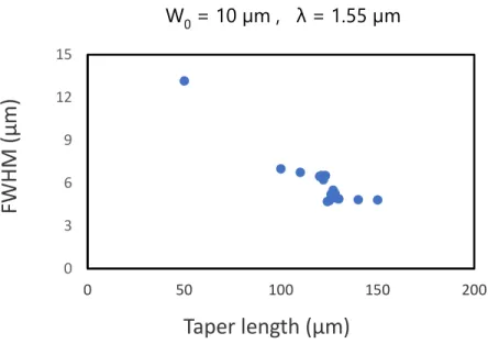
6 Figure 12. The dependence of FWHM on the taper length, FWHM is represent of the optical power on that position ……….……….……….……….……56 Figure 13. The mirror design on the slab waveguide. (a) flat mirror design, flat
design in 45o position. (b) curve mirror design has a certain radius ….58 Figure 14. The mirror design and simulation result on the slab waveguide. (a) flat
mirror design, (b) curve mirror design has a certain radius ……….…60 Figure 15. Simulation result of the curved mirror, power monitor ……….………62 Figure 16. The half-mirror design on the slab waveguide, the half-mirror consists
of the Si as the waveguide and SiO2 as the thin layer ……….………..64 Figure 17. The simulation result of the half-mirror design on the slab waveguide,
the incident light will be split after through the thin layer ……….……66 Figure 18. The simulation result of the half-mirror design on the slab waveguide,
the incident light will be split after through the thin layer ……….……67 Figure 19. The simulation result of the half-mirror design on the slab waveguide,
the transmitted and reflected power is strongly influenced by the
thickness ……….……….……….……….……….……….……….………69
7 Figure 20. The transmitted and reflected power dependence on the thickness of the half-mirror in the TE polarization ……….……….……….……….…….70 Figure 21. The transmitted and reflected power dependence on the thickness of the
half-mirror in the TM polarization ……….……….……….……….……72 Figure 22. The concept of the retroreflector in the slab waveguide ……….……….75 Figure 23. The concept of the integrated design in the slab waveguide ………….76 Figure 24. The simulation result of the integrated design, that design includes the taper design and the curved mirror design ……….……….……….……77 Figure 25. The concept of the integrated design in the slab waveguide, that design includes the taper design, the half-mirror design and the retroreflector
design ……….……….……….……….……….……….……….……….…78
Figure 26. The simulation result of the integrated design, that design includes the
taper design, half-mirror design and the retroreflector ……….……….79
Figure 27. The potentially loss in the slab waveguide system ……….……….……81
Figure 28. The experimental setup of the propagation loss measurement in the slab
waveguide ……….……….……….……….……….……….……….….…87
8 Figure 29. The measurement component in the input port and the output port ……90 Figure 30. The optical waveguide design consists of the channel waveguide, linear taper and slab waveguide ……….……….……….……….……….……...93 Figure 31. The dependence of total loss on the waveguide length in the slab
waveguide. “n” is the number of mirrors. and are the TE and TM polarizations, respectively ……….……….……….……….……….……95 Figure 32. The dependence of total loss after subtracted by the coupling on the
number of mirror ……….……….……….……….……….……….……97 Figure 33. The dependence of the mirror loss on number of mirrors in the slab
waveguide. “L” is the distance between mirrors, and are the TE and TM
polarizations, respectively ……….……….……….……….………100
Figure 34. The calculation of the average mirror loss in the slab waveguide ……102
9
TABLE OF CONTENTS
ABSTRACT
ACKNOWLE|DGEMNETS List of Figures
CHAPTER 1 Introduction
1.1. Motivation ………..……11
1.2. Objectives ………..….14
1.3. Thesis Organization ………....14
CHAPTER 2 Silicon Waveguide 2.1. Integrated Optics ………17
2.2. Introduction to wave guiding ………...19
2.3. Propagation in Theory ………21
2.3.1 Polarization ……….23
3.2.2 Mode in Waveguide ………23
2.4. Optical waveguide ………...25
2.4.1. Light propagation in free-space………...25
2.4.1.1 Maxwell equations ……….26
10
2.4.1.2 Boundary Condition ………...31
2.4.1.3 Optical Power ………..32
2.5 Slab waveguide ……….33
2.5.1 Wave equation ………...33
2.5.1.1 TE mode ………...34
2.5.1.2 TM mode ………..34
2.5.2 Dispersion equation ………...35
2.5.2.1 TE mode ………...36
2.5.2.2 TM mode ………..40
2.6 Finite Different Time Domain ……….43
2.7 Gaussian Beam & Beam Divergence ………44
2.7.1 Collimated beam ……….47
CHAPTER 3 Design and Simulation Result 3.4 Introduction ………49
3.1.1 Design and Simulation ……….49
3.5 Design and simulation result ………...51
3.2.2 Taper design ………...51
3.2.3 Mirror design ……….57
11
3.2.4 Half-mirror design ………..63
3.2.5 Retroreflector design ……….74
3.3 Integrated design ……..………76
3.4 Potentially loss on the system ………80
CHAPTER 4 Experimental Set up 4.1 Fabrication by Foundry service ………82
4.1.1 Fabrication flow ………84
4.2 Experimental set up for the propagation loss ………..85
CHAPTER 5 Result and Discussion 5.4 Experimental result ………94
5.1.1 Coupling loss ………..96
5.1.2 Waveguide loss ………98
5.1.3 Mirror loss ………..102
CHAPTER 5 Conclusion ………..105
REFERENCES ………..107
APPENDIX ………113
12
Chapter 1 Introduction
Current and future technological developments will be greatly influenced by the progress of integrated circuits, both in the electronic, optical or a combination of both. One thing that is very supportive in the development of integrated circuits is the optical waveguide, this is because the optical waveguide has brought increased efficiency, energy consumption and size of the device. The comparison between the development of circuits functionality and the cost per circuit becomes an interesting issue to discuss
Currently the development of optical waveguide can be enjoyed in a variety of applications and purposes, ranging from displays, storage to the field of security.
The two most prominent things about the types of optical waveguide that are widely
used are channel waveguide and slab or planar waveguide. The quality of an optical
waveguide is usually determined by propagation loss and scattering loss. But
because the optical waveguide will be connected to an emitter device such as a laser
13 or LED, there is usually loss due to connectivity, usually called coupling loss. As we all know that the waveguide channel has an advantage in confinement factor but the slab waveguide has other characteristics such as interference and scattering when two propagation lights do not intersect.
A planar waveguide allows light guiding through its volume without significant changes on its properties, thus opening the door to many high technology applications which include the communications, sensors, lasers and optics industrial sectors, among many others. Moreover, a number of new devices may be developed based on optical interconnects to implement distribution systems in parallel or cross-optical signals. The possibility of fabricating planar waveguides using inexpensive and simple technology opens a very interesting field of science.
In the optical slab waveguide, some references have discussed about how to
focus light propagation into a waveguide slab, which is by utilizing a fine
trapezoidal design which is commonly called a taper.
6-9)The tapered design also
can be applied in many applications in waveguides.
10-13)Beside the tapered design,
other application of slab waveguide that needs to be further developed is the mirror
design in slab waveguide. A mirror is usually constructed from differences of the
refractive index between the optical waveguide and mirror edge.
14 The silicon-based optical slab waveguide has been intensively studied at 1550 nm wavelength of light. The optical slab waveguide designed in our laboratory is built of silicon as a core, SiO
2as the bottom layer (substrate) and air as the top cladding layer respectively. In this case, the incident light will be confined and guided in silicon core region.
23-32)Based on the refractive index differences between the core, substrate and upper cladding, the mirror in the optical slab waveguide with a 45-degree angle is fabricated and analyzed the mirror loss.
33-36)However, inputting the light from the optical fiber into optical slab waveguide is difficult. It is also difficult to collimate this input light during propagation in slab waveguide. To solve these problems, the light propagation is introduced to the slab waveguide through additional taper waveguide to collimate the input light.
In this article, we propose to analyze some optical properties such us propagation
loss, coupling loss and the mirror loss for the transverse electric (TE) and transverse
magnetic (TM) modes. The characteristic of TE and TM modes when the light
source propagates to the waveguide will determine the quality of the waveguides.
15
1.1. Objective
The main objective of this research is to design, construct, and test by simulation for optical silicon slab waveguide. The design of the slab waveguide consists of the taper design, curve mirror design, half-mirror design and retro reflector design. however, the optical integration in slab waveguide has never been analyzed in detail. The purpose of this research is to measure and analyze in detail about an optical slab waveguide in terms of propagation loss and loss of mirrors. The waveguides must be characterized to know their guiding properties.
Furthermore, we also carry out simulations with the FDTD solution in the same design and compare the simulation with experimental results.
1.2. Thesis Organization
In this chapter for introduction, a historical review of the optical technology and developments is discussed at first. And then, as the background of this study, some kind of the optical waveguide such as channel and slab waveguide were argued for completing the application of the optical waveguide.
In the chapter 2, many design of the slab waveguide was realized. The design
included the taper, curve mirror, half-mirror design and retro-reflector design. All
16 of design was described completely, how to get the dimension of the design, hypothesis of the function on each design and also integrated two or three kind of the design on the slab waveguide.
In chapter 3, the characteristic of the slab waveguide was gotten by experiment.
The characteristic of the slab waveguide consists of the coupling loss, the waveguide loss and the mirror loss. Tunable Semiconductor Laser (TSL) used as a light source with the wavelength 1550 nm and 1mW as an output power. The experimental set up consists of the TSL, single mode fiber, then connected to the rotate wave plate. In the rotate wave plate there are Quarter Wave Plate (QWP) and Half Wave Plate (HWP), the combination between QWP and HWP produce one polarization, that is only TE or TM mode. The polarizing maintenance fiber (PMF) used to keep the output mode from the rotate wave plate, and then connected to the lens fiber to insert the power as much as possible.
In chapter 4, the experimental data and analysis of the propagation loss is
reported. In addition, we discuss the influenced of the waveguide length to the
propagation loss, also the influenced of the distance between mirrors and the
number of mirror to the mirror loss. The coupling loss is very influenced by the size
of the optical fiber in the input and output port.
17
In chapter 5, there will be brief summary of this study and give some future
works on this study.
18
Chapter 2
Silicon waveguide
2.1. Integrated Optics
The term “integrated photonics” refers to the fabrication and integration of several photonic components on a common planar substrate. These components include beam splitters, gratings, couplers, polarizers, interferometers, sources and detectors, among others.
The science that studies the light is called optics. It describes and studies the generation, as well as, the propagation of the light and its interaction with the matter.
Optics is an old science, but in the last century it has suffered a spectacular
renaissance. The first and more important development in modern optics, without
any doubt, was the invention of the laser by T.H. Maiman in 1960 [52]. The
development of semiconductor optical devices and the introduction of new
fabrication techniques for obtaining optical fibers with very low propagation losses
have been important. As a result of these new developments and associated with
19 other technologies, such as electronics, new disciplines such as electro-optics, opto- electronics, etc. have been generated.
Due to the combination of electronics and optics, new devices, more complex than lasers, semiconductor detectors, light modulators, etc. have appeared. Then a new scientific discipline has arisen to explain these new devices, which are not completely described for optics neither electronics. This scientific branch of applied physics is called photonics. If electronics can be considered as the discipline that describes the flow of electrons, the term of photonics deals with the control of photons.
In integrated photonics, the basic optical elements for generation, focusing, splitting, junction, etc. of light should be integrated in a single optical chip. Thus, the main goal purposed by integrated photonics is therefore the miniaturization of optical systems. This is possible thanks to the small wavelength of the light, which permits the fabrication of circuits and compact photonic devices with sizes of the order of microns.
The integration of passive and active optical devices, in a multicomponent circuit
is known as an integrated optic circuit (IOC). Integrated optic devices interface
20 efficiently with optical fibers, and can reduce the cost in complex circuits by eliminating the need for separate, individual packaging of each circuit element.
They also offer smaller size and weight, lower power consumption, improved reliability, and often larger electrical modulation bandwidth compared to their bulk- optic counterparts.
2.2. Introduction to wave guiding
The basic elements of silicon electronics are transistors and interconnects: the transistors perform logic operations, while the interconnects transfer digital information between these transistors. The performance of transistors has steadily been improved by the shrinking of their dimensions. Interconnect performance, however, does not typically get better when sizes are reduced. Electrical interconnects were improved in the past by changing the technology used to fabricate the wiring layers. The ultimate limitations of electrical interconnects have physical, not technological, origins, and these limits are rapidly approaching.
The use of optical links can be the way to avoid the problems of electrical
transmission. These optical interconnects are still the most promising candidate to
solve the challenges imposed by electrical wiring, both for off-chip and possibly
21 on-chip applications. [7] The band gap of silicon (~1.1 eV) is such that the material is transparent to wavelengths commonly used for optical transport (around 1.3–
1.6μm). One can use standard CMOS processing techniques to sculpt optical waveguides onto the silicon surface. Similar to an optical fiber, these optical waveguides can be used to confine and direct light as it passes through the silicon.
[9]
Due to the wavelengths typically used for optical transmission and silicon’s
high index of refraction, the feature sizes needed for processing these silicon
waveguides are on the order of 0.5 – 1 μm. SOI single -mode rib waveguides with
core dimensions comparable with single-mode optical fibers have previously been
demonstrated. In many cases, these large dimensions are needed because one uses
waveguides with a low refractive index contrast. By increasing this index contrast,
the confinement can be improved, but this also means that the waveguide core
should be reduced in size to keep the waveguide single mode. Then, however, the
geometrical features not only become very small but have to be very accurately
fabricated. [10]
22
2.3. Propagation in Theory
A very simple approach to describe the propagation of guided waves in a given medium is the optical ray model, which provides a good understanding of this propagation without having to handle with the solution to Maxwell’s equations. [9].
The basic law that this model uses to describe the behavior of propagating waves in the surface between two mediums (or interface) with different refractive indexes is Snell’s Law, which says that an incident field to this surface will be partly transmitted and partly reflected.:
n
1sinθ
1= n
2sinθ
2(2.1) being n
1and n
2the refractive indexes of the mediums, and θ
1and θ
2the angle of reflection and the angle of transmission, respectively.
It can be demonstrated from this law that angles smaller than a critical angle θc will experiment total internal reflection (TIR), which means that there is no transmitted field. This angle is given by the next expression:
𝑠𝑠𝑠𝑠𝑠𝑠 θ
𝑐𝑐=
𝑛𝑛𝑛𝑛21
(2.2)
This law applies also in the case of generic slab waveguides, like the one
depicted in Figure 2.1. It can be shown that the propagation in such a waveguide
will experiment total internal reflection in both interfaces.
23 Figure 1. Propagation light on the three layers of the different material
In general, n
1> n
2, n
3to ensure propagation by total internal reflection. In the case of n
2= n
3the waveguide is called symmetrical, and asymmetrical if not. In the following sections the basic characteristics of guided waves are described, which will be used to characterize and describe the behavior and performance of optical devices.
y n
2z
n
1n
3θ
1θ
124 2.3.1 Polarization
The fields that can propagate in a medium are normally classified in two possible polarizations: transverse electric (TE), when the electric field is perpendicular to the plane of incidence, or transverse magnetic (TM), when the magnetic field is perpendicular to the same plane. [9] TE and TM modes in an optical waveguide do not have a uniform linear polarization direction, so cannot be described as horizontal or vertical. In TE modes, the electric field vector is everywhere transverse and perpendicular to the waveguide axis. In TM modes, the magnetic field is the transverse. In a circular dielectric waveguide such as an optical waveguide, the electric field of the TM modes is largely radial with a small axial component, and the transverse magnetic field is circumferential. For TE modes, the magnetic field is radial, and the electric field direction circular. In both TE and TM modes, the transverse field components are zero at the center of the optical waveguide.
2.3.2 Mode in waveguide
However, light only propagates in a set of allowed discrete angles. The
equation that has to be solved (for TE modes) in a generic asymmetrical waveguide
is the following:
25 k
0𝑠𝑠
1ℎ cos 𝜃𝜃
1− 𝑚𝑚𝑚𝑚 = tan
−1�
sin2𝜃𝜃1−�𝑛𝑛2𝑛𝑛1�2cos 𝜃𝜃1
+ tan
−1�
sin2𝜃𝜃1−�𝑛𝑛3𝑛𝑛1�2cos 𝜃𝜃1
2.3
with 𝑘𝑘 =
2𝜆𝜆πthe propagation constant in free space and h the height of the core
layer. Every allowed angle gives place to a specific field, also called mode of
propagation, and is indicated by its mode number with the index m. The mode with
m = 0 is known as fundamental mode. For every interface the critical angle will be
different, so the angle that guarantees total internal reflection in both interfaces is
the one that gives solution to this equation (the larger). Single mode conditions can
be derived from this equation. Single mode waveguides do not suffer from
intermodal dispersion, which is the dispersion caused by the different velocities
with which every mode travels in the waveguide. In this way the shape of the
transmitted signal remains more similar after going through the waveguide. In
addition, if the waveguide is multimode, the total power transmitted has to be
shared by all the modes, and so the fundamental mode has lower power.
26
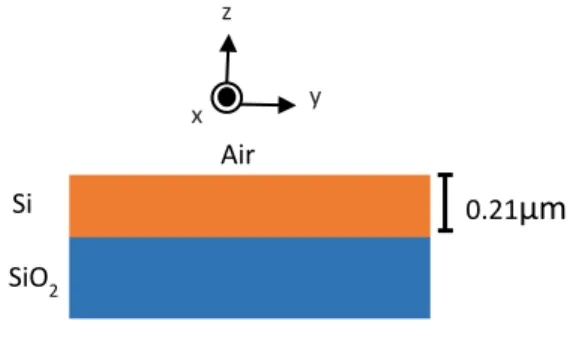
2.4. Optical Waveguide
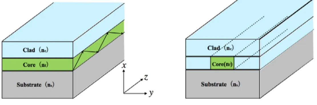
An optical waveguide is a basic waveguide for configuring an optical integrated circuit, a semiconductor laser, or the like, and generally has a structure in which a core having a square or rectangular cross section is surrounded by a clad having a lower refractive index. An example of the structure of an optical waveguide is shown in Fig. 2. In the Figure 2 (a) shows a slab optical waveguide, in this case, light is confined only in the x direction and propagates in the z direction. In contrast, in the channel optical waveguide shown in Fig. 2 (b), light is confined in the x and y directions and propagates in the z-direction.
Figure 2. The slab waveguide and channel waveguide on the side view
27
2.5. Maxwell Equation
Since light is an electromagnetic wave, it follows Maxwell's equation. Maxwell's equations describe how electric and magnetic fields are generated by charges, currents, and changes of the fields. An important consequence of the equations is that they demonstrate how fluctuating electric and magnetic fields propagate at a constant speed (c) in a vacuum . In the waveguide Maxwell's equations are shown below.
𝑑𝑑𝑠𝑠𝑑𝑑 𝐷𝐷 = 𝜌𝜌 (2.4)
𝑑𝑑𝑠𝑠𝑑𝑑 𝐵𝐵 = 0 (2.5) 𝑟𝑟𝑟𝑟𝑟𝑟 𝐸𝐸 = − 𝜕𝜕𝐵𝐵
𝜕𝜕𝑟𝑟 (2.6) 𝑟𝑟𝑟𝑟𝑟𝑟 𝐻𝐻 = 𝐽𝐽 + 𝜕𝜕𝐷𝐷
𝜕𝜕𝑟𝑟 (2.7)
Where E is the electric field, D is the electric flux density, H is the magnetic field, B is the magnetic flux density, ρ is the charge density, and J is the current density.
In general, the electric flux density D, magnetic flux density B, and current density
J can be expressed by the following equations.
28 𝐷𝐷 = 𝜀𝜀𝐸𝐸 = 𝜀𝜀
0𝜀𝜀
𝑆𝑆𝐸𝐸 (2.8) 𝐵𝐵 = 𝜇𝜇𝐻𝐻 = 𝜇𝜇
0𝜇𝜇
𝑆𝑆𝐻𝐻 (2.9)
𝐽𝐽 = 𝜎𝜎𝐸𝐸 (2.10)
Where ε is the dielectric constant of the medium, μ is the magnetic permeability of the medium, ε
sis the relative dielectric constant of the medium, μ
ris the relative magnetic permeability of the medium, σ is the conductivity, ε
0is the dielectric constant in vacuum, and μ
0is in the vacuum Is the magnetic permeability. About light waves
𝜇𝜇
𝑟𝑟= 1, 𝐽𝐽 = 0, 𝜌𝜌 = 0, 𝜎𝜎 = 0
Are often considered, and Maxwell's equations are given below.
𝑟𝑟𝑟𝑟𝑟𝑟 𝐸𝐸 = −𝜇𝜇
0𝜕𝜕𝐻𝐻
𝜕𝜕𝑟𝑟 (2.11) 𝑟𝑟𝑟𝑟𝑟𝑟 𝐻𝐻 = 𝜀𝜀 𝜕𝜕𝐸𝐸
𝜕𝜕𝑟𝑟 (2.12)
29 Consider the propagation of a plane wave expressed by the following equation.
𝐸𝐸 = 𝐸𝐸
(𝑥𝑥,𝑦𝑦)𝑒𝑒
𝑗𝑗(𝜔𝜔𝜔𝜔−𝛽𝛽𝛽𝛽)(2.13)
𝐻𝐻 = 𝐻𝐻
(𝑥𝑥,𝑦𝑦)𝑒𝑒
𝑗𝑗(𝜔𝜔𝜔𝜔−𝛽𝛽𝛽𝛽)(2.14)
Here, β is a propagation constant, and ω is the angular frequency of light.
Substituting the above equation into Maxwell's equations (2.11) and (2.12).
𝑟𝑟𝑟𝑟𝑟𝑟 𝐸𝐸 = −𝜇𝜇
0𝜕𝜕
𝜕𝜕𝑟𝑟 {𝐻𝐻
(𝑥𝑥,𝑦𝑦)𝑒𝑒
𝑗𝑗(𝜔𝜔𝜔𝜔−𝛽𝛽𝛽𝛽)} = −𝑗𝑗𝑗𝑗𝜇𝜇
0𝐻𝐻 (2.15) 𝑟𝑟𝑟𝑟𝑟𝑟 𝐻𝐻 = 𝜀𝜀 𝜕𝜕
𝜕𝜕𝑟𝑟 {𝐸𝐸
(𝑥𝑥,𝑦𝑦)𝑒𝑒
𝑗𝑗(𝜔𝜔𝜔𝜔−𝛽𝛽𝛽𝛽)} = 𝑗𝑗𝑗𝑗𝜀𝜀𝐸𝐸 (2.16)
When said formula is divided into each component, it is expressed by the following formula.
𝜕𝜕𝐸𝐸
𝛽𝛽𝜕𝜕𝜕𝜕 −
𝜕𝜕𝐸𝐸
𝑦𝑦𝜕𝜕𝜕𝜕 = −𝑗𝑗𝑗𝑗𝜇𝜇
0𝐻𝐻
𝑥𝑥(2.17)
𝜕𝜕𝐸𝐸
𝑥𝑥𝜕𝜕𝜕𝜕 −
𝜕𝜕𝐸𝐸
𝛽𝛽𝜕𝜕𝜕𝜕 = −𝑗𝑗𝑗𝑗𝜇𝜇
0𝐻𝐻
𝑦𝑦(2.18) 𝜕𝜕𝐸𝐸
𝑦𝑦𝜕𝜕𝜕𝜕 −
𝜕𝜕𝐸𝐸
𝑥𝑥𝜕𝜕𝜕𝜕 = −𝑗𝑗𝑗𝑗𝜇𝜇
0𝐻𝐻
𝛽𝛽(2.19)
𝜕𝜕𝐻𝐻
𝛽𝛽𝜕𝜕𝜕𝜕 −
𝜕𝜕𝐻𝐻
𝑦𝑦𝜕𝜕𝜕𝜕 = 𝑗𝑗𝑗𝑗𝜀𝜀𝐸𝐸
𝑥𝑥(2.20)
30 𝜕𝜕𝐻𝐻
𝑥𝑥𝜕𝜕𝜕𝜕 −
𝜕𝜕𝐻𝐻
𝛽𝛽𝜕𝜕𝜕𝜕 = 𝑗𝑗𝑗𝑗𝜀𝜀𝐸𝐸
𝑦𝑦(2.21)
𝜕𝜕𝐻𝐻
𝑦𝑦𝜕𝜕𝜕𝜕 −
𝜕𝜕𝐻𝐻
𝑥𝑥𝜕𝜕𝜕𝜕 = 𝑗𝑗𝑗𝑗𝜀𝜀𝐸𝐸
𝛽𝛽(2.22)
Consider a plane wave (one-dimensional wave) propagating in a homogeneous medium in the z direction. For plane waves, E and H are constant in any xy-plane, so
∂∂x
= 0 and
∂∂y
= 0 . Therefore, the plane waves propagating in the z direction from Eq. (2.19) and (2.22) are H
z= 0 and E
z= 0, and have no component in the propagation direction. It can also be divided into two equations: equations containing only E
xand H
y(Equations (2.18) and (2.20)) and equations containing only H
xand E
y(Equations (2.17) and (2.21)). This solves the equations for H
xand E
y. Partially differentiate equation (2.17) by z.
𝜕𝜕
2𝐸𝐸
𝑦𝑦𝜕𝜕𝜕𝜕
2= 𝑗𝑗𝑗𝑗𝜇𝜇
0𝜕𝜕𝐻𝐻
𝑥𝑥𝜕𝜕𝜕𝜕 (2.23)
Substitute equation (2.21) into equation (2.23).
𝜕𝜕
2𝐸𝐸
𝑦𝑦𝜕𝜕𝜕𝜕
2= 𝑗𝑗𝑗𝑗𝜇𝜇
0× 𝑗𝑗𝑗𝑗𝜀𝜀𝐸𝐸
𝑦𝑦= −𝑗𝑗
2𝜀𝜀𝜇𝜇
0𝐸𝐸
𝑦𝑦(2.24)
The solution of this wave equation is expressed by the following equation.
31 𝐸𝐸
𝑦𝑦= 𝐴𝐴𝑒𝑒
−𝑖𝑖𝜔𝜔�𝜀𝜀𝜇𝜇0 𝛽𝛽+ 𝐵𝐵𝑒𝑒
𝑖𝑖𝜔𝜔�𝜀𝜀𝜇𝜇0 𝛽𝛽(2.25)
The first term on the right side represents a wave traveling in the positive z-direction, and the second term represents a wave traveling in the negative z-direction.
Consider the case in a vacuum. Since ε = ε
0in a vacuum, ω �(𝜀𝜀𝜇𝜇
0) becomes ω �(𝜀𝜀
0𝜇𝜇
0) . The portion of ω �(𝜀𝜀
0𝜇𝜇
0) represents the phase rotation angle when moving 1 m in the z- direction, which is called wave number in vacuum, and is represented by k
0.
𝑘𝑘
0= 𝑗𝑗�𝜀𝜀
0𝜇𝜇
0(2.26)
Further, the wavelength in vacuum is represented by λ, and since it rotates 2π at one wavelength, the rotation angle per 1 m is represented by the following formula.
𝑘𝑘
0= 2𝑚𝑚
𝜆𝜆 (2.27) The following equation is obtained from equations (2.26) and (2.27).
1
�𝜀𝜀
0𝜇𝜇
0= 𝑓𝑓𝜆𝜆 = 𝑐𝑐 (2.28)
32 When c is the speed of light in vacuum, and c = 3 × 10
8m⁄s.
Next, consider the case of propagating through a medium with a refractive index of n. From the relationship of ε = ε
Sε
0and ε
S= n
2, 𝑗𝑗 �(𝜀𝜀𝜇𝜇
0) = 𝑗𝑗 �(𝜀𝜀
0𝜇𝜇
0) n = k
0n. Thus, the wave number of the plane wave propagating through the medium having the refractive index n is k
0n. Therefore, the speed of light is
1𝑛𝑛
in a medium having a refractive index n.
2.6 Boundary Condition
Consider a situation where two different media with ε
1, ε
2and permeability μ
1, μ
2are in contact. When the tangential component is placed on the boundary surface of the electromagnetic field in each medium as E
t1, E
t2, H
t1, H
t2, and the normal component is placed on the boundary surface as E
n1, E
n2, H
n1, H
n2, the electromagnetic field satisfies the following conditions.
�𝐸𝐸
𝜔𝜔1= 𝐸𝐸
𝜔𝜔2𝐻𝐻
𝜔𝜔1= 𝐻𝐻
𝜔𝜔2(2.29) � 𝜀𝜀
1𝐸𝐸
𝑛𝑛1= 𝜀𝜀
2𝐸𝐸
𝑛𝑛2𝜇𝜇
1𝐻𝐻
𝑛𝑛1= 𝜇𝜇
1𝐻𝐻
𝑛𝑛2(2.30)
33 That is the tangential components of the electric field and the magnetic field are continuous at the boundary surface of the medium, and the normal components of the electric flux density and the magnetic flux density are also continuous.
2.7 Optical Power
The pointing vector S representing the energy density of the electromagnetic field is defined by the following equation.
𝑆𝑆
(𝜔𝜔)= 𝐸𝐸
(𝜔𝜔)× 𝐻𝐻
(𝜔𝜔)(2.31)
Equation (2.31) is the instantaneous value of the light energy flux. The effective value (time average) of the pointing vector is also called irradiance. When the electromagnetic wave is a single frequency standing wave, the value is expressed by the following equation.
𝑆𝑆 = 𝑅𝑅𝑒𝑒 � 𝐸𝐸 × 𝐻𝐻
∗2 � (2.32)
Here, * represents a complex conjugate. The optical power passing through a
certain surface is obtained by the area of the pointing vector.
34
2.8 Optical Slab Waveguide
In order to analyze the propagation characteristics of light waves in an optical waveguide, a three-dimensional analysis is required. An actual optical waveguide device is also composed of a three-dimensional channel optical waveguide.
However, computer analysis is often necessary for rigorous analysis in three dimensions, and results are not always good. Therefore, first, a flat (two- dimensional) slab optical waveguide is taken up and a wave optical analysis is performed.
2.8.1 Wave equations in optical slab waveguides When considering a slab optical waveguide,
∂∂y
= 0 because there is no dependence of the electromagnetic field on the y-axis as shown in Fig. 2 (a). To simplify the analysis, analysis is divided into TE mode (H
x, E
y, H
z) where the
principal component of the electric field is the x component and TM mode (E
x, H
y, E
z) where the principal component of the electric field is the y component.
Is often used. After that, the wave equation, which is the basic equation, is derived by dividing into TE mode and TM mode. Also,
∂∂z
= -j β.
35 2.8.1.1 TE Mode
In the TE mode, the electric field is polarized in the x direction, so that E
x= H
y= E
z= 0. Therefore, equations (2.17) to (2.22) are represented by the following equations.
𝐻𝐻
𝑥𝑥= − 𝛽𝛽
𝑗𝑗𝜇𝜇
0𝐸𝐸
𝑦𝑦(2.33)
𝐻𝐻
𝛽𝛽= − 1 𝑗𝑗𝑗𝑗𝜇𝜇
0𝜕𝜕𝐸𝐸
𝑦𝑦𝜕𝜕𝜕𝜕 (2.34)
𝜕𝜕
2𝐸𝐸
𝑦𝑦𝜕𝜕𝜕𝜕
2+ (𝑘𝑘
0𝑠𝑠
2− 𝛽𝛽
2)𝐸𝐸
𝑦𝑦= 0 (2.35)
2.8.1.2 TM mode
In the TM mode, since the electric field is polarized in the x direction, H
x= E
y= H
z= 0. Therefore, equations (2.17) to (2.22) are represented by the following equations.
𝐸𝐸
𝑥𝑥= 𝛽𝛽
𝑗𝑗𝜀𝜀
0𝑠𝑠
2𝐻𝐻
𝑦𝑦(2.36) 𝐸𝐸
𝛽𝛽= 1
𝑗𝑗𝑗𝑗𝜀𝜀
0𝑠𝑠
2𝜕𝜕𝐻𝐻
𝑦𝑦𝜕𝜕𝜕𝜕 (2.37) 𝑠𝑠
2𝑑𝑑
𝑑𝑑𝜕𝜕 � 1 𝑠𝑠
2𝑑𝑑𝐻𝐻
𝑦𝑦𝑑𝑑𝜕𝜕 � + (𝑘𝑘
0𝑠𝑠
2− 𝛽𝛽
2)𝐻𝐻
𝑦𝑦= 0 (2.38)
36 2.8.2 Dispersion Equation
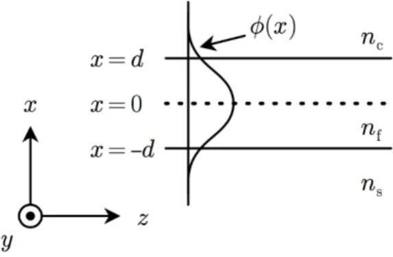
Consider the case where the electromagnetic field component ϕ (x, z) of the light wave propagating in the slab waveguide is separated as follows.
𝜙𝜙(𝜕𝜕, 𝜕𝜕) = 𝜙𝜙(𝜕𝜕)𝑒𝑒
𝑗𝑗𝛽𝛽𝛽𝛽(2.39) Here, 𝛽𝛽 is called a propagation constant and represents the wave number of the light wave propagating in the waveguide. Also, where 𝛽𝛽 = 𝑘𝑘 0 𝑁𝑁 is called the equivalent refractive index or effective refractive index. The equivalent refractive index satisfies the following condition.
𝑚𝑚𝑚𝑚𝜕𝜕 {𝑠𝑠
𝐶𝐶, 𝑠𝑠
𝑆𝑆} < 𝑁𝑁 < 𝑠𝑠
𝑓𝑓(2.40)
Here, an equation representing the dispersion relation of the slab waveguide for each of the TE mode and the TM mode, that is, a dispersion equation is derived.
Figure 3. Beam profile on the three layers of the different material
37 2.8.2.1 TE Mode
Consider the case where the electric field E
y(x, z) is separated as follows.
𝐸𝐸
𝑦𝑦(𝜕𝜕, 𝜕𝜕) = 𝐸𝐸
𝑦𝑦(𝜕𝜕)𝑒𝑒
𝑗𝑗𝛽𝛽𝛽𝛽(2.41)
In the optical waveguide, the light wave is confined in the core and the nearby region, so E
y= 0 at infinity (x = ± ∞). At this time, the general solution of equation (2.35) is expressed by the following equation.
𝐸𝐸
𝑦𝑦= 𝐴𝐴𝑒𝑒
𝑗𝑗��𝑘𝑘0𝑛𝑛2−𝛽𝛽2� 𝛽𝛽+ 𝐵𝐵𝑒𝑒
−𝑗𝑗��𝑘𝑘0𝑛𝑛2−𝛽𝛽2� 𝛽𝛽(2.42)
When the solution that does not diverge at (x = ± ∞) is selected and the electromagnetic field distribution in each region is obtained, it is expressed by the following equation.
𝐸𝐸
𝑦𝑦(𝜕𝜕) = � 𝐸𝐸
𝐶𝐶𝑒𝑒
−𝜎𝜎(𝑥𝑥−𝑑𝑑)(𝜕𝜕 > 𝑑𝑑) 𝐸𝐸
𝑓𝑓𝑐𝑐𝑟𝑟𝑠𝑠(𝜅𝜅𝜕𝜕 − 𝜙𝜙) (−𝑑𝑑 ≤ 𝜕𝜕 ≤ 𝑑𝑑)
𝐸𝐸
𝑆𝑆𝑒𝑒
𝜉𝜉(𝑥𝑥+𝑑𝑑)(𝜕𝜕 < −𝑑𝑑)
(2.43)
Here, σ, κ, ξ are represented by the following equations.
38
⎩ ⎪
⎪ ⎨
⎪ ⎪
⎧𝜎𝜎 = �𝛽𝛽
2− 𝑘𝑘
02𝑠𝑠
𝐶𝐶2= 𝑘𝑘
0�𝑁𝑁
2− 𝑠𝑠
𝐶𝐶2𝜅𝜅 = �𝑘𝑘
02𝑠𝑠
𝑓𝑓2− 𝛽𝛽
2= 𝑘𝑘
0�𝑠𝑠
𝑓𝑓2− 𝑁𝑁
2𝜉𝜉 = �𝛽𝛽
2− 𝑘𝑘
02𝑠𝑠
𝑆𝑆2= 𝑘𝑘
0�𝑁𝑁
2− 𝑠𝑠
𝑆𝑆2(2.44)
Here, since the electromagnetic field is continuous at the boundary of the medium different from the boundary condition expression (2.29), the following boundary condition is satisfied.
𝐸𝐸
𝐶𝐶= 𝐸𝐸
𝑓𝑓𝑐𝑐𝑟𝑟𝑠𝑠(𝜅𝜅𝜕𝜕 − 𝜙𝜙) (2.45) 𝐸𝐸
𝑆𝑆= 𝐸𝐸
𝑓𝑓𝑐𝑐𝑟𝑟𝑠𝑠(𝜅𝜅𝜕𝜕 + 𝜙𝜙) (2.46)
𝜎𝜎𝐸𝐸
𝐶𝐶= 𝜅𝜅𝐸𝐸
𝑓𝑓𝑐𝑐𝑟𝑟𝑠𝑠(𝜅𝜅𝜕𝜕 − 𝜙𝜙) (2.47) 𝜉𝜉𝐸𝐸
𝑆𝑆= 𝜅𝜅𝐸𝐸
𝑓𝑓𝑐𝑐𝑟𝑟𝑠𝑠(𝜅𝜅𝜕𝜕 + 𝜙𝜙) (2.48)
From equations (2.42), (2.44) to (2.47), the following equation is obtained.
𝐸𝐸
𝑦𝑦(𝜕𝜕) = �
𝐸𝐸
𝑓𝑓𝑐𝑐𝑟𝑟𝑠𝑠(𝜅𝜅𝜕𝜕 − 𝜙𝜙) 𝑒𝑒
−𝜎𝜎(𝑥𝑥−𝑑𝑑)(𝜕𝜕 > 𝑑𝑑) 𝐸𝐸
𝑓𝑓𝑐𝑐𝑟𝑟𝑠𝑠(𝜅𝜅𝜕𝜕 − 𝜙𝜙) (−𝑑𝑑 ≤ 𝜕𝜕 ≤ 𝑑𝑑) 𝐸𝐸
𝑓𝑓𝑐𝑐𝑟𝑟𝑠𝑠(𝜅𝜅𝜕𝜕 + 𝜙𝜙) 𝑒𝑒
𝜉𝜉(𝑥𝑥+𝑑𝑑)(𝜕𝜕 < −𝑑𝑑)
(2.49)
39 𝑟𝑟𝑚𝑚𝑠𝑠(𝜅𝜅𝜕𝜕 − 𝜙𝜙) = 𝜎𝜎
𝜅𝜅 (2.50) 𝑟𝑟𝑚𝑚𝑠𝑠(𝜅𝜅𝜕𝜕 − 𝜙𝜙) = 𝜉𝜉
𝜅𝜅 (2.51)
Further, the following equations are obtained from the equations (2.49) and (2.50).
𝜅𝜅𝑑𝑑 = 𝑚𝑚𝑚𝑚 2 +
1
2 𝑟𝑟𝑚𝑚𝑠𝑠
−1� 𝜉𝜉 𝜅𝜅� + 1
2 𝑟𝑟𝑚𝑚𝑠𝑠
−1� 𝜎𝜎
𝜅𝜅� (2.52) 𝜙𝜙 = 𝑚𝑚𝑚𝑚
2 + 1
2 𝑟𝑟𝑚𝑚𝑠𝑠
−1� 𝜉𝜉 𝜅𝜅� −
1
2 𝑟𝑟𝑚𝑚𝑠𝑠
−1� 𝜎𝜎
𝜅𝜅� (2.53) (𝑚𝑚 = 0, 1, 2, 3, ⋯ )
Here, ゙ and m are parameters called mode numbers, and the guided mode corresponding to a certain m is called the m-th mode. Equation (2.41) is the dispersion equation in the TE mode. The propagation constant β can be determined by giving the structure (n
c, n
f, n
s, d), wavelength λ , and mode number m of the optical waveguide.
Next, standardize the dispersion equation and modify it so that it can be applied to any slab waveguide. The normalized frequency V, normalized propagation constant b, and waveguide asymmetry measure a are defined as follows.
𝑉𝑉 = 𝑘𝑘
0𝑑𝑑�𝑠𝑠
𝑓𝑓2− 𝑠𝑠
𝑆𝑆2= 𝑗𝑗𝑑𝑑
𝑐𝑐 �𝑠𝑠
𝑓𝑓2− 𝑠𝑠
𝑆𝑆2(2.54)
40 𝑏𝑏 = 𝑁𝑁
2− 𝑠𝑠
𝑆𝑆2𝑠𝑠
𝑓𝑓2− 𝑠𝑠
𝑆𝑆2(2.55) 𝑚𝑚 = 𝑠𝑠
𝑆𝑆2− 𝑠𝑠
𝐶𝐶2𝑠𝑠
𝑓𝑓2− 𝑠𝑠
𝑆𝑆2(2.56)
By transforming equation (2.51) using equations (2.53) to (2.55), the following standardized dispersion equation is obtained.
2𝑉𝑉√1 − 𝑏𝑏 = 𝑚𝑚𝑚𝑚 + 𝑟𝑟𝑚𝑚𝑠𝑠
−1� 𝑏𝑏
1 − 𝑏𝑏 + 𝑟𝑟𝑚𝑚𝑠𝑠
−1�𝑚𝑚 + 𝑏𝑏
1 − 𝑏𝑏 (2.57)
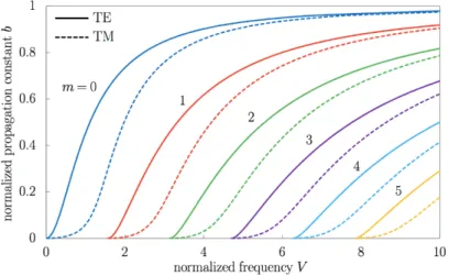
Fig. 4 shows the b-V curve obtained from equation (2.56). From Figure 4 the
zero-order mode exists for every V when a = 0, that is, when n
S= n
C. That is, at
least one waveguide mode exists in a slab waveguide having a symmetric refractive
index distribution. On the other hand, the other modes do not exist in the region
below a certain V. Such a state is called a cutoff.
41 Figure 4. Normalized propagation constant dependence of the normalize
frequency on TE and TM mode.
2.8.2.2 TM Mode
As in the case of the TE mode, the solution of equation (2.38) yields the following equation.
𝐻𝐻
𝑦𝑦(𝜕𝜕) = � 𝐻𝐻
𝐶𝐶𝑒𝑒
−𝜎𝜎(𝑥𝑥−𝑑𝑑)(𝜕𝜕 > 𝑑𝑑) 𝐻𝐻
𝑓𝑓𝑐𝑐𝑟𝑟𝑠𝑠(𝜅𝜅𝜕𝜕 − 𝜙𝜙) (−𝑑𝑑 ≤ 𝜕𝜕 ≤ 𝑑𝑑)
𝐻𝐻𝑒𝑒
𝜉𝜉(𝑥𝑥+𝑑𝑑)(𝜕𝜕 < −𝑑𝑑)
(2.58)
Here, σ, κ, ξ are represented by the following equations.
42
⎩ ⎪
⎪ ⎨
⎪ ⎪
⎧𝜎𝜎 = �𝛽𝛽
2− 𝑘𝑘
02𝑠𝑠
𝐶𝐶2= 𝑘𝑘
0�𝑁𝑁
2− 𝑠𝑠
𝐶𝐶2𝜅𝜅 = �𝑘𝑘
02𝑠𝑠
𝑓𝑓2− 𝛽𝛽
2= 𝑘𝑘
0�𝑠𝑠
𝑓𝑓2− 𝑁𝑁
2𝜉𝜉 = �𝛽𝛽
2− 𝑘𝑘
02𝑠𝑠
𝑆𝑆2= 𝑘𝑘
0�𝑁𝑁
2− 𝑠𝑠
𝑆𝑆2(2.59)
Although the electromagnetic field is continuous at the boundary between different media, since
1n2
𝜕𝜕𝐻𝐻𝐻𝐻
𝜕𝜕𝑥𝑥
is continuous instead of H
yfrom equation (2.37), the following equation is obtained.
𝐻𝐻
𝐶𝐶= 𝐻𝐻
𝑓𝑓𝑐𝑐𝑟𝑟𝑠𝑠(𝜅𝜅𝜕𝜕 − 𝜙𝜙) (2.60)
𝐻𝐻
𝑆𝑆= 𝐻𝐻
𝑓𝑓𝑐𝑐𝑟𝑟𝑠𝑠(𝜅𝜅𝜕𝜕 + 𝜙𝜙) (2.61)
𝜎𝜎𝑠𝑠
𝐶𝐶2𝐸𝐸
𝐶𝐶= 𝜅𝜅𝑠𝑠
𝑓𝑓2𝐻𝐻
𝑓𝑓𝑐𝑐𝑟𝑟𝑠𝑠(𝜅𝜅𝜕𝜕 − 𝜙𝜙) (2.62)
𝜉𝜉𝑠𝑠
𝑆𝑆2𝐸𝐸
𝑆𝑆= 𝜅𝜅𝑠𝑠
𝑓𝑓2𝐻𝐻
𝑓𝑓𝑐𝑐𝑟𝑟𝑠𝑠(𝜅𝜅𝜕𝜕 + 𝜙𝜙) (2.63)
The following equations are obtained from Equations (2.57) to (2.62).
𝐻𝐻
𝑦𝑦(𝜕𝜕) = �
𝐻𝐻
𝑓𝑓𝑐𝑐𝑟𝑟𝑠𝑠(𝜅𝜅𝜕𝜕 − 𝜙𝜙) 𝑒𝑒
−𝜎𝜎(𝑥𝑥−𝑑𝑑)(𝜕𝜕 > 𝑑𝑑) 𝐻𝐻
𝑓𝑓𝑐𝑐𝑟𝑟𝑠𝑠(𝜅𝜅𝜕𝜕 − 𝜙𝜙) (−𝑑𝑑 ≤ 𝜕𝜕 ≤ 𝑑𝑑) 𝐻𝐻
𝑓𝑓𝑐𝑐𝑟𝑟𝑠𝑠(𝜅𝜅𝜕𝜕 + 𝜙𝜙) 𝑒𝑒
𝜉𝜉(𝑥𝑥+𝑑𝑑)(𝜕𝜕 < −𝑑𝑑)
(2.64)
43 𝑟𝑟𝑚𝑚𝑠𝑠(𝜅𝜅𝜕𝜕 − 𝜙𝜙) = 𝜎𝜎𝑠𝑠
𝑓𝑓2𝜅𝜅𝑠𝑠
𝐶𝐶2(2.65) 𝑟𝑟𝑚𝑚𝑠𝑠(𝜅𝜅𝜕𝜕 − 𝜙𝜙) = 𝜉𝜉𝑠𝑠
𝑓𝑓2𝜅𝜅𝑠𝑠
𝑆𝑆2(2.66)
From equations (2.64) and (2.65), a dispersion equation for the TM mode is obtained by the following equation.
𝜅𝜅𝑑𝑑 = 𝑚𝑚𝑚𝑚 2 +
1
2 tan
−1� 𝜉𝜉𝑠𝑠
𝑓𝑓2𝜅𝜅𝑠𝑠
𝑆𝑆2� + 1
2 tan
−1� 𝜎𝜎𝑠𝑠
𝑓𝑓2𝜅𝜅𝑠𝑠
𝐶𝐶2� (2.67)
𝜅𝜅𝑑𝑑 = 𝑚𝑚𝑚𝑚 2 +
1
2 tan
−1� 𝜉𝜉𝑠𝑠
𝑓𝑓2𝜅𝜅𝑠𝑠
𝑆𝑆2� − 1
2 tan
−1� 𝜎𝜎𝑠𝑠
𝑓𝑓2𝜅𝜅𝑠𝑠
𝐶𝐶2� (2.68) (𝑚𝑚 = 0, 1, 2, 3, ⋯ )
Also, as in the case of the TE mode, Expression (3.63) is normalized using Expressions (2.53) to (2.55). The normalized TM mode dispersion equation is shown below.
2𝑉𝑉 = √1 − 𝑏𝑏 = 𝑚𝑚𝑚𝑚 + 𝑟𝑟𝑚𝑚𝑠𝑠
−1� 𝑠𝑠
𝑓𝑓2𝑠𝑠
𝑆𝑆2� 𝑏𝑏
1 − 𝑏𝑏� + 𝑟𝑟𝑚𝑚𝑠𝑠
−1� 𝑠𝑠
𝑓𝑓2𝑠𝑠
𝐶𝐶2�𝑚𝑚 + 𝑏𝑏
1 − 𝑏𝑏� (2.69)
Figure 4 shows dispersion curves of the TE mode and the TM mode when
n
f= 3.47, n
S= n
C= 1.44, and a = 0. While the normalized dispersion curve of the
44 TE mode does not depend on the refractive index of the waveguide material, the rise of the curve becomes gentler as the relative refractive index difference increases in the TM mode.
Figure 4. Normalized propagation constant dependence of the normalize frequency on TE and TM mode.
2.9 Finite Different Time Domain
The Finite Difference Time Domain method (FDTD) is a method of
discretizing the time-domain analysis formula of Maxwell's equation in space and
time, and numerically calculating it as a difference equation. Since no
45 approximation other than discretization is included, the calculation accuracy is good under sufficiently fine difference width. In addition, since it is a numerical analysis method in the time domain, it is possible to perform a spectrum analysis by one simulation by performing a Fourier transform on the obtained solution.
Although it is a method that is easy to implement but requires a large amount of computation, it is now considered to be the mainstream numerical calculation algorithm for electromagnetic field analysis due to recent improvements in computer performance.
In this research, the FDTD method is uses in simulation software to do some calculation, and the software has included all the theoretical calculations. So that, the simulation software helps to develop and analysis deeply in the characteristics of the slab waveguide.
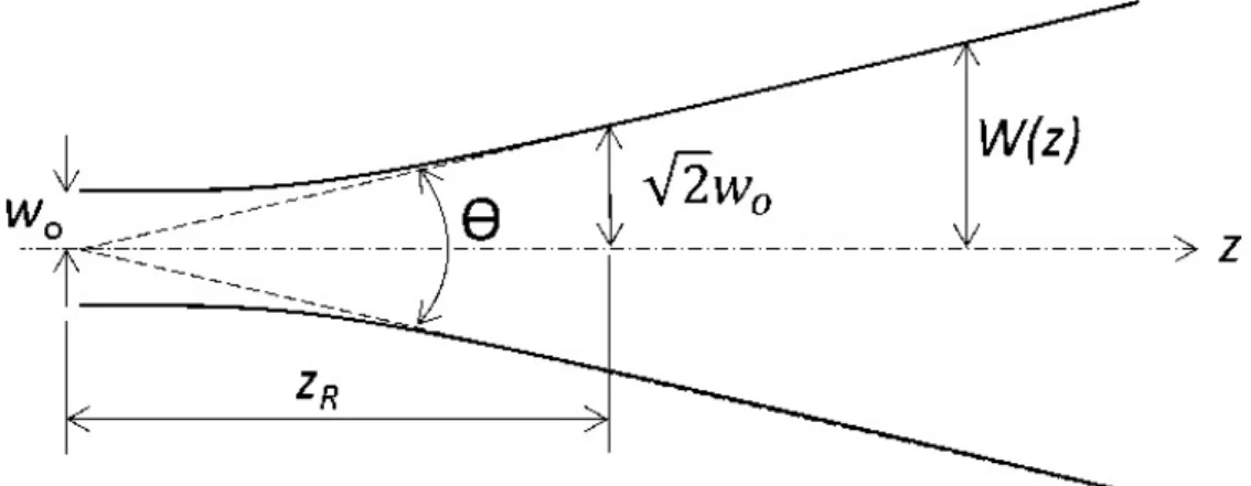
2.10 Gaussian Beam and Beam Divergence
In most applications, the propagation characteristics of laser beam is necessary to be known. In general, laser beam propagation can be assuming that the laser beam has an ideal Gaussian intensity profile that can be expressed as
𝐼𝐼(𝑟𝑟) = 𝐼𝐼(0)𝑒𝑒𝜕𝜕𝑒𝑒 �−
𝜔𝜔2𝑟𝑟202
�, (2.70)
46 where r is defined as the distance from the center of the beam, and 𝑗𝑗
0is the radius at which the amplitude is
1e
of its value on the axis.
Figure 5. Gaussian beam propagation in free space
From the Fig. 5, a Gaussian beam propagating in free space, the spot size w(z) will be at minimum value w
oat a place along the beam axis, known as the beam waist . For a beam of wavelength λ at a distance z along the beam from the beam waist, it is also called the edge of a beam radius where r = w(z), the variation of the spot size is given by:
𝑤𝑤(𝜕𝜕) = 𝑤𝑤
𝑜𝑜�1 + �
𝛽𝛽𝛽𝛽𝑅𝑅
�
2, (2.71)
47 where the origin of the z-axis is defined without loss of generally to coincide with the beam waist, and the Rayleigh distance or Rayleigh range 𝜕𝜕
𝑅𝑅is determined by 𝜕𝜕
𝑅𝑅=
𝜋𝜋𝑤𝑤𝜆𝜆𝑜𝑜2. (2.72)
Therefore, the condition where 𝜕𝜕 ≫ 𝜕𝜕
𝑅𝑅the parameter w(z) increases linearly with z. It is mean that far from waist, the beam edge is cone-shaped. The angle between lines along that cone and the central axis of the beam is called divergence of the beam, that given by
𝜃𝜃 ≈
𝜋𝜋𝜔𝜔𝜆𝜆00𝑛𝑛
, (2.73) where, n is the refractive index of the medium the beam propagates through, and 𝜆𝜆
0is the free-space wavelength. When the directivity angle is sufficiently small, the total angular spread of the beam far from the waist, and is given by
𝛩𝛩 = 2𝜃𝜃 = 2𝑟𝑟𝑚𝑚𝑠𝑠
−1� 𝜆𝜆
0𝑚𝑚𝑗𝑗
0𝑠𝑠� ≈ 2𝑟𝑟𝑚𝑚𝑠𝑠
−1� 𝐷𝐷
𝑓𝑓− 𝐷𝐷
𝑖𝑖2𝐿𝐿 � . (2.74)
The divergence of a beam also can be calculated if one knows the beam diameter
at two separate points far from any focus D
iand D
fon distance L between these
points.
48
2.10.1 Collimated Beam
A collimated beam of light is a beam typically a laser beam, which has a low beam divergence so that the beam radius does not undergo significant changes within reasonable propagation distance. In the case of Gaussian beams, the Rayleigh length must be long compared with the envisaged propagation distance.
The Rayleigh length scales with the square of the beam waist radius so that large beam radius is essential for long propagation distances.
A divergent beam can merely be collimated with a lens or a curved mirror, where the focal length or curvature radius is chosen such that the curved initially wave fronts become flat, which can be seen in Figure 6.
Figure 6. A doubled lens collimates the output beam from a fiber
49 Collimated beams are very useful to emitting in long distance for several applications like wireless power or data transfer, because the beam radius stays approximately constant, so that the distances between optical components may be readily varied without applying extra optics, and excessive beam radius is avoided.
Most solid-state lasers naturally emit collimated beams, a flat output coupler enforces flat wave fronts at the output, and the beam waist is usually large enough to avoid excessive divergence. Edge-emitting laser diodes, however, emit strongly diverging beams and are therefore often equipped with collimation optics, with a collimator, largely reducing the strong divergence.
The analysis about the collimated beam is very useful in discussing about the
taper design in slab waveguide. The details of the taper design will be explained in
the chapter. 3
50
Chapter 3
Design and Simulation
3.1 Introduction
The slab waveguide consists of three layers of materials with different dielectric constants, extending infinitely in the directions parallel to their interfaces.
The light may be confined in the middle layer by total internal reflection. This occurs only if the dielectric index of the middle layer is larger than that of the surrounding layers. In practice slab waveguides are not infinite in the direction parallel to the interface, but if the typical size of the interfaces is much larger than the depth of the layer, the slab waveguide model will be an excellent approximation.
On the application, the function and characteristics of a slab waveguide are
determined by its design. The constructed design by using taper to connect channel
waveguide to slab waveguide as shown in Fig. 7
51 Figure 7. Cross section of a slab waveguide
In its application it is very difficult to guide the light that comes directly inside the slab waveguide, considering the confinement factor in the slab waveguide is only limited to 1-dimension. For this reason, many researchers propose using a grating coupler or spot size converter, meanwhile from the design side to be propagated use taper design.
Figure 8. Cross section of a slab waveguide
SiO2
Si 0.21
µm
Air
x y
z
x
0.4 µm
SiO
2Si y
125 µm
L
L
10 µm
z
52 The slab waveguide which is connected with the channel waveguide, with 0.4 µm in width and 0.21 µm in thickness as shown in Fig. 8. The slab waveguide is constructed by the Si as a core and SiO
2as the substrate. The taper design with 125 µm in length, 0.4 µm of input port, and 10 µm of output port is designed after the channel to keep the light propagates in parallel. The slab waveguide is constructed of silicon with an effective refractive index (n
eff) of 2.83 as a core and SiO
2with a refractive index of (n) 1.47 as the substrate. The refractive index difference makes the light to propagate to the x-direction inside of the silicon waveguide only.
3.2 Design
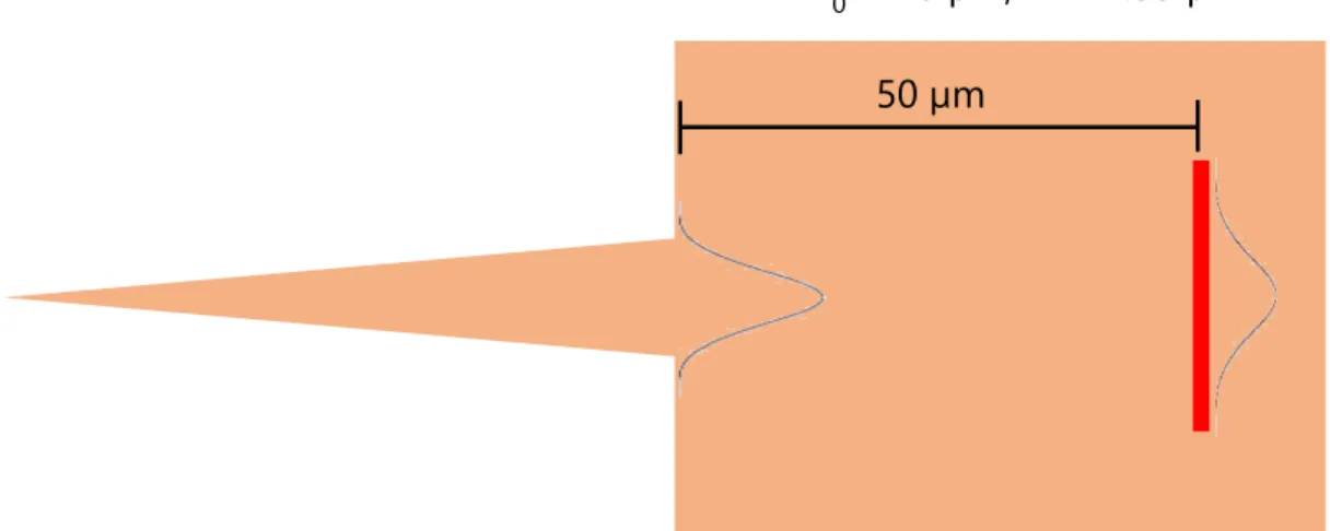
3.2.1. Taper design
The function of the taper is to obtain an efficient coupling between two different optical waveguides which are channel waveguide and the slab waveguide.
Normally, the function of the taper is to change the size and the shape of the optical propagation. The linear taper is adapted to this design as shown in Fig. 9.
53 Figure 9. The taper design on the slab waveguide
The taper design with 125 µm in length, 0.4 µm of the input port, and 10 µm of the output port is designed after the channel waveguide to control the divergence angle of the input light of slab waveguide. Using taper structure, the divergence angle of the input light of slab waveguide can be kept small.
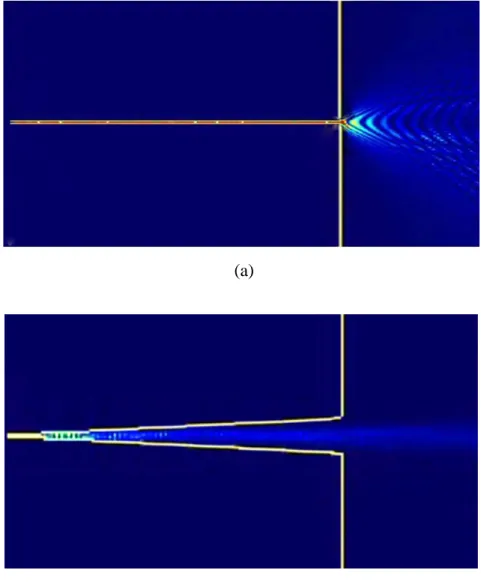
The tapered design carries out the parallel pattern of the light with small divergence angle, even though the output beam size is larger than the input as shown in Fig. 10.
y
z x
Channel waveguide Linear taper Slab waveguide SiO Si
2