INVITED PAPER
Joint Special Section on Opto-electronics and Communications for Future Optical NetworkWavelength-Routed Switching for 25-Gbit / s Optical Packets Using a Compact Transmitter Integrating a Parallel-Ring-Resonator
Tunable Laser and an InGaAlAs EAM
Toru SEGAWA†a), Wataru KOBAYASHI†,Members, Tatsushi NAKAHARA†,Nonmember, andRyo TAKAHASHI†,Member
SUMMARY We describe wavelength-routed switching technology for 25-Gbit/s optical packets using a tunable transmitter that monolithically in- tegrates a parallel-ring-resonator tunable laser and an InGaAlAs electro- absorption modulator (EAM). The transmitter provided accurate wave- length tunability with 100-GHz spacing and small output power variation.
A 25-Gbit/s burst-mode optical-packet data was encoded onto the laser output by modulating the integrated EAM with a constant voltage swing of 2 V at 45◦C. Clear eye openings were observed at the output of the 100 GHz-spaced arrayed-waveguide grating with error-free operation be- ing achieved for all packets. The tunable transmitter is very promising for realizing a high-speed, large-port-count and energy-efficient wavelength- routing switch that enables the forwarding of 100-Gbit/s optical packets.
key words: tunable laser, electro-absorption modulator, optical packet switching, photonic integrated circuits
1. Introduction
The rapid increase of data traffic in optical communica- tions networks due to the widespread use of the Internet and Internet-related services has led to a need for large- capacity and low-power-consumption nodes with various traffic-engineering capabilities. In particular, current intra- data center networks based on electrical switches/routers face a continuous increase in network traffic due to the rise of cloud computing and other emerging web applications, and require excessive power levels to sustain the traffic in- crease [1]. Optical packet-switched networks (OPS-NWs) that rely on optical packet routers are considered a potential solution that can maximize the flexibility and throughput of the network owing to the packet-level granularity [2]–[4].
However, the implementation of OPS-NWs requires opti- cal routers that surpass the performance of current electrical routers.
We have previously constructed an 8×8 hybrid op- toelectronic router (HOPR) prototype that combines the strength of optical and electrical technologies [5]. We demonstrated error-free routing of 10-Gbit/s asynchronous arbitrary-length optical packets together with high-level functions such as Quality of Service (QoS) provisioning and packet multicasting, while achieving low power con-
Manuscript received November 14, 2013.
Manuscript revised January 31, 2014.
†The authors are with NTT Photonics Laboratories, Atsugi-shi, 243-0198 Japan.
a) E-mail: [email protected] DOI: 10.1587/transele.E97.C.719
sumption and low latency. One of the key devices in HOPR is a high-speed N×N optical switch operating on a packet-by-packet basis for forwarding incoming optical packets to desired output ports [6]. An N × N optical switch in an optical router should ideally have small size, low power consumption, high-speed switching capability, data-format transparency, high reliability and scalability, as well as ease of control and low cost. Aiming at realiz- ing such an ideal optical switch, so far, a variety of optical switching technologies have been proposed, including opti- cal switches consisting of cascading 1×2/2×2 switches in crossbar/tree/Benes/Banyan architecture [7], broadcast-and- select switches [8], wavelength-routing switches [9] and phased-array switches [10]. Among these optical switching technologies, the wavelength-routing switch is attractive as its port count can be increased without additional loss, and would thus allow a higher throughput.
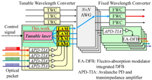
Figure 1 shows the architecture of the N × N wavelength-routing switch being developed for 100-Gbit/s (25-Gbit/s×4λ) optical packets. The switch consists of tunable wavelength converters (TWC), a cyclic arrayed- waveguide grating (AWG), and fixed wavelength converters (FWC). Within the switch, the label-swapped packet first enters TWC consisting of a tunable laser and an array of four burst-mode receiver front-ends (APD-TIAs), together with driver amplifiers, and electro-absorption modulators (EAMs). The tunable laser output is divided into four parts, modulated by the EAMs, and connected to four planes of wavelength-cyclic AWGs. Control signals from the sched- uler tune the wavelength of the laser to enable the desired path across the AWGs. Having the AWGs equipped with a
Fig. 1 N×Noptical switch architecture for 100-Gbit/s (25-Gbit/s×4λ).
Copyright c⃝2014 The Institute of Electronics, Information and Communication Engineers
tunable laser at each input port enables non-blockingN×N wavelength-based switching. The packet data encoded onto the tunable laser output is routed to the desired AWG out- put port, and then received by the FWC that consists of an APD-TIA equipped with a driver amplifier, and an EA-DFB laser; to convert the signal wavelength back to the original input wavelength.
Within the TWC, the wavelengths of optical pack- ets are changed on a packet-by-packet basis, thus the lasing wavelength of the tunable laser should be tuned within several nanoseconds. So far, several types of tunable lasers have been demonstrated, including the sampled-grating/super-structure-grating distributed-Bragg- reflector (SG/SSG DBR) lasers [11], [12], digital supermode (DS) DBR lasers [13], modulated grating Y-branch (MGY) lasers [14], and grating coupler with rear sampled grating reflector (GCSR) lasers [15]. These lasers have a common tuning mechanism based on the free-carrier plasma effect produced by current injection, which changes the refrac- tive indices of the tuning sections. However, the lasing- wavelength drift caused by the transient thermal effect re- mains a problem [16]. The wavelength drift has a much longer response time (millisecond order) compared to the mechanism employed for fast tuning.
In our previous work, a double-ring-resonator tunable laser (DRR-TL) was developed for use as a high-speed tun- able light source [17]. Compared to the DBR-type filters, the ring-resonator filters employed in the cavity of the DRR- TL exhibit superior filtering characteristics in addition to the advantage of having a compact structure [18], [19]. These characteristics include a narrower transmission bandwidth with a Lorentzian-type filter response and an infinite num- ber of resonant peaks in the transmission spectrum. The rapid (less than 11 ns) and stable wavelength tuning (wave- length drift of less than 5 GHz) achieved by the low tun- ing current of the DRR-TL enables the realization of a fast, scalable, and low-powerN×Noptical switch [17], [20]. A shortcoming of the DRR-TL is that the output power varies during tuning due to the free-carrier absorption.
To solve this issue, we have recently developed a parallel-ring-resonator tunable laser (PRR-TL) [21]. The PRR-TL provided small output power variation of less than 1 dB over a wide tuning range of 35 nm. As a proof of con- cept, a transmitter that monolithically integrates the PRR- TL with an InGaAlAs EAM was developed. Error-free op- eration at 25 Gbit/s with a dynamic extinction ratio of more than 10 dB was achieved with a constant voltage swing of 2 V over a tuning range of 25.7 nm under the semi-cooled condition (45◦C) [21].
In this paper, we review the tunable transmitter that enables high-speed wavelength switching operation. We demonstrate error-free 1×4 optical packet switching, for 25- Gbit/s burst-mode optical packets of different lengths (20–
100 ns), by using a 100 GHz-spaced AWG and the transmit- ter. This paper is organized as follows. Section 2 describes the operation principle and the fabrication of the transmit- ter in which the PRR-TL and EAM are monolithically in-
Device size: 1.4 x 0.35 mm2
EAM Filter section
Gain section Phase
PRR-TL
Ring1 Ring2
Etched front mirror
Fig. 2 Photograph of the fabricated tunable transmitter.
tegrated. Section 3 describes the high-speed wavelength- routed switching operation for the 25-Gbit/s optical packets.
Section 4 summarizes the main points.
2. Tunable Transmitter
Figure 2 shows a photograph of the fabricated tunable trans- mitter consisting of the PRR-TL and an EAM. The PRR- TL includes a gain section, a phase-control section and two ring resonators placed in parallel with slightly different free spectral ranges (FSRs) designed as 200 and 222 GHz, re- spectively. The laser cavity of the PRR-TL is defined by an etched mirror [22] used as the front mirror and a reflective filter section. More about the structure and design of the etched mirror can be found in Ref. [20]. In the filter section, each ring resonator plays the role of a wavelength selective filter as well as a loop-mirror in a Mickelson interferometer that is a part of the laser cavity.
In our previous work [17], two ring resonators were cascaded as shown in Fig. 3(a). In that DRR filter, the wave- length tuning range∆λis expanded by the Vernier effect.∆λ is expressed as
∆λ=M·FSR1=N·FSR2, (1)
M= FSR2
FSR2−FSR1, (2)
N= FSR1
FSR2−FSR1, (3)
where FSR1 and FSR2 are the FSR of Ring1 and Ring2, respectively. M andN are the number of resonance peak spacings within∆λof Ring1 and Ring2, respectively, and are written as,
M−N=1. (4)
On the other hand, in the PRR configuration (Fig. 3(b)), the filter produces constructive (in-phase) and destructive (out-of-phase) interferometric characteristics in the reflec- tion spectrum. Figure 4(a) shows the calculated reflection spectrum from the PRR filter section. In this calculation, FSR1 and FSR2 are set as 200 GHz and 222 GHz, respec- tively. The interferometric characteristics can be seen re- peated every 2∆λ. Figure 4(b) shows a schematic diagram of a single ring resonator and Fig. 4(c) shows the calculated transmittance and relative phase for the drop port of the ring
2x2 coupler )
b ( )
a (
Back mirror Ring1
Gain section
Ring1
Ring2 Gain section Ring2
Fig. 3 Two filter configuration. (a) Double-ring resonator (DRR). (b) Parallel-ring resonator (PRR).
-50 -40 -30 -20 -10 0 10
1.53 1.535 1.54 1.545 1.55 1.555 1.56
Reflectivity (dB)
Wavelength (µm)
Maximum reflectivity (in-phase)
Minimum reflectivity (out-of-phase)
∆λ
∆R
(a)
-12 -10 -8 -6 -4 -2 0
-1 -0.5 0 0.5 1
1.548 1.549 1.55 1.551 1.552
Transmittance (dB) Relative phase (㽢π)
Wavelength (µm) π
(b) (c)
Input port
Drop port
Through port (not used)
Fig. 4 (a) Calculated reflection spectrum from the PRR filter section, (b) schematic diagram of a single ring resonator, and (c) transmission spectrum and relative phase for the drop port of the ring resonator.
resonator. The ring resonator raises a phase difference ofπ between its peak wavelengths. Even if the ring resonator is a part of the loop mirror by connecting the input and drop port to the 2×2 coupler as shown in Fig. 3(b), the transmis- sion and phase characteristics of the ring resonator are main- tained. Thus, the tuning range is double that of the DRR filter with the same FSRs due to the difference between M andNas given in Eq. (4).
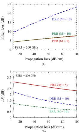
In the PRR filter, the light passes through the ring res- onator only once compared to four times in the DRR filter.
Therefore, the PRR filter is expected to have a larger reflec- tivity than the DRR filter. Figure 5(a) shows the calculated filter loss for the PRR and DRR filters as a function of the propagation loss of the waveguide composing their ring res- onators. In this calculation, FSR1 is set to be 200 GHz with anMof 10 for the DRR filter, and an Mof 5 or 10 for the PRR filter. The filter loss increases with propagation loss for both the DRR and PRR filters, however the filter loss is clearly lower for the PRR filter. One possible disadvantage of using the PRR configuration may be the low wavelength selectivity due to the small count of light pass through the ring resonator. The peak-reflectivity difference∆Rbetween the resonant peak and its adjacent peak (Fig. 4) must be high
0 5 10 15 20 25
20 40 60 80 100
Filter loss (dB)
Propagation loss (dB/cm) PRR (M = 5) PRR (M = 10)
FSR1 = 200 GHz
DRR (M = 10)
(a)
0 0.5 1 1.5 2 2.5 3 3.5 4
20 40 60 80 100
∆R(dB)
Propagation loss (dB/cm)
FSR1 = 200 GHz
PRR (M = 5)
PRR (M = 10) DRR (M = 10)
(b)
Fig. 5 Calculated (a) the filter loss and (b)∆Rof the PRR and DRR filter as a function of the propagation loss of the waveguide section.
enough for stable lasing, because a low∆Rwould result in a small side-mode suppression ratio (SMSR) of the tunable laser. Figure 5(b) shows the calculated∆Rvalue for the PRR and DRR filters as a function of the propagation loss of their waveguides. FSR1 and M are the same in the calculation shown in Fig. 4(a). Compared to the DRR filter, the PRR filter with the same M has a small∆R. However as could be seen from Eq. (1), the PRR filter which provides twice the tuning range of the DRR filter, can be set to have half the value of M of the DRR filter while keeping the same
∆λ. In this case, the PRR filter provides a lager∆Rthan the DRR filter as shown in Fig. 5(b); hence improving the filter performance.
For the PRR-TL section, a stack-layer structure is used [17], in which a layer of InGaAsP multiple-quantum- wells (MQWs) with upper and lower separate-confinement hetero-structure (SCH) layers are grown on top of a 0.3 µm-thick InGaAsP layer (λg =1.4µm) for the active sec- tion. The length of the gain section is 400µm. The gain and phase sections have a shallow-ridge waveguide struc- ture whereas the ring resonators have a deep-ridge one [17].
On the other hand, InGaAlAs MQWs are used in the EAM section to achieve 25-Gbit/s operation with a sufficient ex- tinction ratio over a wide wavelength range. These MQWs have a large conduction band offset and a small valence band offset compared with InGaAsP MQWs; resulting in a steep extinction curve and large E/O frequency bandwidth [23].
The EAM section composed of InGaAlAs MQWs is directly
Fig. 6 Superimposed lasing spectra of the fabricated tunable transmitter.
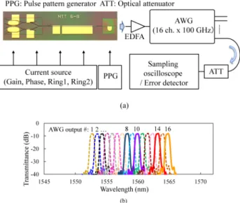
Fig. 7 (a) Experimental setup for demonstrating 1×Noptical packet switching. (b) Transmission spectra of the AWG.
butt-jointed to the PRR-TL section. This enables fabrication with only one additional re-growth step after the formation of the PRR-TL section, and allows the independent design of the PRR-TL and EAM. The PRR-TL and EAM sections were designed with epitaxial structures optimized to have the transmitter operating in the C-band. The EAM section has the same shallow-ridge waveguide structure as the gain and phase sections. The length of the EAM section is 150 µm. The EAM section is buried with BCB to reduce the capacitance of the EAM section, and thereby the frequency bandwidth is extended up to 39 GHz [23]. The electrodes are then formed by a liftoffprocess.
3. Switching Demonstration
Figure 6 shows the superimposed lasing spectra of the trans- mitter operating in a CW mode at 45◦C. The current injected to the gain section was kept constant at 100 mA. The lasing output was coupled into a lensed fiber and detected with an optical spectrum analyzer. By tuning the current of Ring1, Ring2, and phase control section, 24-channel lasing oper- ation with 100-GHz channel spacing was achieved with a
Fig. 8 Packet stream waveforms of (a) the transmitter output and (b)–(e) the AWG outputs.
side-mode suppression ratio larger than 40 dB. The result indicates that the laser is promising for a large-port-count wavelength-routing switch.
Figure 7(a) illustrates the experimental setup for demonstrating 1×N optical packet switching. Dynamic wavelength switching was performed by modulating the current injected only to Ring2 with a multi-level voltage signal generated by an arbitrary waveform generator. A 25- Gbit/s burst-mode optical packet stream containing four re- peated packets (packet 1–4) with various lengths (20–100 ns) and an inter-packet guard band of 20 ns was generated by modulating the EAM with a DC bias level of −1.7 V and voltage swing of 2.0 V. The packets have non-return- to-zero (NRZ) format with a 27 −1 PRBS pattern. The optical packet stream was fed into a 16-channel 100 GHz- spaced AWG to perform 1×Noptical packet switching. In this experiment, four channels (output 8, 10, 14, and 16) of the AWG were employed (Fig. 7(b)). Figure 8(a) shows the packet waveforms at the transmitter output, indicating small output power variation among packets due to the small free-carrier-absorption loss in the ring resonators that is still limited even at high-speed switching. Figure 8(b)–(e) show the waveforms of the packets output from different AWG ports, whereas Fig. 9(a) shows the eye diagram of each out- put packet in which clear eye openings were observed. As shown in Fig. 9(b) error measurement was done for each packet individually; confirming the error-free operation at
Fig. 9 (a) Eye diagrams for the four output port of the AWG. (b) BER results.
25-Gbit/s optical packet switching.
4. Summary
We have described a 25-Gbit/s, 1×4 wavelength-routed optical packet switching based on a tunable transmitter that monolithically integrates a PRR-TL with an InGaAlAs EAM. The PRR-TL provided accurate wavelength tunabil- ity with 100-GHz spacing and small output power varia- tion. PRBS data was encoded onto the TL output by mod- ulating the integrated EAM with a constant voltage swing of 2 V at 45◦C. Clear eye openings were observed for the four output ports of the AWG, and error-free operation was achieved for the packets at all wavelengths. The results clarify that the tunable transmitter is very promising for re- alizing a high-speed, large-port-count and energy-efficient wavelength-routing switch that enables the forwarding of 100-Gbit/s optical packets.
Acknowledgments
This work was partially supported by the National Institute of Information and Communications Technology (NICT).
References
[1] C. Kachris, K. Kanonakis, and I. Tomkos, “Optical interconnection networks in data centers: recent trends and future challenges,” IEEE Communications Magazine, vol. 51, no. 9, pp. 39–45, Sept. 2013.
[2] S. J. B. Yoo, “Optical packet and burst switching technologies for the future photonic internet,” J. Lightwave Technol., vol. 24, no. 12, pp. 4468–4492, Dec. 2006.
[3] R. Takahashi, T. Nakahara, K. Takahata, H. Takenouchi, T. Yasui, N.
Kondo, and H. Suzuki, “Ultrafast optoelectronic packet processing for asynchronous, optical-packet-switched networks,” OSA J. Opt.
Netw., vol. 3, no. 12, pp. 914–930, Dec. 2004.
[4] Y. Yin, R. Proietti, X. Ye, C. J. Nitta, V. Akella, and S. J. B. Yoo,
“LIONS: An AWGR-based low-latency optical switch for high- performance computing and data centers,” IEEE J. Sel. Topics.
Quantum Electron., vol. 19, no. 2, pp. 3600409, Mar./Apr. 2013.
[5] H. Takenouchi, R. Urata, T. Nakahara, T. Segawa, H. Ishikawa, and R. Takahashi, “First demonstration of a prototype hybrid optoelec- tronic router,” in Proceedings of 35th European Conference on Op- tical Communication (ECOC), PD3.2, 2009.
[6] R. Urata, T. Nakahara, H. Takenouchi, T. Segawa, H. Ishikawa, A.
Ohki, H. Sugiyama, S. Nishihara, and R. Takahashi, “4×4 optical packet switching with a prototype 4×4 label processing and switch- ing sub-system,” in Proceedings of 35th European Conference on Optical Communication (ECOC), 6.3.1, 2009.
[7] G. I. Papadimitriou, C. Papazoglou, and A. S. Pomportsis, “Optcial siwthing,” Wiley-Interscience, 2006.
[8] P. Gambini, M. Renaud, C. Guillemot, F. Callegati, I. Andonovic, B. Bostica, D. Chiaroni, G. Corazza, S. Danielsen, P. Gravey, P.
B. Hansen, M. Henry, C. Janz, A. Kloch, R. Krahenbuhl, C. Raf- faelli, M. Schilling, A, Talneau, and L. Zucchelli, “Transparent opti- cal packet switching: network architecture and demonstrators in the KEOPS project,” IEEE J. Select. Areas Commun., vol. 16, no. 7, pp. 1245–1259, Sept. 1998.
[9] J. Gripp, M. Duelk, J. E. Simsarian, A. Bhardwaj, P. Bernasconi, O.
Laznicka, and M. Zirngibl, “Optical switch fabrics for ultra-high- capacity IP routers,” J. Lightwave Technol. vol. 21, no. 11, pp. 2839–
2850, Nov. 2003.
[10] M-J. Kwack, T. Tanemura, A. Higo, and Y. Nakano, “Monolithic InP strictly non-blocking 8×8 switch for high-speed WDM optical interconnection,” in Proceedings of 38th European Conference on Optical Communication (ECOC), Th.3.B.3, 2012.
[11] V. Jayaraman, Z. M. Chuang, and L. Coldren, “Theory, design, and performance of extended tuning range semiconductor lasers with sampled gratings,” IEEE J. Quantum Electron., vol. 29, no. 6, pp. 1824–1834, June 1993.
[12] H. Ishii, Y. Tohmori, Y. Yoshikuni, T. Tamamura, and Y. Kondo,
“Multiple-phase-shift super structure grating DBR lasers for broad wavelength tuning,” IEEE Photon. Technol. Lett., vol. 5, no. 6, pp. 613–615, June 1993.
[13] D. J. Robbins, G. Busico, E. Barton, L. Ponnampalam, J. P. Duck, N. D. Whitbread, P. J. Williams, D. C. J. Reid, A. C. Carter, and M.
J. Wale, “Widely tunable DS-DBR laser with monolithically inte- grated SOA: Design and performance,” IEEE J. Sel. Top. Quantum Electron., vol. 11, no. 1, pp. 149–156, Jan./Feb. 2005.
[14] R. Laroy, G. Morthier, T. Mullane, M. Todd, and R. Baets, “Stabil- isation and control of widely tunable MG-Y lasers with integrated photodetectors,” IET Optoelectron., vol. 1, no. 1, pp. 35–38, 2007.
[15] M. Oberg, S. Nilsson, K. Streubel, L. Backborn, and T. Klinga,
“74 nm wavelength tuning range of an InGaAsP/InP vertical grating assisted codirectional coupler laser with rear sampled grating reflec- tor,” IEEE Photon. Technol. Lett., vol. 5, no. 7, pp. 735–737, July 1993.
[16] P. Kozodoy, T. A. Strand, Y. A. Akulova, G. Fish, C. Schow, P-C.
Koh, Z. Bian, J. Christofferson, and A. Shakouri, “Thermal effects in monolithically integrated tunable laser transmitters,” IEEE Trans.
Comp. Packag. Technol., vol. 28, no. 4, pp. 651–657, Dec. 2005.
[17] T. Segawa, S. Matsuo, T. Kakitsuka, T. Sato, Y. Kondo, and R. Taka- hashi, “Semiconductor double-ring-resonator-coupled tunable laser for wavelength routing,” IEEE J. Quantum Electron., vol. 45, no. 7, pp. 892–899, July 2009.
[18] B. Liu, A. Shakouri, and J. E. Bowers, “Wide tunable double ring resonator coupled lasers,” IEEE Photon. Technol. Lett., vol. 14, no. 5, pp. 600–602, May 2002.
[19] T. Chu, N. Fujioka, and M. Ishizaka, “Compact, lower-power-
consumption wavelength tunable laser fabricated with silicon photonic-wire waveguide micro-ring resonators,” Optics Express, vol. 17, no. 16, pp. 14063–14068, Aug. 2009.
[20] T. Segawa, S. Matsuo, T. Kakitsuka, Y. Shibata, T. Sato, Y.
Kawaguchi, Y. Kondo, and R. Takahashi, “Monolithically integrated wavelength-routing switch using tunable wavelength converters with double-ring-resonator tunable lasers,” IEICE Trans. Electron., E94- C, no. 9, pp. 1439–1446, Sept. 2011.
[21] T Segawa, W Kobayashi, T Sato, S Matsuo, R Iga, and R. Taka- hashi, “A flat-output widely tunable laser based on parallel-ring resonator integrated with electroabsorption modulator,” Optics Ex- press, vol. 20, no. 26, pp. B485–B492, Dec. 2012.
[22] L. Coldren, K. Furuya, B. Miller, and J. Rentschler, “Etched mirror and groove-coupled GaInAsP/InP laser devices for integrated op- tics,” IEEE, J. Quantum Electron., vol. 18, no. 10, pp. 1679–1688, Oct. 1982.
[23] W. Kobayashi, M. Arai, N. Fujiwara, T. Fujisawa, T. Tadokoro, K.
Tsuzuki, Y. Kondo, and F. Kano, “Design and fabrication of 10-/40- Gb/s, uncooled electroabsorption modulator integrated DFB laser with butt-joint structure,” J. Lightwave Technol., vol. 28, no. 1, pp. 164–171, Jan. 2010.
Toru Segawa was born in Tokyo, Japan.
He received the B.E. and M.E. degrees in elec- trical engineering, and Ph. D. degree in inte- grated design engineering all from Keio Univer- sity, Yokohama, Japan, in 1999, 2001, and 2012, respectively. In 2001, he joined NTT Photon- ics Laboratories, Atsugi, Japan and has been en- gaged in research on high-speed tunable lasers and optical switches monolithically integrated on InP substrates. His research interests lie in optoelectronic device and sub-system technolo- gies for optical packet switching. Dr. Segawa is a member of Japan Society of Applied Physics (JSAP) and the Institute of Electronics, Information, and Communication Engineers (IEICE).
Wataru Kobayashi was born in Chiba, Japan, in 1980. He received B.S. and M.E. de- grees in applied physics and a Dr. Eng. de- gree in nano-science and nano-engineering from Waseda University, Tokyo, Japan, in 2003, 2005 and 2011, respectively. In 2005, he joined NTT Photonics Laboratories, Atsugi, Kana- gawa, Japan. He has been engaged in the re- search and development of optical semiconduc- tor devices.
Dr. Kobayashi is a member of the Institute of Electronics, Information and Communication Engineers (IEICE) of Japan.
Tatsushi Nakahara received the B.E. and M.E. degrees in applied physics from the Uni- versity of Tokyo, Tokyo, Japan, in 1988 and 1990, respectively. In 1990, he joined NTT Opto-electronics (now Photonics) Laboratories, Kanagawa, Japan, where he was initially en- gaged in quantum-well modulators design and fabrication with integrated electronic devices.
Now he investigates high-speed optical-packet processing technologies based on InP OE- ICs and systems/sub-systems for optical packet switched networks. He is a member of the Optical Society of America (OSA) and the Japan Society of Applied Physics (JSAP).
Ryo Takahashi received the B.E., M.E., and D.E. degrees in electronic engineering from the University of Tokyo, Tokyo, Japan, in 1987, 1989, and 1992, respectively. In 1992, he joined NTT Opto-electronics Laboratories, Kanagawa, Japan. From 1998 to 1999, he was a Visit- ing Scholar at the Ginzton Laboratory, Stanford University, Stanford, CA. He is now with NTT Photonics Laboratories, Kanagawa, Japan, and has been engaged in R&D of ultrafast all-optical devices and optical packet processing technolo- gies for optical packet-switched networks. Dr. Takahashi is a member of the Japan Society of Applied Physics and the Institute of Electronics, In- formation and Communication Engineers of Japan.