ESD Ground Testing of Triple-Junction Space Solar Cells with Monolithic Diodes
7
0
0
全文
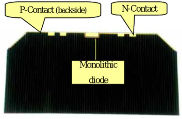
(2) Trans. JSASS Space Tech. Japan Vol. 7 (2009). Design A is categorized as a Schottky diode. A by-pass function is applied between the top junction and the middle junction. On the other hand, three junctions are protected by a P/N junction diode in Design B. The MD is grown on the triple junctions shunted by a metal layer. The forward voltage drop of Design B is higher than that of Design A.. Electrostatic discharge (ESD) is often observed around the stress-relief loop of the interconnectors in the ground testing of a solar array coupon panel, as shown in Fig.3. The root of the interconnector is surrounded by a charged insulator (coverglass), conductor (interconnector and/or solar cell), and insulator (adhesives and/or insulation layer), which form a so-called “triple-junction”, where three materials with different electrical conductivity meet. The electric filed at the triple junction is intensified by charging the nearby insulator, and ESD is easily generated compared to the other areas. The discharge sometimes grows to a continuous discharge between adjacent cells, and then, the insulation layer under the solar arrays is damaged. This is considered as one of the mechanisms of solar array failure in orbit. 1) The initial discharge around the interconnectors is called a “primary discharge”. The primary discharge can degrade the performance of solar cells by decreasing their shunt resistance. 2) From the above standpoint, the MD function faces the primary discharge in orbit when spacecraft charging occurs. Therefore, the resistance of MD cells against primary discharge should be evaluated by ESD testing before being used for flight solar arrays. Clevenger et al. investigated the resistance of the MD function against rush current by a conventional electrical circuit with capacitance and switching. 3) The purpose of the present paper is to report the threshold of MD function degradation obtained in laboratory testing that simulates in-orbit charging situations using solar array coupon panels, and discuss its suitability for flight solar arrays.. Metal (N-contact) Top cell n Top cell p Buffer Middle cell n Middle cell p Metal (Contact) Buffer Bottom cell n. Bottom cell p Metal (P-contact). Cross-section of MD function in Design A. Metal (Contact). Metal (N-contact) Top cell n Top cell p Buffer Middle cell n Middle cell p Buffer Bottom cell n. p GaAs n GaAs n+ GaInP n+ GaAs. Top cell n Top cell p Buffer Middle cell n Middle cell p Buffer Bottom cell n. Bottom cell p Metal (P-contact). Cross-section of MD function in Design B Fig.4. Two design types of MD for ESD testing.. Fig.3. Image of the typical discharge on a solar array. 3.. ESD Testing for MD Cell Coupon. 3.1. Characteristics of MD function at primary discharge 2.. Design of MD Function for ESD Testing To understand the degradation characteristics of MD function by primary discharge, an ESD test coupon panel was prepared. To see the difference between the two MD. Two types of MD solar cells were available for our ESD test. Figure 4 shows their schematics. 12.
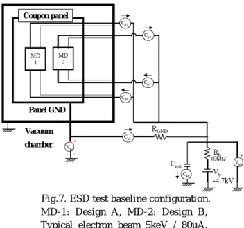
(3) Y. NOZAKI et al.: ESD Ground Testing of Triple-Junction Space Solar Cells with Monolithic Diodes. function designs, the same silver interconnector and same cover-glass (CMG-100 with AR coating) were assembled on both types of MD cells and bonded on the same coupon substrate. Figure 5 shows the coupon panel for ESD testing. The left module is Design A (MD1) CICs (cover-integrated solar cells) and the right CICs are Design B (MD2). Each cell has the same size.. The C ext in Fig.7 can control the energy level of the primary discharge. At first, 2µF with resistor and inductance was connected in series, but then it became difficult to record the discharge waveform because of their complexity. Therefore, C ext was changed from 2µF to 160nF without resistor and inductance. Coupon panel. Panel GND Vacuum chamber. Fig.7. ESD test baseline configuration. MD-1: Design A, MD-2: Design B, Typical electron beam 5keV / 80µA.. Fig.5. Coupon panel for ESD Testing. The test coupon was set in a space vacuum chamber as shown in Fig.6. The length and diameter of the chamber are 1.2m and 1.0m, respectively. An electron gun, mounted on top of the chamber, irradiates the test coupon with an electron beam. An infrared camera is set in front of the upper window to monitor discharge on the coupon panel. Figure 7 shows the electrical connection in the ESD test. Two solar arrays were connected together and were negatively biased at -4.7kV by a DC power supply during the test to simulate the inverted potential gradient conditions. The coupon substrate was insulated from the chamber, and was also negatively biased along with the solar cells. This is a typical ESD test configuration of a solar array coupon for a geo-synchronous earth orbit (GEO) environment. 4). The electron beam was applied to both MD1 and MD2 solar arrays on the coupon panel under the inverted potential gradient condition for 20 hr. Voltage current (V-I) curves of each solar array were measured by a solar simulator using a Xenon lamp before and after ESD testing to precisely estimate the degradation of electrical performance of the MD solar arrays. During the test, 74 discharges were observed. 31 discharges occurred on the MD1 solar array and 43 discharges occurred on the MD2 solar array. Typical discharge images are shown in Fig.8. The left photo shows the discharge on the MD1 solar array. From the illuminated image, it can be understood that the discharge current flew from the interconnector to the negative end of the array through the solar cell. In the right photo, the discharge passed through the entire MD2 solar array from the negative end. After ESD testing, the V-I curve of MD2 measured by a solar simulator and the result showed significant degradation. The maximum power of the MD2 solar array measured after ESD testing was about 62% of its initial power. The maximum discharge current was more than 60 amperes. Both by-pass function and solar array junctions were damaged. On the other hand, the electrical output of the MD1 array did not change. The maximum discharge current was less than 30 amperes. The discharge current of MD1 was smaller probably because of its higher impedance of series connected bottom junction cell as shown in Fig. 4. There is a possibility that this prevented the degradation of. Fig.6. MD cell array coupon in the test chamber. 13.
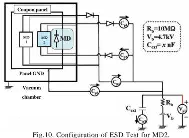
(4) Trans. JSASS Space Tech. Japan Vol. 7 (2009). electrical performance. Coupon panel. Panel GND Vacuum. Fig.8. Typical discharges of MD1 and MD2.. chamber. 3.2. Threshold of degradation of MD function Fig.10. Configuration of ESD Test for MD2. Typical electron beam 5keV / 80µA.. To identify the threshold discharge energy to affect the by-pass function, one more coupon panel was prepared. To generate primary discharges only on the target array, another solar array was covered with a Mylar sheet. In Fig.9, MD2 was exposed to an electron beam to generate primary discharges on the MD2 array. To control the direction of the discharge current, two diodes were added between the solar arrays and Cext / power supply as shown in Fig.10. As electron beam (4keV / between 40 and 100µA) was applied on the surface of the coverglass of the MD2 solar array. The coupon panel was kept at -4.7kV to generate an inverted potential gradient condition on the solar array. C ext was increased from 10nF till when the cell dark V-I curve changed.. Up to Cext of 60.3nF, the dark V-I curve of the array circuit measured after every discharge did not change. Five discharges occurred in the case of Cext=60.3nF, and the maximum discharge current was 50.3 amperes. There were no changes in the dark V-I curves. However, when Cext was raised to 73.7nF, the dark V-I curve changed after the third discharge. The primary discharge at the third cell from the positive end of the string was observed as shown in Fig.11. The peak discharge current was 37.5 amperes as shown in Fig.12. The duration was 30µsec and the discharge energy was 0.8J (350µC). The dark V-I curves measured before and after the discharge are shown in Fig.13. In the figure, the cell V-I represents the voltage-current curve of the TJ solar cell and the MD V-I stands for the same in the MD function. It became clear that the solar array was damaged by the discharge having the waveform shown in Fig.12.. Fig.9. Coupon panel covered with Mylar sheet. Figure 11 shows the image of a typical discharge of MD2 observed during the ESD test. Due to the extra diodes at the positive and negative lines, the discharge current passed through the by-pass function only.. Fig.11. Typical discharge on a MD2 solar array. 14.
(5) Y. NOZAKI et al.: ESD Ground Testing of Triple-Junction Space Solar Cells with Monolithic Diodes. The coupon panel was removed from the test chamber. The V-I curves of the solar array and MD function measured separately indicate that the MD function was damaged. Therefore, 0.8J can be considered as the threshold of discharge energy for the by-pass function of the MD2 solar cell.. Fig.12. Waveform of the third discharge. C ext = 73.7 nF.. After the test on MD2, the Mylar sheet was switched from MD1 to MD2 and an ESD test of the MD1 array was carried out. C ext was varied from 50nF to 150nF during the test, but no degradation of dark V-I curves was observed. The maximum discharge current was 94 amperes, and its duration was more than 20µsec as shown in Fig.14. The calculated energy of the discharge was 650µC, and that was almost double the threshold energy of the degradation on MD2 (Design B). It can be considered that MD1 (Design A) is very strong against primary discharges on a solar array.. Fig.13. Cell V-I and MD V-I before and after the discharge shown in Fig.11.. Fig.14. Image and waveform of discharge on MD1.. 15.
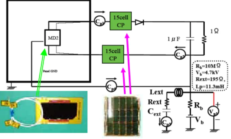
(6) Trans. JSASS Space Tech. Japan Vol. 7 (2009). 3.3. Degradation of MD2 on a realistic solar array To estimate the actual degradation of a MD solar array in orbit, ESD testing of a MD2 solar cell connected to a realistic solar array circuit was conducted. To control the waveform of the primary discharge to simulate predicted discharge on an actual solar array in orbit, resistance and inductance were connected to the external capacitance (C ext ) in series. Figure15 shows a test coupon. The test circuit is shown in Figure16. The solar array for a spacecraft that employs a 50-volt bus system usually consists of about 30 TJ solar cells connected in series to generate 50 volts under any conditions in orbit. So two coupon panels, each coupon with 15 TJ cells, are set outside of the vacuum chamber and connected to the MD2 coupon. As there is no diode in return line on most flight solar arrays, the diode remains on the positive line only. A capacitor and resistor were also inserted between the positive and negative lines to simulate the actual load on the spacecraft as much as possible. The electron beam and bias voltage applied to the test coupon were the same as the ones in the ESD tests described in section 3.1 and 3.2. C ext was varied from 100nF up to 844nF. Inductance and resistance of the external circuit (L ext and R ext ) were selected to make the waveform of the discharge current realistic on a 2.4m by 8m solar array in a GEO environment. 5) V-I curves of the cell and MD were measured before and after every discharge, but no degradation of the curves was observed till C ext =844nF, the energy of the discharge was almost 9.3J (3700µC). The MD2 was degraded by a discharge with energy of 0.8J (350µC) in the previous test, but there was no degradation even at the time of a higher discharge. The difference between the two kinds of tests is the impedance of the discharge circuit that might cause a large modification in the discharge waveform.. Fig.16. Test configuration for a realistic circuit. Typical electron beam 5 keV / 80µA.. Figure 17 shows the discharge and its waveform, when C ext was 844nF. The discharge current flowed through both the positive line and the negative line, because there is no blocking diode in the negative line. The total discharge current was 20 amperes, and 5 amperes passed through MD2. On the actual solar array in orbit, the discharge current originating from the primary discharge caused by the charged coverglass will flow in both directions through the by-pass functions and solar cells. The duration of the discharge was expanded more than 20 times than the discharge observed in the previous tests. The MD function seems to be safe for long discharges, when their peak current is less than 30 amperes. But it is believed that around 0.8J (350µC) is the threshold for the MD function, as the discharge exceeds 30 amperes.. Fig.15. MD2 test coupon for a realistic circuit test.. Fig.17. Waveform of the discharge on MD2. C ext =844 nF. 16.
(7) Y. NOZAKI et al.: ESD Ground Testing of Triple-Junction Space Solar Cells with Monolithic Diodes. The ESD test in Section 3.2 indicated that the threshold of discharge energy for the by-pass function of a MD2 solar cell is 0.8J. A previous experiment showed that the threshold discharge energy was 0.015J for a crystalline silicon cell and 0.053J for a CIGS cell. 6) Therefore, it is considered that the MD functions tested this time have enough resistance for primary discharge.. A 2.4m by 8m with dimensions of solar array using TJ solar cells can generate several kW in orbit. Based on the results of the ground testing in this section, the current of the primary discharge will pass through both the MD function and solar cells, and then the peak current will be limited by the resistance of the plasma generated by the primary discharge. This means all of the charged energy will not rush into the MD function. Therefore, even the MD2 on an actual solar array does not degrade at a discharge of 9.3J, and both types of MD solar cells reported in this paper will not degrade by the rush current of the primary discharge on a several-kW class flight solar array in orbit.. 5. Conclusion The threshold energy of the primary discharge for the degradation of MD function was evaluated. Two types of MD design were tested, and it was found that the resistance for arcing is different. Based on ground experiments, both designs are available for a several-kW class solar array in light of the degradation caused by the primary discharge on actual flight solar arrays in orbit.. 4. Discussion of Test Results To identify the broken portion of MD2, an electro luminescence (EL) image of the damaged cell mentioned in Section 3.2 was observed. A DC current of 0.3A was injected to the damaged MD from its anode to the cathode, and the luminescence was observed using an infrared camera. As shown in Fig.18, a dark area was observed. On the other healthy MD cells, the dark portions were not observed. As the bright area is the EL of the GaAs P-N junction (MD function), the current in the dark area did not pass through GaAs and it was shunted by the leak resistance generated by ESD. Therefore, it can be considered that the area was damaged by the rush current of the primary discharge and the edge of the diode junction became the leakage path for the applied DC current.. Acknowledgments The authors would like to thank Dr. S. Hosoda, Dr. T. Okumura, and Mr. J. Ninomiya for their support in conducting ESD tests.. References MD function. 1) Dark spot. 2). MD function Test wire. 3). 4). Fig.18. EL image around a damaged MD function. (Observed on MD2 after the test discussed in Section 3.2.). 5). Because the structure of MD2 (Design B) is complex, as shown in Fig.4, MD was sensitive to the rush current. On the other hand, MD1 (Design A) has a simple structure made by a single metal layer and negative semiconductor layer. This might be one of the reasons that MD1 was not destroyed by the primary discharge up to about 100 amperes / 650µC.. 6). 17. Snyder, D., Ferguson, D., Vayner, B. and Galofaro, T. : New Spacecraft-Charging Solar Array Failure Mechanism, 6 th Spacecraft Charging Technology Conference, November, 1998. Imaizumi, M. : What Is the Happening on Space Solar Cells? , 1 st Int’l Workshop on Electrostatic Discharge Effects, November, 2006. Clevenger, B., Hise, L., Newman, F., Aiken, D. and Sharps, P. : Evaluation of ESD Susceptibility of Solar Cells with a Monolithic Bypass Diode, 32 nd PVSC-WPEC, Hawaii, 2006. Toyoda, K., Matsumoto, T., Cho, M., Nozaki, Y. and Takahashi, M. : Power Reduction of Solar Arrays by Arcing under Simulate GEO Environment, Journal of Spacecraft and Rockets, 41, 5(2004), pp 854-861. Masui, H., Ose, T., Toyoda. K. and Cho, M. : Sustained Arc Test for Formulating Design Guideline of Solar Array Panel, 26 th ISTS, 2008-r-2-18, 2008. Okumura, T., Hosoda, S., Kim, J., Toyoda, K., Cho, M. and Kawakita, S. : ESD Test on Cu(In, Ga)Se2 Thin-film Solar Cell in Simulated LEO Environment, 25 th ISTS, 2006-s-17, 2006..
(8)
図
関連したドキュメント
A three-stage room thermostat is modeled to output three on/off control functions that can be used to control a system having a solar heat source, an auxiliary heater, and a
Shi, “The essential norm of a composition operator on the Bloch space in polydiscs,” Chinese Journal of Contemporary Mathematics, vol. Chen, “Weighted composition operators from Fp,
We use the monotonicity formula to show that blow up limits of the energy minimizing configurations must be cones, and thus that they are determined completely by their values on
One important application of the the- orem of Floyd and Oertel is the proof of a theorem of Hatcher [15], which says that incompressible surfaces in an orientable and
The theory of log-links and log-shells, both of which are closely related to the lo- cal units of number fields under consideration (Section 5, Section 12), together with the
We relate group-theoretic constructions (´ etale-like objects) and Frobenioid-theoretic constructions (Frobenius-like objects) by transforming them into mono-theta environments (and
The theory of log-links and log-shells, which arise from the local units of number fields under consideration (Section 5), together with the Kummer theory that relates
The theory of log-links and log-shells, both of which are closely related to the lo- cal units of number fields under consideration (Section 5, Section 12), together with the
