Solution-processed anthradithiophene-PCBM p-n junction photovoltaic cells fabricated by using the photoprecursor method
3
0
0
全文
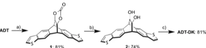
(2) 50. Scheme 2 Synthesis of ADT-DK. Reagents and conditions: a) vinylene carbonate, xylenes, autoclave, 180 oC, 3 days; b) 4M NaOH, THF, reflux, 2 h; c) TFAA, DMSO, DIPEA, dry-CH2Cl2, –60 oC, 1.5 h. 5. 10. 15. 20. 25. 30. absorption of the diketone moiety. The photoreaction of ADTDK to ADT was monitored by the change in UV–vis absorption (ESI†, Figure S2). A toluene solution of ADT-DK (0.2 mg in 10 ml) was bubbled with argon, and the solution was irradiated by a 500 W xenon lamp through a monochrometor (lEX = 468 nm, 14.9 mW cm –2). The reaction finished in 17.5 min in this case. The photoreaction of ADTDK was also performed in a spin-coated thin film, and the complete conversion to ADT was confirmed by IR spectra (ESI†, Figure S3); namely, the C=O stretching band at 1730 cm –1 disappeared after irradiation by a blue LED lamp for 30 min in a glove box. The ionization potential of thus obtained ADT film was determined to be 5.1 eV by photoelectron spectroscopy (ESI†, Figure S4). This value is comparable with that obtained for a thin film of directly deposited anthra(2,3b:6,7-b′)dithiophene (anti-ADT).19b Solution-processed p–n junction devices based on photogenerated acene and PC 61BM were typically fabricated as follows (Figure 1): After spin-coating of PEDOT:PSS on ITO, PDK or ADT-DK in CHCl3 (5 mg ml–1) was spin-coated at 800 rpm for 30 sec then irradiated by a blue LED at rt for 30 min. On top of that, PC 61BM in CHCl3 (10 mg ml–1) was spin-coated at 800 rpm for 30 sec, then Ca (10 nm) and Al (80 nm) were sequentially deposited. This process affords devices with a structure described as [ITO / PEDOT:PSS (30 nm) / Acene (40 nm) / PC 61BM (40 nm) / Ca (10 nm) / Al (80 nm)].. 55. 60. acene PCBM(mg ml-1) / PEN ADT PEN ADT ADT ADT ADT. 65. 75. Figure 1 Schematic diagram of fabrication of p-n junction OPV devices.. 40. 45. The photovoltaic performance of the obtained devices is summarized in Figure 2 and Table 1. The device based on PEN and PC 61BM showed a PCE of 0.25% (short circuit current density, JSC = 0.80 mA cm –2; open circuit voltage, V OC = 0.52 V; fill factor, FF = 0.59). By replacing PEN with ADT, PCE increased by approximately three times to 0.74% (Jsc = 1.91 mA cm –2, Voc = 0.61 V and FF = 0.64). Employment of PC 71BM instead of PC 61BM led to a considerably higher Jsc value,18 resulting in an even higher PCE of 1.54% (Jsc = 3.46 mA cm –2; V OC = 0.67 V; FF = 0.66). In this case again, the ADT-based device showed a PCE approximately three times higher than that of the PEN-based counterpart (PCE = 0.44, Jsc = 1.56 mA cm –2; V OC = 0.53 V; FF = 0.53). To evaluate the influence of n-layer thickness, a few ADT– PC 71BM devices were additionally prepared using PC 71BM solutions of different concentrations from 5 to 20 mg ml–1, 2 | Journal Name, [year], [vol], 00–00. Figure 2 (a) I–V curves for PEN–PC61BM (black lines) and ADT– PC61BM (red lines) devices; (b) I–V curves of PEN–PC71BM (10 mg ml– 1 ) (black lines) and ADT–PC71BM (red lines) devices; larger circles: under AM 1.5G illumination; smaller circles: in the dark. Table 1 Performance of the acene–PCBM p–n junction OPV devices.. 70. 35. which corresponds to the resulting film thickness of 13–116 nm. (The film thicknesses were summarized in Table S1 in ESI†) The best performance was achieved at 10 mg ml–1 concentration (40 nm film thickness). When the PC 71BM film is thicker, Jsc decreased because of the higher resistance of the film. With a thinner PC 71BM film, Voc decreased because of the higher leak current.. 80. 85. 90. PC61BM(10) PC61BM(10) PC71BM(10) PC71BM(5) PC71BM(10) PC71BM(15) PC71BM(20). Jsc / mA cm-2 0.80 1.91 1.56 2.08 3.46 2.49 1.82. Voc /V 0.52 0.61 0.53 0.49 0.67 0.66 0.64. FF 0.59 0.64 0.53 0.53 0.66 0.58 0.48. PCE Rs / Rp /% ohm cm-2 ohm cm-2 0.25 57 2416 0.74 31 5052 0.44 45 1015 0.53 42 888 1.54 24 13336 0.95 69 2522 0.56 194 3116. The incident photon-to-current conversion efficiency (IPCE) curves and the UV–vis spectra of the acene–PCBM (10 mg ml–1) devices are shown in Figure 3. By using PC 71BM, the absorbance of the multilayer films in visible region increased by 1.5 to 2 times compared to the cases when PC 61BM was used.20a Furthermore, the ADT device showed higher performance than the PEN device in each case, although the absorption abilities are comparable to each other. The slightly higher V OC of the ADT device is attributed to the deeper HOMO level of ADT (5.1 eV) compared to PEN (5.0 eV). The photocurrent in reverse voltage (Figure 2) was nearly constant in the ADT device, whereas it increases in the PEN device with increasing reverse voltage, which is reflected in the higher FF, lower series resistance (Rs), and higher parallel resistance (Rp) in the ADT device. This difference indicates that the p-layer based on ADT has higher charge extraction ability; i.e., higher charge mobility. To check the film structures of PEN and ADT prepared by photoconversion, X-ray diffraction pattern of the films were measured (ESI†, Figure S5). For the PEN film, a peak corresponding to a d-space of 15.1 Å was observed, suggesting the edge-on arrangement of PEN molecules.21 On the other hand, the ADT film gave a featureless trace without any recognizable peaks. This implies that the randomly oriented ADT film is more suitable for charge extraction in the device, compared to the PEN-based film with the edge-on arrangement having less overlap of p-orbitals along the vertical direction.22. This journal is © The Royal Society of Chemistry [year].
(3) 0.1028, GOF = 1.086. CCDC 955408 contains the supplementary crystallographic data. 1 2. 3. 4. 5. 10. 15. 20. 25. 30. Figure 3 (a) IPCE curves of [ITO / PEDOT:PSS / acene / PCBM / Ca / Al] and (b) absorption spectra of the same active layer films on ITO / PEDOT:PSS without the Ca and Al layers: PEN / PC61BM (black open circles for (a); black broken line for (b)); ADT / PC61BM (red open circles for (a); black red line for (b)); PEN / PC71BM (black closed circles for (a); black solid line for (b)); ADT / PC71BM (red closed circles for (a); red solid line for (b)). The concentration of PCBM solutions is 10 mg ml–1.. Bulk heterojunction devices with acenes as p-type and PC 61BM as n-type materials were also eveluated; however, the PCE values were less than 0.1% with significantly low Jsc values. Considering the high crystallinity of PEN and ADT, the well-mixed i-layers might not be formed in combination with PC 61BM. In summary, we were successful to prepare p–n heterojunction solar cells based on ADT and PCBM via the photoprecursor method for the first time. The PCE of the best performed ADT–PC 71BM device is 1.54%, which is a significant improvement from the 0.25% PCE obrained with our prototype PEN–PC 61BM device prepared by the same method. The results clearly demonstrate that the photoprecusor method makes hardly soluble organic semiconductors such as ADT well compatible with solutionbased deposition techniques. In addition, the photoprecursor approach enables the formation of multilayer structures by solution processes. These achievements pave the way to a widely applicable methodology for the construction of sophisticated multilayer structures (e.g., p–i–n type triplelayer structures) by solution processes. Further research along these lines is underway.. 5. 6 7. 8 9 10 11 12 13 14 15. 16. Notes and references a. 35. 40. 45. Graduate School of Materials Science, Nara Institute of Science and Technology, 8916-5, Ikoma, Nara 630-0192, Japan. Fax: +81-743-726042; Tel: +81-743-72-6041; E-mail: [email protected] b Department of Electrical Devices, Graduate School of Science and Engineering, Yamagata University, Yonezawa 992-8510, (Japan), Fax: (+81)238-26-3713, E-mail: [email protected] c Graduate School of Science and Engineering, Ehime University, Matsuyama 790-8577, Japan d CREST, JST, Chiyoda-Ku, Tokyo 102-0075, Japan † Electronic Supplementary Information (ESI) available: [details of any supplementary information available should be included here]. See DOI: 10.1039/b000000x/ ‡ Crystallographic data for ADT-DK: C20H10O2S2, M = 346.42, orthorhombic, space group Fdd2 (#43), a = 27.54611), b = 33.092(13), c = 6.766(3) Å, V = 6156(4) Å3, T = 100 K, Z = 16, R1 = 0.0448, wR2 =. This journal is © The Royal Society of Chemistry [year]. 17 18 19 20 21 22. a) M. Mas-Torrent and C. Rovira, Chem. Soc. Rev., 2008, 37, 827. b) J. E. Anthony, Angew. Chem. Int. Ed., 2008, 47, 452. c) A. R. Murphy and J. M. J. Fréchet, Chem. Rev., 2007, 107, 1096. a) C. Duan, F. Huang, and Y. Cao, J. Mater, Chem., 2012, 22, 10416. b) H. Zhou and W. You, Macromolecules, 2012, 45, 607. c) P.-L. T. Boudreault, A. Najari and M. Leclerc, Chem. Mater, 2011, 23, 456. d) C. L. Chochos and S. A. Choulis, Prog. Polym. Sci., 2011, 36, 1326. e) Y.-J. Cheng, S.-H. Yang and C.-S. Hsu, Chem, Rev., 2009, 109, 5868. f) J. Chen and Y. Cao, Acc. Chem. Res., 2009, 42, 1709. g) Y. Liang and L. Yu, Acc. Chem. Res., 2009, 42, 1227. a) A. Mishra and P. Bauerle, Angew. Chem. Int. Ed., 2012, 51, 2020. b) Y. Lin, Y. Li and X. Zhan., Chem. Soc. Rev., 2012, 41, 4245. c) B. Walker, C. Kim. and T.-C. Nguyen., Chem. Mater., 2011, 23, 470. d) F. Würthner and K. Meerholz, Chem. Eur. J., 2010, 16, 9366. a) D. Gebeyehu, M. Pfeiffer, B. Maennig, J. Drechsel, A. Werner and K. Leo, Thin Solid Films, 2004, 451/452, 29. b) K. Suemori, T. Miyata, M. Yokoyama and M. Hiramoto, Appl. Phys. Lett., 2005, 86, 063509. c) Y. Matsuo, Y. Sato, T. Niinomi, I. Soga, H. Tanaka and E. Nakamura, J. Am. Chem. Soc., 2009, 131, 16048. a) P. T. Herwig and K. Müllen, Adv. Mater., 1999, 11, 480. b) A. Afzali, C. D. Dimitrakopoulos and T. L. Breen, J. Am. Chem. Soc., 2002, 124, 8812. c) J. Xiao, H. M. Duong, Y. Liu, W. Shi, L. Ji, G. Li, S. Li, X.-W. Liu, J. Ma, F. Wudl and Q. Zhang, Angew. Chem. Int. Ed., 2012, 51, 6094. M. Watanabe, K.-Y. Chen, Y. J. Chang and T. J. Chow, Acc. Chem. Res., 2013, 46, 1606. And references cited therein. a) T. Akiyama, A. Hirao, T. Okujima, H. Yamada, H. Uno and N. Ono, Heterocycles, 2007, 74, 835. b) A. Hirao, T. Akiyama, T. Okujima, H. Yamada, H. Uno, Y. Sakai, S. Aramaki and N. Ono, Chem. Commun., 2008, 4714. S. Ito, T. Murashima, H. Uno and N. Ono, Chem. Commun., 1998, 1661. A. R. Murphy, J. M. J. Fréchet, P. Chang, J. Lee and V. Subramanian, J. Am. Chem. Soc., 2004, 126, 1596. J. S. Zambounis, Z. Hao, A. Iqbal, Nature, 1997, 388, 131. T. L. Chen, J. J.-A. Chen, L. Catane and B. Ma, Org. Electron., 2011, 12, 1126. E. D. Głowacki, G. Voss, K. Demirak, M. Havlicek, N. Sünger, A. C. Okur, U. Monkowius, J. Ga˛siorowski, L. Leonat and N. S. Sariciftci, Chem. Commun., 2013, 49, 6063. H. Yamada, T. Okujima and N. Ono, Chem. Commun., 2008, 2957. H. Yamada, Y. Yamashita, M. Kikuchi, H. Watanabe, T. Okujima, H. Uno, T. Ogawa, K. Ohara and N. Ono, Chem. Eur. J., 2005, 11, 6212. a) J. H. Edwards and W. J. Feast, Polymer, 1980, 21, 595. b) L. H. Nguyen, S. Günes, H. Neugebauer, N. S. Sariciftci, F. Banishoeib, A. Henckens, T. Cleij, L. Lutsen and D. Vanderzande, Sol. Energy Mater. Sol. Cells, 2006, 90, 2815. a) J. Strating, B. Zwanenburg, A. Wagenaar and A. C. Udding, Tetrahedron Lett., 1969, 10, 125. b) R. Mondal, B. K. Shah and D. C. Neckers, J. Am. Chem. Soc., 2006, 128, 9612. c) C. Tönshoff and H. F. Bettinger, Angew. Chem. Int. Ed., 2010, 49, 4125. d) references cited in ref 13. K. Nakayama, C. Ohashi, Y. Oikawa, T. Motoyama and H. Yamada, J. Mater. Chem. C., 2013, 1, 6244. K. Takimiya, S. Shinamura, I. Osaka and E. Miyazaki, Adv. Mater., 2011, 23, 4347. a) J. G. Laquindanum, H. E. Katz and A. J. Lovinger, J. Am. Chem. Soc., 1998, 120, 664. b) M. Nakano, K. Niimi, E. Miyazaki, I. Osaka, K. Takimiya, J. Org. Chem., 2012, 77, 8099. a) M. M. Wienk, J. M. Kroon, W. J. H. Verhees, J. Knol, J. C. Hummelen, P. A. van Hal and R A. J. Janssen, Angew. Chem. Int. Ed., 2003, 42, 3371. b) Karl Leo, Appl. Phys. Lett., 2009, 94, 223307. C. D. Dimitrakopoulos and P. R. L. Malenfant, Adv. Mater., 2002, 14, 99. Preliminary space charge limited current measurements gave hole mobilities along the vartical direction of 3.41 × 10⁻⁴ and 1.06 × 10⁻⁴ cm2 V–1 s–1 in ADT and PEN, respectively. See ESI†, Figure S6.. Journal Name, [year], [vol], 00–00 | 3.
(4)
図
関連したドキュメント
As an application, we present in section 4 a new result of existence of periodic solutions to such FDI that is a continuation of our recent work on periodic solutions for
In [6], two-dimensional convex and nonconvex geometries have been considered and some solution methods for the discrete heat equation, for example, the conjugate gradient method,
Jin [21] proved by nonstandard methods the following beautiful property: If A and B are sets of natural numbers with positive upper Banach density, then the corresponding sumset A +
The seasonal variations of the vertical structure of temperature, salinity and geostrophic velocity at latitude 6 ° N in the Bay of Bengal have been investigated, using the
1月 2月 3月 4月 5月 6月 7月 8月 9月 10月 11月 12月.
6月 7月 8月 10月 11月 5月.
1月 2月 3月 4月 5月 6月 7月 8月 9月10月 11月 12月1月 2月 3月 4月 5月 6月 7月 8月 9月10月 11月 12月1月 2月 3月.
2月 1月 12月 11月 10月 9月 8月 7月
