Synthesis Using Cu(Ti) Alloy Films for Self-Forming Functionality in Electronic Devices
7
0
0
全文
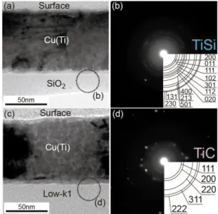
(2) Synthesis Using Cu(Ti) Alloy Films for Self-Forming Functionality in Electronic Devices used for making Cu interconnects, as shown in Fig. 1. Digging a groove so-called via and trench is the first, and then Cu film is electrochemically deposited, and finally chemical-mechanical polishing was conducted. In fabrication of Cu interconnects, large resistance-capacitance (RC) delay and poor device reliability have been critical issues as the device feature size has reduced to nanometer scale1). In the RC delay, resistivity increase due to barrier layers is becoming significant with the reduction in line width of the Cu interconnects. Moriyama et al.2) and Shimada et al.3) reported that significant resistivity increase is observed when the line width decrease to smaller than 100 nm and a very thin barrier layer (< 5 nm) is required for the interconnects with a line-width of ~ 45 nm and an average grain size of ~ 450 nm to achieve an effective interconnect resistivity of less than 4 μΩ-cm (Fig. 2). Thus, our goal is how to make a thin barrier and large-grained Cu interconnects.. atoms in the Cu(Ti) alloy seeds can react with many kinds of dielectrics such as SiO2, SiOC, SiCO, and SiCN, resulting in formation of SFB with different composition11). However, the technique using a Cu(Ti) alloy seed has not been applied to dual-damascene interconnects. In this paper, we firstly show characterization of Ti-based SFB using transmission electron microscope (TEM)/energy dispersive X-ray spectroscopy (EDS), X-ray photoelectron spectroscopy (XPS), and Rutherford backscattering spectrometry (RBS), and examples applied Ti-based SFB to the Cu dual-damascene interconnect for 45-nm node of ULSI. 2. Ti-based SFB characterization 2.1 Identification of Ti-based SFB using XPS TEM/selected area diffraction (SAD) observation showed that the Ti-based SFB consisted of crystalline Ti compounds (TiC, TiSi or TiN)9-12). Figure 4 shows cross-sectional TEM images and SAD images taken from an area marked with a broken circle in the TEM images for an annealed Cu(Ti)/SiO2 (Fig. 4(a)) and Cu(Ti)/Low-k1 (Fig. 4(c)) samples. Thin Ti-based SFB layers formed at the interfaces between a Cu(Ti) alloy film and dielectrics. They consisted of polycrystalline TiSi on SiO2 (Fig. 4(b)) and TiC on Low-k1 (Fig. 4(d)). The kinds of the Ti compounds formed in the Ti-based SFB depended on the kinds of dielectrics. The thickness, dielectric constants, and compositions of the dielectrics are shown in Table 1. The TEM/SAD observation and SIMS analyses suggested that the Ti-based SFB consisted of amorphous Ti oxides (TiOx) as well as the crystalline Ti compounds. Although the barrier structure and amorphous phases in the barrier were not directly identified by the TEM/SAD observation and SIMS analyses, an XPS. Fig. 2 Theoretical resistivities as a function of grain sizes and effective resistivities as a function of barrier thickness calculated using the MS model with P=0 and R=0.5 for the Cu interconnects 3). Various methods have been reported to reduce the volume of barrier layers in Cu interconnects by fabricating an ultra thin barrier 4-12). Formation of a thin barrier layer by annealing Cu alloy seeds at elevated temperatures is conventionally called a self-formed barrier (SFB) technique. The Cu alloy films with various solutes (Mg, Ti, Al, Cr, etc.) were extensively investigated for the possibility of the self-formation of the passivation layers13-21), and those with Mn7,8) and Ti for SFBs9-12). The SFB technique is essential for reaction of solute atoms with dielectrics as shown in Fig. 3. The Ti. Fig. 4 Cross-sectional TEM images of the (a) Cu(Ti)/SiO2 and (c) Cu(Ti)/Low-k1 after annealing at 600°C for 2h in Ar, respectively. (b) and (d) are SAD images taken from the areas marked with broken circles in (a) and (c), respectively.. Fig. 3 Schematic illustrations of Ti-based self-formed barrier (SFB) synthesis using Cu(Ti) alloy films annealed at elevated temperature and its TEM/EDS mapping result 9).. 38.
(3) Transactions of JWRI, Vol.43 (2014), No. 2 Table 1 Dielectric constants (k) and thickness of dielectric layers and their C, O, Si and N concentration (at.%) 12). Dielectrics. k. th-SiO2 Low-k1 Low-k4 SiCN. 3.9 3.0 2.6 4.8. t (nm) 100 440 450 200. C (at.%) 17.0 ~14 21.4. O (at.%) 66.7 24.9 ~29 0.5. Si (at.%) 33.3 18.8 ~18 25.0. N (at.%) 12.8. technique with simultaneous Ar etching was employed to investigate the structure of the Ti-based SFB and its compositions systematically with dielectrics. Figure 5(a) shows typical elemental depth profiles of the Cu(Ti)/SiO2 sample after annealing in ultrahigh vacuum (UHV) at 600°C for 2h obtained by simultaneous Ar etching and XPS measurements. Ti segregation was observed around etch times between 18000s and 25000s (at the interface), where oxygen and Si atoms were also detected. To identify composition of the Ti-based SFB, XPS measurements around the binding energies of Ti 2p, C 1s, Si 2p, and N 1s were performed. Portions of the XPS profiles around the binding energies of Ti 2p (460 eV22,23)) obtained from the middle of Ti-based SFB (etch time of about 21600 s) are shown in Fig. 5(b). They varied with dielectrics and were fitted by the sum of the XPS profiles of TiO/TiC, TiO2, Ti2O3, and a background. Similarly, XPS profiles around the binding energies of C 1s, Si 2p, and N 1s were fitted. Based on the fitting, volume fractions of TiC, TiSi, TiN, TiO2, Ti2O3, and TiO phases were determined by a ratio of each peak area to sum of peak areas. Figure 6 shows depth dependence of composition of the Ti-based SFB in the annealed Cu(Ti)/dielectrics samples. In the Cu(Ti)/SiO2 sample, Ti-based SFB mainly consisted of Ti oxides. The Ti oxides were in amorphous state, since crystalline Ti oxides were not detected by TEM/SAD analyses (Fig. 4(a)). Similarly, Ti-based SFBs in the other samples (Low-k1, Low-k4, SiCN) consisted of a large amount of amorphous Ti oxides (50~75%), as shown in Fig. 6. The crystalline TiC was observed in the annealed Cu(Ti)/Low-k1 and Cu(Ti)/SiCN samples, and amorphous TiC was observed. Fig. 6 Depth dependence of volume fractions of Ti compounds in the Ti-based SFB formed on the SiO2, Low-k4, Low-k1, and SiCN layers after annealing in UHV at 600°C for 2h 12). in the annealed Cu(Ti)/Low-k4 sample. TiN observed in the annealed Cu(Ti)/SiCN sample was in the amorphous state. The volume fractions of TiC and TiN were estimated to be about 20%, and both phases occupied a small part of the Ti-based SFB. While, a small amounts of TiSi was observed in the Cu(Ti)/SiO2 and Cu(Ti)/Low-k4 samples, but not observed in the other samples12). This is in good agreement with the previous study11). The crystalline Ti compounds such as TiC and TiSi tended to form beneath the Cu(Ti) alloy films. Some SAD patterns obtained in Cu(Ti)/Low-k1 and Cu(Ti)/SiCN samples showed that orientation relationship between crystalline TiC and Cu grains (not shown). This is one of the evidences that TiC formed beneath the Cu(Ti) alloy films. On the other hand, the amorphous phases such as TiOx tended to form above the dielectric layers. The amorphous phases were believed to form continuously above the dielectric layers, and play an important role to prevent Cu diffusion into the dielectrics. 2.1 Ti-based SFB growth characterized by RBS Growth of the Ti-based barrier was characterized using Rutherford backscattering spectroscopy (RBS). Figure 7 shows RBS spectra of the annealed Cu(Ti)/low-k1 samples with various Ti contents. Ti segregation was observed at the interface in all samples. Fig. 5 (a) A XPS depth profile of the Cu(Ti)/SiO2 sample after annealing in UHV at 600°C for 2h and (b) portions of XPS spectra around the binding energies of Ti 2 obtained from the middle of the Ti-based SFB formed in Cu(Ti)/dielectrics after annealing in UHV at 600°C for 2h 12).. Fig. 7 RBS profiles of the Cu(Ti)/Low-k1 after annealing in UHV (a)-(c) at 400°C for various time (t) and (d)-(f) at various temperatures (T) for 2h 24).. 39.
(4) Synthesis Using Cu(Ti) Alloy Films for Self-Forming Functionality in Electronic Devices They were almost similar for all the samples regardless of the kinds of dielectric layers at each initial Ti concentration in the alloy films. The m value estimated at the initial Ti concentration of 1 at.% was a little higher (m=0.22) than those (m=0.15) at 5 at.% and 10 at.%. The similar m values suggest that growth of the Ti-rich interface layers was controlled by a similar mechanism. The m values were around 0.2, lower than 0.5, suggesting that growth of the Ti-rich interface layers is not controlled by lattice diffusion but by grain-boundary and/or interface diffusion. Figure 9(d)-(f) show Arrhenius plots of log n versus 1/T in Cu(Ti)/dielectrics for the inital Ti concentrations of 1 at.%, 5 at.%, and 10 at.%, respectively. These show a linear relationship, which suggests that the formation of the Ti-based SFB was controlled by a thermally-activated process. Slopes of the log n versus 1/T lines at the initial Ti concentration of 1 at.% were a little smaller than those at 5 at.% and 10 at.%, which were similar. This corresponds to the behaviors indicated in Figs. 9(a)-(c). The initial Ti concentration at 1 at.% is insufficient to induce reaction of the Ti atoms with the dielectric layers. Activation energies, E, were estimated from the slopes of the log n versus 1/T lines. The E values were plotted as a function of C concentration of the dielectric layers (Fig. 10(a)). The E values at the initial Ti concentration of 5 at.%Ti and 10 at.%Ti were similar. The E values for the samples consisting of dielectric layers containing carbon (except SiO2) tended to decrease with decreasing C concentration (decreasing k), and those without carbon (SiO2) were much higher than others. This indicates that the reaction of the Ti atoms in the alloy films with the low-k layers is the most easily thermally-activated process. Also, composition of the dielectric layers is suggested to play an important role in the reaction of the Ti atoms with dielectric layers, and the carbon may be a key element to control the reaction. This is similar to the formation rule of Ti compounds (TiC or TiSi) in the Ti-rich interface layers. The pre-exponential factors, Z, were estimated from intercepts of the slopes in the log n versus log t lines (Figs. 9(a)-(c)) and log n versus 1/T lines (Figs. 9(d)-(f)). The Z values estimated from two different sets of data were the same at each initial Ti concentration and dielectric layer. The Z values the Cu(Ti)/dielectrics after annealing in UHV were plotted as a function of C concentration of the dielectric layers (Fig. 10(b)). This is similar to the E behavior as shown in Fig. 10(a). The pre-exponential factor shows the frequency with which the Ti atoms meet elemental reactants in the dielectric layers. The frequency was low in the samples with low-k, and was high in the samples with SiO2. In consequence, coefficients of the reaction rate (Z·exp(-E/RT)) were insensitive to C concentration in the dielectric layers at the initial Ti concentrations of 5 at.% and 10 at.%. These factors lead to the conclusion that growth of the Ti-based SFB is controlled by chemical reactions, represented by the Z and E values, of the Ti atoms with the dielectric layers, although there are few diffusion processes. Fig. 8 RBS measurement principle and a fitting example of RBS spectrum for Cu(Ti)/Low-k1 after annealing at 400°C for 2h. 24). . Ti content segregated at the interface was estimated based on RBS theory. Figure 8 shows the RBS measurement principle and an example of refinement plots placed upon the RBS spectrum of Cu(Ti)/Low-k1 after annealing at 400°C for 2h24). The estimated molar amount of Ti atoms (n) is consistent with the molar amount of Ti atoms reacted with dielectrics, which follows the reaction formula n = Z·exp(-E/RT) ∙ tm, (1) where Z is a pre-exponential factor and E is the activation energy for the reaction. Figure 9(a)-(c) show plots of log n versus log t for Cu(Ti)/dielectrics with the inital Ti concentrations of 1 at.%, 5 at.%, and 10 at.%, respectively, after annealing in UHV at 400°C. Those exhibit the growth behaviors of the Ti-rich interface layers. The log n values were found to be proportional to the log t values in all the samples, regardless of the initial Ti concentration in the alloy films or the kinds of dielectric layers. The m values were estimated from the slopes of the log n versus log t lines.. Fig. 9 (a)-(c) Plots of log n versus log t for Cu(Ti)/dielectrics after annealing in UHV at 400°C and (d)-(f) Arrhenius plots of log n versus log 1/T for Cu(Ti)/dielectrics after annealing in UHV for 2h 24).. 40.
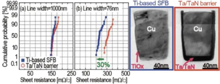
(5) Transactions of JWRI, Vol.43 (2014), No. 2. Fig. 10 (a) Activation energies of E 24) and (b) values of Z of the Cu(Ti)/dielectrics after annealing in UHV as a function of C concentration of the dielectrics.. Fig. 12 Schematics of process flow for Ti-based SFB: after Cu(Ti) and pure-Cu seed deposition, after ECP-Cu deposition, after annealing, after CMP, and interconnect structure after fabrication.. Fig. 11 Schematic illustration of the role of E and Z in reaction of Ti atom in Cu(Ti) alloy with dielectrics. possible in all the samples since the m values suggest that it is controlled by grain-boundary and/or interface diffusion. We believe the activation energy relates the chemical bonding energy in the insulator, and Z value relates the frequency that Ti atoms meet elemental reactants such as O, C, N in the insulators, as shown in Fig. 11. We conclude the growth was controlled by chemical reaction of Ti atoms with the reactants in the insulators.. Fig. 13 Cross-sectional TEM image of trench filled with ECP-Cu using Cu(Ti) alloy seed and EDX analysis around the bottom of trench at the ECP-Cu16). To evaluate influence of the Ti-based SFB on electrical properties of the dual-damascene interconnects, via and line resistance measurements were conducted. Distribution of via resistances using the Ti-based SFB is shown together with that using a conventional Ta/TaN barrier (Fig. 14(a)). The average of via resistance using the Ti-based SFB was reduced to about 30% of that using a Ta/TaN barrier, and its distribution drastically improved. The low via resistance and its narrow distribution was explained by no barrier layer formation at the bottom of via using the Ti-based SFB (Fig. 14(b)). In contrast, high resistance barrier formed at the bottom of via using a Ta/TaN barrier (Fig. 14(c)). The line resistances with a 1000nm-wide trench using the Ti-based SFB were almost similar to that using a Ta/TaN barrier (Fig. 15(a)), but those with 76nm-wide trench using the Ti-based SFB were reduced to about 70% of that using a Ta/TaN barrier (Fig. 15(b)). This indicates that line resistance is dependent on thickness of barrier layers for a narrow line, but this is not for a wide line. Figure 15 (c) and (d) shows cross-sectional TEM images of Cu trenches using. 3. Cu dual-damascene interconnects using a Cu(Ti) alloy seed We applied Ti-based SFB to a dual-damascene structure fabricated using 45nm-node interconnect technology with Cu and SiOCH (low-k) dielectrics. The Ti-based SFB was applied to a M2 layer between M1 and M3 layers, which were fabricated using a pure-Cu seed with a conventional Ta/TaN barrier (Fig. 12) 25). To fabricate the M2 layer, a 15nm-thick Cu(Ti) alloy film was deposited on trench and via patterning substrates using an ionized physical vapor deposition (PVD) method, and similarly a 30nm-thick pure Cu film was deposited on the Cu(Ti) alloy seed. A 600nm-thick Cu film was deposited by an electro-chemically plated (ECP) method, and followed by annealing at 450°C for 1 h in nitrogen ambient and Cu-Chemical Mechanical Polishing (CMP). In the process, a very thin 2 nm-thick Ti-based barrier successfully formed between Cu and an insulator film. Ti atoms segregated only at the barrier region, as shown in Fig. 13.. 41.
(6) Synthesis Using Cu(Ti) Alloy Films for Self-Forming Functionality in Electronic Devices. Fig. 16 (a) Relationship between capacitance and resistance of the Cu dual-damascene interconnects. Cumulative (b) breakdown voltage distribution and (c) failure distribution with a comb structure16).. Fig. 14 (a) Cumulative via resistance distribution with Kelvin structures. Cross-sectional TEM images of via bottom using (b) the Ti-based SFB and (c) the Ta/TaN barrier25).. Fig. 17 Stress induced voiding tests of wide M2 via chain at 200°C for 500h; (a) M1=200 nm, V1=70 nm, M2=1000 nm and (b) M2=1000 nm, V2=70 nm, M3=200 nm16).. Fig. 15 Cumulative sheet resistance distribution of (a) a 1000 nm-wide line and (b) a 76 nm-wide line. Cross-sectional TEM images of trenches using (c) the Ti-based SFB and (d) the Ta/TaN barrier25).. (GB) segregation of X atoms, which prevented vacancy migration through GB26-28). In a case of the Ti-based SFB, Ti atoms were detected in the ECP-Cu films by secondary ion mass spectroscopy (SIMS) analyses (not shown). This suggests that the Ti atoms must be segregated in GB, and improve stress migration reliability.. the Ti-based SFB and a Ta/TaN barrier. Thickness of the Ti-based SFB was thinner than that of the Ta/TaN barrier. Also resistivity increase due to impurity Ti atoms in Cu trenches was negligible, since the Ti atoms in the Cu(Ti) seed layer were almost consumed to form the Ti-based SFB at the wall and bottom of the trenches. Thus, the thin Ti-based SFB contributed to decrease of via and line resistance of Cu dual-damascene interconnects. Figure 16(a) shows relationship between capacitance and resistance of the Cu dual-damascene interconnects using both the Ti-based SFB and Ta/TaN barrier. There was almost no change in capacitance between them, but the resistance using the Ti-based SFB was lower than that using a Ta/TaN barrier. Breakdown voltages between Cu interconnects and time dependent dielectric breakdown (TDDB) endurances using a comb structure are shown in Fig. 16(b) and (c), respectively. The breakdown voltages using the Ti-based SFB were a little bit higher than that using a Ta/TaN barrier, and TDDB endurances were similar. Those indicate that the Ti-based SFB has enough barrier property against Cu diffusion into dielectrics. Figure 17 shows resistance shifts after thermal stress with two kinds of via chain patterns: a wide upper line and a wide lower line. The Ti-based SFB was applied to a wide line for both samples, and a Ta/TaN barrier was applied to other layers. Although the resistance using a Ta/TaN barrier increased after thermal stress for both samples, the resistance shift using the Ti-based SFB was very small. The stress induced voiding (SIV) endurance is well-known to be improved by taking Cu(X) (X is Ti, Al) alloy seeds. This was explained by grain boundary. 4. Cu interconnects on TFT-LCDs using Ti-based SFB This process using Ti as an alloy element can be applied for Cu-interconnect formation in TFT-LCDs. Cu(Ti) alloy films were deposited on glass substrates and subsequently annealed in vacuum at 400°C for 3 h. Resistivity of the annealed Cu(Ti) alloy films was significantly reduced to about 2.8 μΩcm. Tensile strength of the Cu(Ti)/glass interface increased to about 60 MPa after annealing. The low resistivity and excellent adhesion resulted from Ti-based oxide layer formation at the Cu(Ti)/glass interface29, 30). 5. Conclusions (1) Ti-based SFB technique was applied to Cu dual-damascene interconnects and its performances were evaluated TEM and EDX analyses showed that a 2 mm-thick Ti-based SFB was formed along the interface between Cu(Ti) and dielectrics. (2) Resistance of the narrow line and via decreased to about 70% and 30%, respectively. Also distributions of these resistances were drastically improved. The breakdown voltage and TDDB performance showed similar performance, indicating the Ti-based SFB has enough barrier property against Cu diffusion into dielectrics. The SIV reliability was improved by using Ti-based SFB technique.. 42.
(7) Transactions of JWRI, Vol.43 (2014), No. 2. (3) XPS analyses showed that the Ti-based SFB consisted of mainly amorphous Ti oxides. Formation of amorphous or crystalline Ti compounds such as TiC, TiN, TiSi was dependent on the kind of dielectric. Those amounts were lower than that of amorphous Ti oxides. RBS analyses showed that Ti-based SFB growth is controlled by a thermally activated process. The E and Z values decreased with decreasing C concentration in dielectrics, suggesting that the growth is controlled by a chemical reactions of Ti atoms with dielectrics.. 9) 10) 11) 12) 13). Acknowledgements This work was supported by a Grant-in-Aid for Scientific Research from the Ministry of Education, Culture, Sports, Science and Technology (15206069 & 18360324), the Nanotechnology Program on Cu Thin Films from the New Energy and Industrial Technology Development Organization (NEDO) of Japan, Shorai Foundation for Science and Technology (Ito), and Research Fellowships of the Japan Society for the Promotion of Science for Young Scientists (Kohama). Authors would like thank M. Murakami, The Ritsumeikan Trust for advices on the whole study, thank K. Ohmori, K. Mori, and K. Maekawa, Renesas Technology Corp., and T. Ohnishi, Kobe Steel Ltd. for Cu dual-damascene interconnects using a Cu(Ti) alloy seed and thank S. Sonobayashi and Prof. H. Sugimura, Department of Materials Science and Engineering, Kyoto University, for XPS measurements.. 14) 15) 16) 17) 18) 19) 20) 21) 22) 23). References 1) 2) 3) 4). 5) 6) 7) 8). M. T. Bohr, and Y. A. El-Mansy, IEEE T. Electron. Dev., 45 (1998) 620. M. Moriyama, M. Shimada, H. Masuda, and M. Murakami, Trans. Mater. Res. Soc. Jpn., 29 (2004) 51. M. Shimada, M. Moriyama, K. Ito, S. Tsukimoto, and M. Murakami, J. Vac. Sci. Technol. B, 24 (2006) 190. K. Namba, T. Ishigami, M. Enomoto, S. Kondo, H. Shinriki, D. Jeong, A. Shimizu, N. Saitoh, W-M. Ki, S. Yamamoto, T. Kawasaki, T. Nakada, and N. Kobayashi, Proc. of AMC (2006), pp.269. H. Wojcik, M. Friedemann, F. Feustelt, M. Albert, S.Ohsiekt, J. Metzgert, J. Voss, J.W. Bartha, and C. Wenze, Proc. of IITC (2007), pp.19. D. Jeong, H. Inoue, and H. Shinriki, Proc. of IITC (2008), pp.95. J. Koike and M. Wada, Appl. Phys. Lett., 87 (2005) 041911. T. Usui, K. Tsumura, H. Nasu, Y. Hayashi, G. Minamihara, H. Toyoda, S. Ito, H. Miyajima, K. Watanabe, M. Shimada,. 24) 25) 26) 27) 28) 29) 30). 43. A. Kojima, Y. Uozumi, and H. Shibata, Proc. of IITC (2005), pp.188. S. Tsukimoto, T. Morita, M. Moriyama, K. Ito, and M. Murakami, J. Electron. Mater., 34 (2005) 592. K. Ito, S. Tsukimoto, and M. Murakami, Jpn. J. Appl. Phys., 46 (2007) 1942. K. Kohama, K. Ito, S. Tsukimoto, K. Mori, K. Maekawa, and M. Murakami, J. Electron. Mater., 37, 1148 (2008). K. Kohama, K. Ito, Y. Sonobayashi, K. Ohmori, K. Mori, K. Maekawa, Y. Shirai, and M. Murakami, Jpn. J. Appl. Phys., 50 (2011) 04DB03. P.J. Ding, W.A. Lanford, S. Hymes, and S.P. Murarka, J. Appl. Phys., 75 (1994) 3627. D. Adams, T.L. Alford, N.D. Theodore, S.W. Russell, R.L. Spreitzer, and J.W. Mayer, Thin Solid Films, 262 (1995) 199. C.J. Liu and J.S. Chen, Appl. Phys. Lett., 80 (2002) 2678. C.J. Liu, J.S. Jeng, J.S. Chen, and Y.K. Lin, J. Vac. Sci. Technol. B, 20 (2002) 2361. M.J. Frederick, R. Goswami, and G. Ramanath, J. Appl. Phys., 93 (2003) 5966. M.J. Frederick, and G. Ramanath, J. Appl. Phys., 95 (2004) 3202. K. Hoshino, H. Yagi, and H. Tsuchikawa, Proc. 7th Int. VLSI Multilevel Interconnection Conf. (Piscataway, NJ; IEEE, 1990), pp.357. J. Li, J.W. Mayer, and E.G. Colgan, J. Appl. Phys., 70 (1991) 2820. C.-K. Hu, B. Luther, F.B. Kaufman, J. Hummel, C. Uzoh, and D.J. Pearson, Thin Solid Films, 262 (1995) 84. A.A. Galuska, J.C. Uht, and N. Marquez, J. Vac. Sci. Technol. A, 6 (1988) 110-122. W. Gopel, J.A. Anderson, D. Frankel, M. Jaehnig, K. Phillips, J.A. Schafer, and G. Rocker, Surf. Sci., 139 (1984) 333-346. K. Kohama, K. Ito, K. Mori, K. Maekawa, Y. Shirai and M. Murakami, J. Electron. Mater., 38, (2008) 1913. K. Ohmori, K. Mori, K. Maekawa, K. Kohama, K. Ito, T. Ohnishi, M. Mizuno, K. Asai, M. Murakami, and H. Miyatake, Jpn. J. Appl. Phys., 49 (2010) 05FD01. K. Maekawa, K. Mori, K. Kobayashi, N. Kumar, S. Chu, S. Chen, G. Lai, D. Diehl, and M. Yoneda, Proc. of AMC (2004), pp.221. K. Mori, K. Maekawa, N. Amou, D. Kodama, H. Miyazaki, N. Suzumura, K. Honda, Y. Hirose, K. Asai, and M. Yoneda, Proc. of AMC (2006), pp.467. T. Tonegawa, M. Hiroi, K. Motoyama, K. Fujii, and M. Miyamoto, Proc. of IITC (2003), pp.216. S. Uehara, K. Ito, K. Kohama, T. Onishi, Y. Shirai, and M. Murakami, Mater. Trans., 51 (2010) 1627. S. Uehara, K. Ito, K. Kohama, T. Onishi, Y. Shirai, and M. Murakami, Mater. Trans., 52 (2011) 491..
(8)
図


+2
関連したドキュメント
The Beurling-Bj ¨orck space S w , as defined in 2, consists of C ∞ functions such that the functions and their Fourier transform jointly with all their derivatives decay ultrarapidly
W ang , Global bifurcation and exact multiplicity of positive solu- tions for a positone problem with cubic nonlinearity and their applications Trans.. H uang , Classification
It is suggested by our method that most of the quadratic algebras for all St¨ ackel equivalence classes of 3D second order quantum superintegrable systems on conformally flat
Littlewood decomposition on partitions Multiplication- addition theorem for SC, even case Signed refinements The odd case.. Multiplication-addition theorems for
In this section we study the Legendre equation (1.1) on the whole real line R and note that, in addition to its singular points at −∞ and +∞, it also has singularities at the
Next, we prove bounds for the dimensions of p-adic MLV-spaces in Section 3, assuming results in Section 4, and make a conjecture about a special element in the motivic Galois group
Transirico, “Second order elliptic equations in weighted Sobolev spaces on unbounded domains,” Rendiconti della Accademia Nazionale delle Scienze detta dei XL.. Memorie di
The following result about dim X r−1 when p | r is stated without proof, as it follows from the more general Lemma 4.3 in Section 4..
