第 54 卷 第 4 期
2019 年 8 月
JOURNAL OF SOUTHWEST JIAOTONG UNIVERSITY
Vol. 54 No. 4 Aug. 2019
ISSN -0258-2724 DOI:10.35741/issn.0258-2724.54.4.37
Research article
DEVELOPING A DIGITAL SLIDING
MODE CONTROLLER TO IMPROVE
THE
P
ERFORMANCE OF A
N
ON
-L
INEAR
C
ONVERTER
开发数字滑模控制器以提高非线性转换器的性能
Muhanad Dheyaa Hashim, Muhammad Al-Badri
Engineering College, University of Al-Qadisiyah,
Al-Diwaniya, Iraq, [email protected], [email protected]
Abstract
This paper studies the control of the non-linear, time-varying Buck/Buck converter that operates in continuous mode by using the digital sliding mode technology. The main goal is to meet the final objective of achieving acceptable performance and to overcome the system nonlinearity, or in other words, to track the output voltage during load and source diversity. The simulation procedure is based on a small signal state-space model of the Buck/Boost converter in canonical form to achieve the desired operation by using a pulse width modulator to make the system into a stable state, i.e. error signal is zero. This simulation model is preformed in MATLA/SIMULINK to verify the dynamic performance under different operation conditions. All results of the simulation show that this proposed technique both enhances the regulation of the voltage and eliminates the steady-state ripple.
Keywords: dc-dc Converter, Buck/Boost (B/B), Continuous Conduction Mode (CCM), Digital Sliding Mode (DSM), Pulse Width Modulation (PWM), Quasi/Sliding Mode (QSM).
摘要 本文研究了使用数字滑模技术在连续模式下工作的非线性时变降压/降压转换器的控制。主要目标是达到达 到可接受性能的最终目标,并克服系统非线性问题,换句话说,就是在负载和电源分集期间跟踪输出电压。 仿真过程基于规范形式的降压/升压转换器的小信号状态空间模型,以通过使用脉宽调制器使系统进入稳定 状态(即误差信号为零)来实现所需的操作。该仿真模型在马特拉/SIMULINK中执行,以验证不同操作条件 下的动态性能。仿真的所有结果表明,该提议的技术既增强了电压的调节能力,又消除了稳态纹波。 关键词: 直流-直流转换器,降压/升压(B/B),连续导通模式(CCM),数字滑模(帝斯曼),脉宽调制(脉宽调制), 准/滑模(质量管理体系)。
I.
I
NTRODUCTIONFor many years the traditional transformers and bridge rectifiers were used as sources of unregulated dc voltage. Later, the dc-dc converters with different topologies are replaced to ensure regulated dc-dc voltage. This demand is reached using different control strategies and algorithms in order to increase the efficiency of the dc-dc converter [1], [2].
The dc-dc converters are devices that have wide use in all kinds of electronic circuits, as well as in personal implementations such as phones, PC devices, and electrical equipment, as well as in industrial implementations such as telecommunications devices, industrial control, photo-Voltic devices, and transportation. These systems introduce regulated dc voltage (Vo)
One of the most commonly used dc-dc coverters is the switch-mode power converter (SMPC). The conversion process takes place at a high frequency (rapidly “on” and “off” process) [3], [4], and the efficiency of this type of regulation is better than linear voltage control because the amount of dissipated energy is very low [5], [6]. Generally, there are different types of dc-dc converters, the most common of which are Buck, Boost, Buck/Boost. These converters are classified based on how their components are assembled. In this paper, the B/B transformer (stepup / down) was studied as an optimal way to get error output from the converter equal to zero. This paper considers the DSM, which ensures a fast response, good transient performancis, and insensitivity to matching controller if the system subjected to a disturbance in frequency or a variation in the supply voltage. Also the quasi/sliding mode is the alternative to the ideal/sliding mode; in this case the controller ideally works at an infinite switching frequency which causes enough losses in the transformer’s core, generating EMI (electro-magnetic interference) noise. This infinte frequency complicates the design of filters, and here we need to restrict frequency within a functional range, or in other words, deal with quasi sliding mode. As a result, we form robustness and a stable controller [7], [8], [9].
This paper includes an introduction, a mathematical representation of the proposed converter, and a simulation circuit designed and operated for the same converter by the Matlab program. All of the results were documented by the same program and are followed by a conclusion.
II.
M
ATHEMATICALM
ODEL OF THEC
ONTROLLERThe main goal of this work is to maintain a stable output dc voltage regardless of the source voltage, parameter, load variations and disturbances. This means that the converter must work as a buck converter when the output voltage is higher than the nominal value, and the same will work as a boost converter when the output is less than the nominal value. This demand is achieved by using the following strategy:
In “on” mode, the energy is delivered to the inductor (L) from the source (Vi), while the output
voltage is delivered through the load (RL) as long
as the diode (d) is inversely connected. In “off” mode, the inductor (L) is now connected with the load (RL) through the diode (d), therefore the
energy is now delivered from the inductor to the load. It is necessary to mention that the polarity of
the output voltage is opposite in comparison to the source voltage and can be in the range
0
(in the ideal case). Basically, we have three modes: 0Vi (buck mode), output voltage above Vi ,and inverter mode with output voltage equal to
i
V
(Figure 1).
Figure 1. The buck-boost converter with DSM.
Depending on these facts with the use of Kirchhoff’s laws and consuming that the variable is the sensed voltage x t1( )v to( ), and the second
variable is its derivative
1 2( ) c( ) c( ) o dv dx x t i t i t C dt C dt , we can now
describe the dynamic of the BB converter working in CCM by the mathematical model in state space form [10], [11], [12]:
(1)
From equation (1) we can draw the block diagram of the BB converter as in Figure 2.
Figure 2. Block diagram of a BB converter.
In case of absence of the external disturbance, the transfer function of the B/B is:
2 ( ) ( ) 1 ( ) o bbc L V y s LC W s u s s s R C (2) 1 1 2 2 0 1 0 1 0 o L x x u V x x R C LC
where Y is the output, U is the input, b is the ratio of the divider, Vo - output voltage, L -
inductor, C - capacitor, RL - load resistance.
In general the discrete model can be written as:
( ) ( 1) ( 1) ( 1) ( 1) x k x k u k y k x k C (3)
And in z domain the transfer function can be written as: If the unit delay is considered as( )1
z ,
sampling period as , now write the input – output model in z-domain:
1 1 ( ) ( ) ( ) 1 ( ) ( ) B y k z z u k A z = (4) where 0 1 2 2 1 1 1 ( ) ( ) ( ) A a a a z z z (5) 0 1 1 1 ( ) ( ) B b b z z (6) where (7) 0 1 2 ( ( )(1 xT) ), k b T e x x x (8) 1 1 1 [ xT xT ] k b Te e x x x
III.
D
IGITALS
LIDINGM
ODEC
ONTROLLERD
ESIGNAs it is well known that the plant in the variable-structure systems (VSS) is independent of the input voltage and load variations, the trajectory of the plant (the error) is forced to move along a well known path, which is called the sliding or switching surface. Before that, the reaching mode directs the plant to the sliding surface, so as a result we have the sliding mode (SM) [3], [10], [13], the control law is now:
[ ] 1 1 1 ( ) - . ( ) ( ) - ( ) ( 1) sgn( ( )) 1 1 ( ) . 1- ( ) r T u k F y k C V k s k z z B E Q z z a ж цч з ч з ч з ч з ч = з + + ч з чч з + ззи ччш (9) where the definition of the parameters of the equation is: 0 1 2 2 1 1 1 ( ) ( ) ( ) C c c c z z z (10) 2 2 1 1 ( ) (1 f Tc ( )) C e z z (11) 0 0 0 1 0 1 1 1 ( ) cn , ( ) ( ) E e F f f z a z z (12) 0 1 0 1 , 1 2 0 2 n n f c e a f c e a (13) 1 1 1 1 1 ( ) ( ) ( ) n( ) C F E A z z z z z (14)
[
]
1 1 ( ) ( ) ( ) r( ) ( ) ( ) s k c y k V k Q u k z z = - + (15)The elements of polynomial C ( )1
z must be inside the unit circle, and the condition:
(1) 0
Q (16) must be fulfilled.
In the sliding surface, the switching function must generally equal zero. Now, we can derive the close loop dynamic by evaluating equation (4) in equation (9): 1 1 1 1 ( ).( ) . ( ) ( ). ( ). ( ) ( ) ( ) 1 1 1 1 1 ( ) ( ). ( ) ( ). ( ) r B u k B C V k s k z z z z y k A C B Q A z z z z z ж цч й щ з ч к + ъ з ч з к ъ и ш л ы = = + (17)
Keeping in mind that the stability condition is fulfilled:
1 1 1 1
( ). ( ) ( ). ( ) 0
C B Q A
z z + z z = (18) And in the steady state the output of the system is: ( ) ( ) (1) r s y V C Ґ Ґ = + (19)
IV.
D
IGITALS
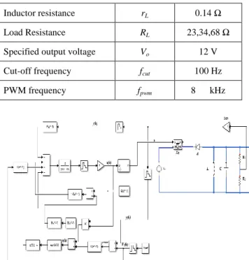
IMULATIONIn the first work [3], the dc-dc converter’s (which implements PWM with conventional SM Voltage Controller’s) are considered. Here in this work the DSM controller is introduced to improve the control procedure. The procedure of control is shown in Figure 3. Simulation was fulfilled on a B/B converter with the parameter values given in Table 1.
In order to test the robust feedback control strategy of the DSM with respect to the external perturbation and plant’s parameter deviation, a scenario of different values of input voltages (8 V, 12 V, 16 V), output resistance (23Ω, 34Ω, 68Ω)is taken to ensure the effectiveness of the system using QSM. The simulation is completed depending on the calculated values of the following parameters: sampling-time , switching gain , sensor’s gain , referent voltage, respectively.
Table 1.
The components of the buck-bust converter
Description Parameter Value
Input voltage Vi 8 V, 12 V, 16 V Capacitance C 1470 F Capacitor resistance rc 0.001 Ω Inductance L 300 H T 0 1 , a 1 1 (1 xT) , x= , k= o L V a e R C LC 2 xT a e 1 T ms 10 0.1
Inductor resistance rL 0.14 Ω
Load Resistance RL 23,34,68 Ω
Specified output voltage Vo 12 V
Cut-off frequency fcut 100 Hz
PWM frequency fpwm 8 kHz
Figure 3. The DSMC used in BB converter.
The schematic diagrams of the digital sliding mode controller method in Figure 3 are used in the simulation. With the input voltage, load resistance Vi 12 , V RL 34, the calculated parameters obtained by MATLAB/ SIMULINK, are: 2 1 1 1 ( ) 1 1.98 0.98 A z z z 1 1 ( ) 1.351 1.342 B z z 2 1 1 1 ( ) 1 1.067 0.2846 C z z z 0 1 , 0 0.9123 , 1 0.6956 e f f Roots: 0.9934 , 0.5335 , 0.5335
The final result of dc-dc BB converter using the digital sliding mode at input voltage 12 V, RL
= 34Ω can be illustrated in the following figures: Figure 4 demonstrates the resulting voltage of the B/B converter using digital sliding mode controller; this voltage is equal to 12 V after 0.5 sec with a small ripple.
Figure 4. The resulting voltage of buck/boost converter.
Figure 5. The error voltage of buck/boost converter.
The sensed voltage Vo at the output of the
converter is compared with the referent voltage, as a result of an error signal as in Figure 5. According to this figure the error signal approximately reach zero after 0.5 sec.
It is clear from Figure 6 that the system will move monotonically towards the switching plane, so the sliding mode maintains a zig-zag motion in the vicinity of the switching plane.
Figure 6. The switching function of buck/boost converter.
The input voltage and load resistance variation scenario are obtained in the following figures:
1. For Input voltage 8 V, load resistance RL =
34Ω, and calculated parameters by SIMULINK:
2 1 1 1 ( ) 1 1.9802 0.9802 A z z z 1 1 ( ) 1.3515 1.3425 B z z 2 1 1 1 ( ) 1 1.067 0.2846 C z z z 0 1 , 0 0.9132 , 1 0.6956 e f f Roots: 0.9934 , 0.5335 , 0.5335
Figure 7 illustrates the steady-state waveforms of the resulting voltage, error signal, and switching function.
Figure 7. The resulting voltage, error signal, switching signal of the buck/boost converter.
2. For Input voltage 12 V, load resistance RL =
34Ω, and calculated parameters by SIMULINK:
2 1 1 1 ( ) 1 1.9802 0.9802 A z z z 1 1 ( ) 1.3515 1.3425 B z z 2 1 1 1 ( ) 1 1.067 0.2846 C z z z 0 1 , 0 0.9123 , 1 0.6956 e f f Roots: 0.9934 , 0.5335 , 0.5335
Figure 8 illustrates the steady-state waveforms of output voltage, error signal, and switching function.
Figure 8. The resulting voltage, error signal, switching signal of the buck/boost converter.
3. For Input voltage 16 V, load resistance RL =
34Ω, and calculated parameters by SIMULINK:
2 1 1 1 ( ) 1 1.9802 0.9802 A z z z 1 1 ( ) 1.3515 1.3425 B z z 2 1 1 1 ( ) 1 1.067 0.2846 C z z z 0 1 , 0 0.9123 , 1 0.6956 e f f Roots: 0.9934 , 0.5335 , 0.5335
Figure 9 shows the steady-state waveforms of the resulting voltage, error signal, and switching function.
Figure 9. The resulting voltage, error signal, switching signal of the buck/boost converter.
4. For Input voltage from 12 V, load resistance RL = 23Ω, and calculated parameters by
SIMULINK: 2 1 1 1 ( ) 1 1.9709 0.9709 A z z z 1 1 ( ) 1.3472 1.3342 B z z 2 1 1 1 ( ) 1 1.067 0.2846 C z z z 0 1 , 0 0.9039 , 1 0.6862 e f f Roots: 0.9902 , 0.5335 , 0.5335
Figure 10 illustrates the steady-state waveforms of the output voltage, error signal, and switching function.
Figure 10. The resulting voltage, error signal, switching signal of the buck/boost converter.
5. For Input voltage 12 V, load resistance RL =
34Ω, and calculated parameters by SIMULINK:
2 1 1 1 ( ) 1 1.9802 0.9802 A z z z 1 1 ( ) 1.3515 1.3425 B z z 2 1 1 1 ( ) 1 1.067 0.2846 C z z z 0 1 , 0 0.9132 , 1 0.6956 e f f Roots: 0.9934 , 0.5335 , 0.5335
Figure 11 illustrates the steady-state waveforms of the resulting voltage, error signal, and switching function.
Figure 11. The resulting voltage, error signal, switching signal of the B/B converter.
6. For Input 12 V, load resistance RL = 68Ω,
and calculated parameters by SIMULINK:
2 1 1 1 ( ) 1 1.9847 0.9847 A z z z 1 1 ( ) 1.3536 1.3466 B z z 2 1 1 1 ( ) 1 1.067 0.2846 C z z z 0 1 , 0 0.9177 , 1 0.7 e f f Roots: 0.9949 , 0.5335 , 0.5335
Figure 12 illustrates the steady-state waveforms of the output voltage, error signal, switching function.
Figure 12. The output voltage, error signal, switching signal of the BB converter.
At the end the voltages adopted by simulation is filtered so as to avoid the low amplitude high frequency perturbances that can have a harmful effect on the control procedure.
V.
C
ONCLUSIONThis research study highlights the development of a digital-sliding mode controller that improves the performance of a non-linear converter, its modeling, design, and simulation. It has been proven that the output voltage of a closed circuit follows the equation obtained by the model
(yields a positive result). The proposed control strategy shows a significant stability that is consistent with the theoretical calculations. Finally, a practical solution for the nonlinearity of the voltage fluctuation is established using digital-sliding mode.