Paper
Industrial standardization and quantification of the carrier
concentration in semiconductor devices using electric SPM
Takaya Fujita,1* Akiya Karen,1,2 Hiroshi Ito3 and Daisuke Fujita4
1
Surface Analysis Laboratories, Toray Research Center Inc. (TRC), 3-3-7 Sonoyama, Otsu, Shiga 520- 8567, Japan
2
Global Research Center for Environment and Energy based on Nanomaterials Science (GREEN), National Institute for Materials Science (NIMS), 1-1 Namiki, Tsukuba, Ibaraki 305-0044, Japan
3
Research Institute of Instrumentation Frontier, National Institute of Advanced Industrial Science and Technology (AIST), 1-1-1 Umezono, Tsukuba, Ibaraki 305-8568, Japan
4
Advanced Key Technologies Division, National Institute for Materials Science (NIMS), 1-2-1 Sengen, Tsukuba, Ibaraki 305-8568, Japan
(Received: October 11, 2012; Accepted: November 10, 2012)
Scanning capacitance microscopy (SCM) is one of techniques imaging two-dimensional carrier distribu-tion in semiconductor devices. We have demonstrated that quantitative analysis of carrier concentradistribu-tion can be performed using calibration curves, which are statistically prepared for respective materials like silicon, silicon carbide, etc. The procedure was circulated to research organizations in domestic round robin test, and this method was found to be available from the viewpoint of comparability among users for the indus-trial standardization. It was also applied to other microscopes, and their profiles of carrier concentration coincide with each other, suggesting compatible to next-generation microscopes which would come up in the future.
1. Historical overview of SPM development and standardization
Scanning probe microscopy (SPM) is a collective term and consists of a family of microscopes and related tech-niques using a probe with a sharp tip that can image a three dimensional surface topography and analyze a sur-face property of specimens. Historically, it originated in the innovation of scanning tunneling microscopy (STM) in 1981 by Gerd Binnig and Heinrich Rohrer at IBM Zurich Research Laboratory [1], enabling us to research surface physics and chemistry with atomically resolution. Succeeding STM, the next most important developments was atomic force microscopy (AFM) applicable to either insulator or conductor [2]. Our company Toray Research Center Inc. has started a business of research and analy-sis service using AFM (ultra-high vacuum AFM system made by Electrotechnical laboratory, AIST) since 1989.
In the 1990’s, a variety of the SPM techniques was developed and the first commercially launched from
Digital Instruments Inc. (emerged with Bruker AXS, then followed by Veeco instruments). Using this commercial AFM, we reported the first study of an evaluation of ox-ygen-ion scattered craters with ripping structure affecting the yields of secondary ion on a Gallium Arsenide (GaAs) surface [3]. Around the 2000 year, the SPM market was grown and increasing. The operation modes were designed for direct observation and manipulation of biological molecules, mechanical evaluation of polymers, characterization of magnetic materials in data storage, electric testing and failure analysis of semiconductor devices, etc. Over the thirty years, we have learned the applications had changed from fundamental science in vacuum to practical analysis in air or fluid. Nowadays, SPM has been used as not only general purpose tools in laboratories but also inspection tools equipped with au-tomation system in which robots load or unload the probes and samples in industrial fabrication.
standardization in the top-down approach, without an exception of SPM, as it progressively enters the mature phase. According to technical roadmap of SPM stan-dardization, the global pre-standardization research was initiated by committee TWA29 of Versailles Project on Advanced Materials and Standards (VAMAS) in 2002. As for international organization for standardization (ISO), TC201 (surface chemical analysis) established the sub committee SC9 for SPM in 2004. In Japan, our stan-dardization activities concerning SPM (JSCA, SPM-WG) have contributed to a publication of Interna-tional Standard ISO 28600 on standard data transfer format for SPM in 2011 [4], drafts of IS (DIS), new work item proposals (NWIP) and technical reports (TR) for related and further advanced probe technologies.
2. Scope of carrier concentration profiling in semi-conductor devices using electric SPM
In semiconductor application, one of the most impor-tant matters is evaluation of carrier concentration distri-bution in real devices like a metal-oxide-semiconductor field-effect transistor (MOSFET), where both high de-tection sensitivity and spatial resolution are needed. Scanning capacitance microscopy (SCM) and scanning spreading resistance microscopy (SSRM) were based on contact mode AFM techniques imaging electric proper-ties in semiconductor devices, such as the free carrier distribution [5]. These two microscopes had been ex-pected as the above-mentioned analytical solution in the earlier 2000’s, but no more they could be applicable to the latest scaling down MOSFET in large scale integra-tion (LSI). During these ten years, in our great deal of practical experiences of analysis service, we concluded that SCM has been suitable for the carrier concentration estimation and SSRM for high resolution imaging, in a mutually complementary manner. Actually, SCM is widely used at users’ sites and has enough reproducibil-ity of the signal corresponding to the carrier concentra-tion.
3. Procedure of statistical estimation of carrier con-centration from SCM signal
A UHF capacitance sensor from RCA technology of the 1970’s, which is equipped with SCM, can detect a small movement of elementary charges of less than 10-19F, though the sensor cannot count the number of the
charges. Therefore, the characteristic of sensor can be easily changed by the condition of the surface and probe, making it difficult to control output signals. In princi-ple, SCM using this sensor can feel amplitude modula-tion (AM) or frequency modulamodula-tion (FM) shift of a reso-nance oscillation of the transmitted Giga Hertz-band wave, mixed with a small ac voltage of dV (about 100 kHz) applied to the semiconductor sample. When a metal coated conductive probe touched on the surface, a local MOS capacitor is formed beneath the thin oxide, as shown in figure 1. In this area, an accumulation and de-pletion of the volume change induced by the dV can be detected as a signal corresponding to the capacitance change of dC through lock-in-amplifier. The interpreta-tion of the SCM’s resonance shift signal, which has been called as ‘dC/dV’, qualitatively follows a conventional method measuring high frequency capacitance verses voltage (C-V) relationship, though the sensor does not directly detect the capacitance but the change of the fre-quency, that is a reason of the lack of repeatability.
Fig. 1 Schematic of SCM. AC bias voltage oscillates a local MOS capacitor beneath the probe
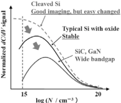
Fig. 2 Correlation between carrier concentration and normal-ized dC/dV signals.
In such a background, we tried to examine and found a kind of correlations between concentration and dC/dV
signals as shown in figure 2, since there were no trace-able ways except for using amount of well-known sam-ples like dopant implanted wafers, as well as real devices. At last, the tendency of the sensor’s characteristic has been resulted from thousands of data which contribute to decreasing errors. In our method, not absolute values of the signal but a sequence of functions is necessary for the estimation, in which logarithm values of carrier concen-tration N in the horizontal axis were calculated from dC/dV signals in the vertical axis. Figure 3 shows an initiation procedure of plotting data and drawing the cal-ibration curve in the case of the reference sample of sili-con carbide (4H-SiC) epitaxial wafers. The vertical axis of the dC/dV signal was normalized the maximum to 1. By calculating inversely, in-plane distribution of the concentration with less than 20 % was also revealed in the profile of figure 4.
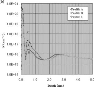
Figure 5 shows one of the results of practical analysis of real devices. Each implanted diffusion layers were observed in the dC/dV image on the cross-section of a power MOSFET [6]. In depth profiles of figure 5 (b), it is possible to quantitatively compare with the peak val-ues. Similarly, this method has been applied to other ma-terials like indium phosphate (InP) laser diodes for opti-cal communication, copper indium gallium selenide (CIGS) thin layers for photovoltaic cell and etc.
Fig. 3 Calibration curve for 4H-SiC sample plotted by using carrier concentration of epitaxial wafers.
Fig. 4 Distribution of the carrier concentration in the 4H-SiC epitaxial wafer. (a) dC/dV image of the surface and (b) a lateral profile of the carrier concentration along the white line in Fig. 4(a).
Fig. 5 SCM observation of a power MOSFET. (a) dC/dV image of the cross-section and (b) depth profiles of the statisti-cally estimated carrier concentration.
4. Round robin test of estimation method for carrier concentration using SCM, SNDM, etc
The increasing popularity of SPM has given some kinds of effects for driving needs in a daily use and pro-posing industrial standardization of available techniques, that is the bottom-up approach in contrast of metrology standardization. In this case, round robin test is a pre-ferred way to circulate the samples or recipes of the measurements among laboratories in the world wide for a short period, since it is possible to collect data for the proofs of standardization instead of traceable way.
User-to-user compatibility with SCM data was exam-ined in domestic prior to global circulating. We used IMEC's epitaxial wafers with stair-structure profile which were widely used for the reference sample of do-pant and carrier concentration for conventional spreading resistance measurement techniques [7]. They made pile-up structures in the boundaries as buffer layers for avoiding dopant diffusion. We also prepared AIST's do-pant implanted wafers with continuous dynamic range for the carrier concentration evaluation, of which depth structure is similar to practical devices for both dopant and carrier concentration evaluation. Figure 6 shows results of the IMEC’s sample. Apparent difference in images was observed, but the carrier profiles calculated independently using the users’ calibration curves were almost coincident each other except for a couple of missed structures. Since participants of the round robin test do not have enough times for statistical estimations, the discrepancy of the carrier concentration is not
ignor-able as now but the accuracy would be improved by re-vising their calibration curve steadily.
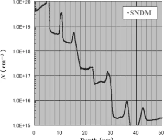
Electric SPM techniques would progress year by year, while the computing technology was updated together. It may be time to think we discuss the substitution of next generation microscopies for SCM. In our previous study, it has been demonstrated that both profiles with the concentration estimated from different signals such as the dC/dV of SCM and spreading resistance R of SSRM were coincident under the same condition of the sample [8]. Finally, we introduce a state-of-the-art scan-ning nonlinear dielectric microscopy providing with pos-sibility of atomic resolution [9], which is one of the most likely substituting technologies. Figure 7 shows a depth profile of the IMEC’s sample obtained by a commercial SNDM launched by SII Nanotechnology Inc. The carrier concentration was calculated by the same way as SCM, and good fitting with each other was also confirmed.
Fig. 6 Round robin test for user-to-user compatibility with SCM data of IMEC's epitaxial wafer. (a) dC/dV images and (b) depth profiles at users’ sites
Fig. 7 Depth profile of the statistically estimated carrier con-centration from SNDM data of IMEC's epitaxial wafer.
5. Conclusions and future plans
Statistical method using calibration curve is found to be effective for quantitative analysis of carrier concentra-tion in semiconductor devices. It is also suggested that estimated concentration are comparable among users. This method does not depend on measurement mode, suggesting compatible to SCM, SSRM, SNDM and other next generation electric SPM.
Needs of the quantification of carrier concentration using electric SPMs are still strong in the semiconductor industry, and this kind of industrial standardization would be important and hurried as long as it is available, even if there are no proofs for traceable guarantees of the quantification. Because we know users need analytical solutions in the very front of them. This is also because they cannot wait the time until calibration certificated. In this way, relative values such as carrier concentration obtained by electric SPMs should be standardized under each country agreement. Then, we prepare a document for the analytical protocol of the carrier concentration conversion procedure in our working group of ISO/TC201/SC9. We also plan to circulate it in the over-seas research organization in VAMAS’s round robin test program for the timely industrial standardization. 6. Acknowledgement
This work was partially supported by Ministry of Economy, Trade and Industry (METI). We thank Dr. Gonda of AIST for tutorial discussions about the differ-ence between metrological and industrial standardiza-tion.
7. References
[1] G. Binnig and H. Rohrer, Helv. Phys. Acta 55, 726 (1982).
[2] G. Binnig, C.F. Quate and Ch.Gerber, Phys. Rev. Lett. 56, 930 (1986).
[3] A. Karen, K. Okuno, F. Soeda and A. Ishitani, J. Vac. Sci. & Tech. A 9, 2247 (1991).
[4] ISO 28600: 2011, Surface chemical analysis --Data transfer format for scanning-probe microscopy-. [5] P. De Wolf, W. Vandervorst, H. Smith and N. Khalil,
J. Vac. Sci. Technol. B 18, 540 (2000). [6] T. Fujita, J. Vac. Soc. Jpn. 54, 445 (2011).
[7] T. Claryssed, M. Caymax, P. De Wolf, T. Trenker and W. Vandervorst, J. Vac. Sci. Technol. B 16, 394 (1998).
[8] T. Fujita, The 3rd Internattional Symposium on SPM Standardization, extended abstract, 45 (2012). [9] K. Ohara and Y. Cho, Nanotechnology 16, 54 (2005).
![Figure 5 shows one of the results of practical analysis of real devices. Each implanted diffusion layers were observed in the dC/dV image on the cross-section of a power MOSFET [6]](https://thumb-ap.123doks.com/thumbv2/123deta/8397728.1302880/3.892.462.759.129.617/figure-results-practical-analysis-devices-implanted-diffusion-observed.webp)