JAIST Repository: Study on Integrated Ferroelectric Gate Field-Effect Transistor Memory with an Intermediate Electrode
5
0
0
全文
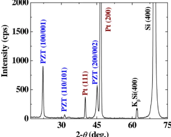
(2) Study on Integrated Ferroelectric Gate Field-Effect Transistor Memory with an Intermediate Electrode Laboratory of Semiconductor Materials Bui Nguyen Quoc Trinh Student Number: 440209 Introduction Ferroelectric gate field-effect transistors (FeFETs) are well known as field-effect transistor (FET) type memory, in which the gate insulator is a ferroelectric material. This FeFET memory has attracted much attention because it has prominent advantages such as nonvolatile, nondestructive readout, low writing voltage, fast writing speed, high endurance and high packing density. However, it is very difficult to fabricate an FeFET with perfect memory ability. If a ferroelectric film is directly deposited on a Si substrate, the constituent atoms from the deposited ferroelectric film, such as Pb and Bi, easily diffuse into the Si substrate, and thus, the interfacial electrical properties become very poor. Generally, a buffer layer with a high dielectric constant is inserted between the ferroelectric film and Si substrate, forming a metal–ferroelectric–insulator–semiconductor structure (MFIS). Many researchers reported that, using this MFIS structure, the retention time has a tendency to be very short because the generation of leakage current to/from the Si and a reduction in the remnant polarization are caused by the essentially preserved charge on the insulator layer. Furthermore, a high writing voltage is needed because of the voltage drop at the insulator and transistor layers. In order to solve these issues of the conventional FeFET memories, a FeFET memory with an intermediate electrode for data writing (called as IFFET) was investigated. With the intermediate electrode of IF-FET memory, a writing voltage is lowered because it is applied only to the ferroelectric capacitor, and a long retention time is expected by keeping the remnant polarization state under zero bias condition without preserving charge on the gate of MOSFET. The main goal of this study is to fabricate a well-operative IF-FET memory integrated on Si substrate, and to find new writing and reading methods for improvement in the nondestructive readout of IF-FET.. Operational Principle of IF-FET Memory Figure 1 shows the schematic basic circuit of IF-FET memory which consists of a ferroelectric capacitor Cf connected serially to an n-channel reading MOSFET transistor (R-FET). For data-writing, we apply a writing pulse voltage VW only to the Cf directly using the intermediate electrode. Then, the polarization state of the Cf is. Cfl, Small. 2. Polarization (µC/cm ). 40. VW. W-FET. Cf. VR VI. C0. R-FET. S D. ID. Intermediate electrode. 20 0. -20. 100 kΩ V0. Pr. +. Cfh, Large. Pr-. VD0 = 2 V. Fig. 1: Schematic basic circuit of IF-FET memory for investigating the memory operation.. -40 -300 -200 -100 0 100 200 Electric Field (kV/cm). 300. Fig. 2: A typical polarization-electric field (P-E) hysteresis loop of the ferroelectric capacitor with 200nm-thick poly-PZT film.. 1.
(3) set positive (Pr+) for VW > 0 or negative (Pr-) for VW < 0. Although the W-FET for data-writing is connected to the R-FET, we did not use it in this study. For data-reading, a positive reading voltage VR is applied between the top electrode and the source of R-FET. Because the Cf for Pr+ (Cfl) is much smaller than that for Pr- (Cfh) when VR > 0 (see Fig. 2), the drain current ID for the Pr- state is larger than that for the Pr+ state owning to intermediate voltage VI = CfVR/(Cf + C0), where C0 is the input capacitor of the MOSFET. Thus, by detecting the ID the memory state can be read.. Experimental Method. KβSi(400). Pt (200). PZT (110/101). Pt (111) PZT (200/002). PZT (100/001). Intensity (cps). Fig. 3: XRD patterns of the normal PZT film deposited on (a) the highly (100)-oriented Pt films on the RuOx/SiO2/Si substrate.. Results and Discussion. 0. 10 2. Current density (A/cm ). It was found that the preferential orientation of Pt films deposited on the RuOx/SiO2/Si substrates depends on the sputtering power, pressure and deposition time. The preferential orientation of the Pt film can be explained by considering surface energy and strain energy in the Pt film. If the contribution of surface energy to the difference in overall energy is predominant, the preferential orientation tends toward Pt(111), but if that of strain energy is predominant, the preferential orientation tends toward Pt(100). In fact, the highly (100)oriented Pt films were successfully prepared, as seen from the high (200) Pt peak in Fig. 3. As a result, the (100/001)-oriented PZT film was successfully grown on the highly (100)-oriented Pt film on RuOx/SiO2/Si substrate by sputtering as shown in Fig. 3. Also, PtOx/RuOx double layer as a top electrode was used in order to reduce leakage current. By using the PtOx/RuOx. Si (400). For fabrication of the IF-FET memory, a 6-nm-thick SiO2 was used as a buffer layer at the gate of MOSFET because the interface between SiO2 and Si is the most ideal. Then, on the SiO2, a double-layer structure consisting of a 700-nm-thick Pt film and a 60-nm-thick RuOx film was formed as the bottom electrode by sputtering, in order to suppress the fatigue properties of the memory because oxygen in RuOx can supply to the PZT film. Since SiO2 is amorphous without crystallographic information, 200-nm-thick Pb(Zr0.52Ti0.48)O3 (poly-PZT) films prepared by sputtering as ferroelectric layers of the IF-FET memory were polycrystalline, which is favorable for industry aspect because of the easy and low cost technique of mass production. Actually, for PZT film 2000 deposition, a thin PZT seed layer was deposited at 600oC for a short time of 2 min, followed by an amorphous PZT layer 1500 deposited at 300oC for 28 min, and then it was crystallized at around 600oC for 15 min in air. 1000 To evaluate nondestructive characteristics, after only one data writing, the memory state was readout 10 times with an 500 interval of 1 min after each readout. During retention, the top electrode was grounded together with the source and drain of the 0 R-FET transistor, the intermediate electrode was floated, and the 30 45 60 75 2-θ (deg.) gate of W-FET is grounded.. -2. 10. -4. 10. -6. 10. -8. 10. -10. 10. -4. -2. 0 2 Voltage (V). 4. Fig. 4: I-V characteristics of the A-PZT film crystallized at 600oC after the RuOx/PtOx double top electrodes annealed at 450oC.. 2.
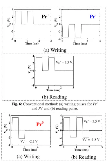
(4) VR (V). VW (V). VR (V). VW (V). VW (V). double top electrode the leakage current density is about 10-6 A/cm2 at ± 4 V as shown in Fig. 4, whereas it is about 10-5 A/cm2 by using the RuOx single top electrode. Figure 5 shows the photograph of the integrated IF-FET memory cell fabricated on a p-type Si substrate (a) and the schematic drawing of one cell (b). Threshold voltage of the R-FET is determined to be about 1.2 V. For conventional data-writing, two positive and R-FET negative square pulses of 3.5 V induced the Pr+ and the C Gate Pr- memory states as shown in Fig. 6 (a), respectively. For conventional data-reading, a unipolar square pulse Drain Source train of 3.5 V was applied as shown in Fig. 6 (b). Ideally, the readout operation of IF-FET memory Gate W-FET 200µm Source should be nondestructive as an ultimate FeFET (b) (a) memory. However, actually, it was found that the IFFig. 5: (a) Photograph and (b) schematic drawing of the FET memory showed destructive readout, especially integrated IF-FET memory cell. F-FET consists of a for the Pr memory state. In fact, although the initial ferroelectric capacitor Cf connected serially to an n-channel MOSFET (R-FET). W-FET is used as a switch for data difference in output voltage between Pr+ and Pr-, ∆V0 writing, and C has the same structure with the Cf for was 0.98 V, the differences decreased with number of checking ferroelectric properties. reading. This poor nondestructive readout for the Pr4 4 was resulted from large amount of nonreturned domain + 2 2 from negatively polarized domains. Pr PrTherefore, we proposed new data writing and 0 0 reading methods. For the new data-writing, we used -2 -2 the Pr+ state and the Pr0 state instead of the Pr- state. -4 -4 0 1 2 3 0 1 2 3 The new Pr0 was used to reduce the amount of Time (ms) Time (ms) negatively polarized domains in data writing. The Pr0 (a) Writing 4 was induced by a combined pulse with a positive VR+ = 3.5 V voltage (VW+) and a negative voltage (VW-). The degree 2 of polarization can be controlled by adjusting the VW-. 0 For the new data-reading, a negative voltage VR was -2 applied, following a positive voltage VR+ in order to -4 0 1 2 3 reduce amount of nonreturned domains. By increasing Time (ms) the VR-, the switched positive domains due to VR+ can (b) Reading be reswitched to the initial states, and the memory state Fig. 6: Conventional method: (a) writing pulses for Pr+ and Pr- and (b) reading pulse. can be recovered after each reading, which means that 4 4 the nondestructive readout can be improved. However, + VR+ = 3.5 V because the small VW makes the ∆V0 between Pr and 0 2 2 Pr Pr0 reduce and the large VR- makes the nondestructive 0 0 readout for the Pr+ degrade, we optimized the -2 -2 VR- = -1.8 V Vw- = -2.2 V amplitude of VW- and VR-. -4 -4 0 1 2 3 0 1 2 3 The VW+ was determined from the polarizationTime (ms) Time (ms) voltage P-V hysteresis loop of the Cf, at which the (a) Writing (b) Reading saturation of polarization begins. The VW- was adjusted Fig. 7: New method: (a) writing pulse for Pr0 instead of Pr- and around -VW+/2 from viewpoints of output voltage and (b) reading pulse.. 3.
(5) st. 1 reading nd 2 reading th 10 reading. 1. 0. 0. 1. Pr+ 2. Time (ms). 1. 0. 3. st. Pr0. 1. 1 reading nd 2 reading th 10 reading 2 3. Time (ms). (a) Conventional 2. 2. 1. st. 1 reading nd 2 reading th 10 reading. V0- (V). Conclusions. 2. V0- (V). V0+ (V). 2. V0+ (V). nondestructive characteristics. The VR+ was determined from analyzing the memory operation, and the VR- was optimized from a viewpoint of the nondestructive characteristics. The actual values are shown in Fig. 7. As a result, when the Pr0 was induced by a combined pulse with VW+ = 3.5 V and VW- = -2.2 V, and a new reading voltage with VR+ = 3.5 V and VR- = -1.8 V was applied, the nondestructive readout characteristics were further improved although the ∆V0 was reduced by 21%, compared with the conventional method.. 1. st. 1 reading nd 2 reading th 10 reading 1 2. A highly (100)-oriented Pt film prepared by Pr0 Pr+ sputtering plays a role as a seed layer so that a mainly 0 0 0 3 0 1 2 3 (100/001)-oriented PZT film was successfully grown Time (ms) Time (ms) on it. (b) New An integrated IF-FET was successfully Fig. 8: Nondestructive readout characteristics: (a) previous fabricated on Si wafer. The nondestructive readout writing and reading method and (b) new method. characteristics of the integrated IF-FET were obtained by using the new writing and reading methods. Therefore, it is expected that the new method will promote commercialization of IF-FET in future as a proper substitute for conventional FeFET.. Table of Contents Chapter 1 Chapter 2 Chapter 3 Chapter 4 Chapter 5 Chapter 6 Chapter 7. Introduction………………………………………………………………………………. 1 Experimental Procedures and Film Characterization…………………………………..... 22 Control of Preferred Orientation of Pt Film …………………………………………… ..44 Crystalline and Electric Properties of PZT Film………………………………………… 57 Discrete Circuit of IF-FET Memory…………………………………………………….. 71 Fabrication of Integrated IF-FET Memory……………………………………………… 92 Conclusions and Future Work ………………………………………………………….. 105. List of Publications 1. Bui Nguyen Quoc Trinh and Susumu Horita, Operation of Ferroelectric Gate Field-Effect Transistor Memory with Intermediate Electrode using Polycrystalline Capacitor and Metal–Oxide–Semiconductor FieldEffect Transistor, Japanese Journal of Applied Physics, Vol. 45, 7341–7344 (2006). 2. Bui Nguyen Quoc Trinh and Susumu Horita, Control of Preferential Orientation of Platinum Films on RuO2/SiO2/Si Substrates by Sputtering, Japanese Journal of Applied Physics, Vol. 45, 8810-8816 (2006).. 4.
(6)
図

関連したドキュメント
We prove the coincidence of the two definitions of the integrated density of states (IDS) for Schr¨ odinger operators with strongly singular magnetic fields and scalar potentials:
In fact in order to show that Condorcet rankings are medians we are going to use a more general notion of median namely the notion of metric median in a metric space.. I begin by
In the further part, using the generalized Dirac matrices we have demonstrated how we can, from the roots of the d’Alembertian operator, generate a class of relativistic
On figures 2 and 6, the minimum, maximum and two of the intermediate free energies discussed in subsections 3.5 and 6.5 are shown for sinusoidal and exponential histories with n =
In Section 6 various semigroups associated with above mentioned unitary processes are studied and using them a Hilbert space, called noise space and structure maps are constructed
We start by collecting, in Section 1, a number of notions and results about Real groupoids most of which are adapted from many sources in the litera- ture [15, 19, 25]; specifically,
(4S) Package ID Vendor ID and packing list number (K) Transit ID Customer's purchase order number (P) Customer Prod ID Customer Part Number. (1P)
If DISB# and VCC are ready, but the voltage across the boot capacitor voltage is lower than 3.1 V, NCV303150 ignores the PWM input signal and starts the boot refresh circuit.. The
