PLOYBUSSARA GOMASANG
Student ID: NB17508
Major: Functional Control Systems
Supervisor
Prof. Dr. Kazuyoshi Ueno
A thesis submitted in fulfilment of
the requirements for the award of the degree of
Doctor of Philosophy
CANDIDATE’S DECLARATION
It is hereby declared that this thesis or any part of it has not been submitted
elsewhere for the award of any degree or diploma.
Signed: ____________________
(Ploybussara Gomasang)
Student No.: NB17508
Certified by: ____________________
Dedicated
To
Undertaking a Ph.D. at Shibaura Institute of Technology (SIT), Japan, has been a truly life-changing experience for me and here I sincerely thank many people without their support and guidance this work would not archived smoothly.
Above all, I would like to express the deepest appreciation to my supervisor, Prof. Dr. Kazuyoshi Ueno, Department of Electronic Engineering (SIT), Japan, for all the support and advice that he provided me during this period, while I have taken this research at SIT and also the time I spent in Japan. Without his guidance and constant feedback, this Ph.D. would not have been achievable.
Also, I would like to express my deepest gratitude to Prof. Shinji Yokogawa (The University of Electro-Communications, UEC), Prof. Hiroki Ago and his group (Kyushu University), Prof. Susumu Okada and his group (University of Tsukuba), and Dr. Nataliya Nabatova-Gabain and Ms. Yoko Wasai (Horiba Techno Service) for their collaborations and fruitful discussions on some topics related to my research.
I am grateful to Prof. Hiroyasu Ishikawa (SIT), Prof. Tadashi Maeda (SIT), Prof. Kentaro Kyuno (SIT), Prof. Eiichi Kondoh (University of Yamanashi), and Prof. Shinji Yokogawa (UEC) for their kind review of my dissertation.
Also, I would like to express my gratitude to Assoc. Prof. Dr. Rardchawadee Silapunt (King Mongkut's University of Technology Thonburi) for being such an inspiration and all the support throughout my education.
I gratefully acknowledge the funding which I received towards my doctoral course at SIT from the Hybridge Twinning program (SIT, for the 1st year), the Ministry of Education, Culture, Sports,
Science and Technology (MEXT) scholarship from Japanese government, Core Research for Evolutional Science and Technology (CREST) Grant Number JPMJCR1532 from the Japan Science and Technology Agency (JST), and SIT Research Center for Green Innovation.
I am thankful to Mrs. Mikiko Nikami, all members of Nanoelectronic Laboratory (SIT), all friends, and all concerned for their help during my studying.
Special thanks to my parents, my beloved Tony, and the lovely Kalour group for continuous encouragement provided to me.
Semiconductor memory (SM) devices, which can be used as storage media in various applications, have been extensively developed. Because of the rapid increase of digital recording in the world, SM devices are also expected to use for long-term storage of valuable digital data over 100 years. Regarding advanced SM technologies, copper (Cu) has been widely used as interconnect and bond pad material in place of Al to enhance the electrical conductivity and current endurance. Therefore, the long-term reliability of Cu used in SMs is a serious concern for the long-term storage application (>100 years). A potential cause for the failure of long-term data storage is Cu oxidation due to moisture. To avoid Cu oxidation, an impermeable thin film coat can be used. Nanocarbon materials, such as graphene and amorphous carbon (a-C) composites, are excellent candidates due to their small atomic radius of carbon. In the beginning, high-quality large-grained graphene was studied its potential and issues in preventing the Cu surface from oxidation in principle because its forming temperature is still high and not compatible with the current LSIs fabrication. Then, the properties of room-temperature nitrogen-doped a-C (a-C:N) were investigated and expected as a practical method to maintain the Cu surface from oxidation for more than 100 years. Before improving the long-term resistance of Cu against oxidation due to moisture, the effects of Cu oxidation on the sheet resistance were studied under accelerated conditions using a temperature humidity storage (THS) test. In addition, the dependency of Cu oxidation on the temperature and humidity was studied, then, the prediction model of Cu lifetime and its important parameters were derived. The Cu lifetime against humidity was estimated based on the proposed prediction model.
Large-grain single-layer graphene (SLG) was deposited by high-temperature chemical vapor deposition (CVD) for coating on the Cu surface. SLG was demonstrated the potential as an atomic-layer barrier against moisture. The THS test shows that large-grain SLG protects large areas of the Cu surface and only areas with grain boundaries and defects were oxidized.
issue. It can be used to cover the areas of SLG grain boundaries and prevent galvanic corrosion during the THS test. In addition, TLG can be used to protect the Cu surface, ensuring the efficiency of graphene in protecting the sample surface from oxidation due to moisture.
However, it is still difficult to apply graphene as moisture barrier of Cu metallization in current LSIs fabrication because of the high-temperature deposition of graphene. Therefore, a-C:N was studied as an alternative nanocarbon material that can be simply deposited by sputtering at room temperature. The THS test results show that a-C:N with an Ar:N2 ratio of 90:10 can preserve the
sheet resistance of an a-C:N/Cu sample for ~400 years (at 27℃/60% RH) based on the proposed prediction model. The XPS depth profiles obtained after the THS test confirm the excellent efficiency of a-C:N in preventing Cu oxidation due to moisture.
Page
Acknowledgements
I
Abstract
II
Contents
IV
List of Figures
VIII
List of Tables
XIII
List of Publications
XIV
Chapter
1. Introduction
1–21
1.1. Overview 1
1.2. History of digital data storage 2 1.3. Cu metallization used in SM devices: background and issues 4
1.4. Overall objective 6
1.5. Review of nanocarbon materials: fabrication and properties 7
1.5.1. Graphene 8
1.5.2. Amorphous carbon and nitrogen-doped amorphous carbon 9 1.6. Literature review related to the objective of this research 10 1.7. Aim and approach to reach the goal 14
1.8. Structure of the thesis 15
References 18
2. Film deposition, test, and methodology
22–38
2.1. Overview 22
2.2. Fabrication methods 22
2.2.1. Substrates cleaning 22
2.2.2.2. Cu sputtering on an Al2O3 substrate in preparation of graphene growth 24
2.2.3. Deposition and transfer of SLG 25 2.3. Temperature humidity storage test 26
2.4. Methodology 28
2.4.1. Raman spectroscopy 28
2.4.2. X-ray photoelectron spectroscopy 30
2.4.3. Spectroscopic ellipsometer 32
2.4.4. Optical microscopy 33
2.4.5. Scanning electron microscope 34 2.4.6. Transmission electron microscopy 35
2.4.7. Four-probe method 36
References 37
3. Copper surface oxidation and its effects on sheet resistance
39–60
3.1. Introduction 39
3.2. Experimental methods 39
3.3. Results and discussion 42
3.3.1. Results of experiment 1: 42
3.3.1.1. Normalized sheet resistance change depending on accelerated humidity 42 3.3.1.2. XPS analysis for the nonlinear dependence on the humidity 43 3.3.1.3. Mechanism for the nonlinear dependence of normalized sheet resistance change 46
3.3.2. Results of experiment 2: 48
3.3.2.1. Normalized sheet resistance depending on temperature and humidity 48 3.3.2.2. Difference of Cu-oxide thickness determined by XPS depth profiles 50 3.3.2.3. Mechanism for normalized sheet resistance saturation with longer THS time 53 3.3.2.4. Cu lifetime prediction model 55
3.4. Summary and conclusions 57
References 59
4.3. Results and discussion 68 4.3.1. Comparison between uniform SLG/Cu and bare Cu after THS test 68 4.3.2. Oxidized Cu thickness dependence on SLG quality in non-uniform SLG/Cu 74
4.4. Summary and conclusions 80
References 81
5. Stacked graphene layers to improve moisture barrier
83–98
5.1. Introduction 83
5.2. Experimental methods 84
5.3. Results and discussion 84
5.3.1. Analysis of Cu oxidation on SLG-coated Cu surface 84 5.3.2. Artificial stacking of CVD-SLG to cover the underneath grain boundaries 87 5.3.2.1. Change of surface color during THS test observed by OM 87 5.3.2.2. Evolution of Cu oxidation measured by XPS during THS test 89
5.4. Summary and conclusions 96
References 97
6. Nitrogen-doped amorphous carbon for practical moisture barrier
99–112
6.1. Introduction 99
6.2. Experimental methods 99
6.3. Results and discussion 100
6.3.1. Film characteristics measured by TEM and XPS 100 6.3.2. Efficiency verification of a-C:N against oxidation after THS test 101 6.3.2.1. Evolution of normalized sheet resistance measured by four-probe method 101 6.3.2.2. Change of surface color observed by OM 104 6.3.2.3. Change of surface morphology observed by SEM 105
6.3.2.4. XPS depth profiling 106
6.3.3. Mechanism of preventing Cu oxidation with a-C:N layer 108
6.4. Summary and conclusions 111
References 112
7.1. Overall conclusions 113 7.2. Conclusions for each chapter 113
7.2.1. Chapter 3 113
7.2.2. Chapter 4 114
7.2.3. Chapter 5 114
7.2.4. Chapter 6 115
Figure 1.1. Nonvolatile storage devices. 2
Figure 1.2. Schematic of a chip cross-section with copper interconnect 5 including the FEOL and BEOL layers.
Figure 1.3. (a) Schematic of an LSI package with wire bonding and 6 scanning electron micrographs showing (b) the top view and
(c) the cross section of gold wire bonded to the copper pads.
Figure 1.4. Structures of graphene and amorphous carbon. 8
Figure 1.5. Ternary phase diagram showing different amorphous carbon types. 10
Figure 1.6. Flowchart of the dissertation. 17
Figure 2.1. Schematic diagram of DC/RF magnetron sputtering system. 24
Figure 2.2. Schematic of the transfer of SLG onto SLG/Cu as BLG/Cu. 25
Figure 2.3. Temperature and humidity chamber. 27
Figure 2.4. Steps used to increase the temperature and humidity 27 to achieve the target conditions (85℃/85% RH).
Figure 2.5. Energy level diagram showing Rayleigh and Raman scattering 28 (Stokes and anti-Stokes lines)
Figure 2.6. Photoemission process in XPS. 31
Figure 2.7. General principle of ellipsometry. 32
Figure 2.8. Basic construction of OM. 33
Figure 2.11. Schematic diagram of a four-point probe. 36
Figure 3.1. Normalized sheet resistance of the first experiment 42 measured before and after 25, 50, and 100 h of THS test.
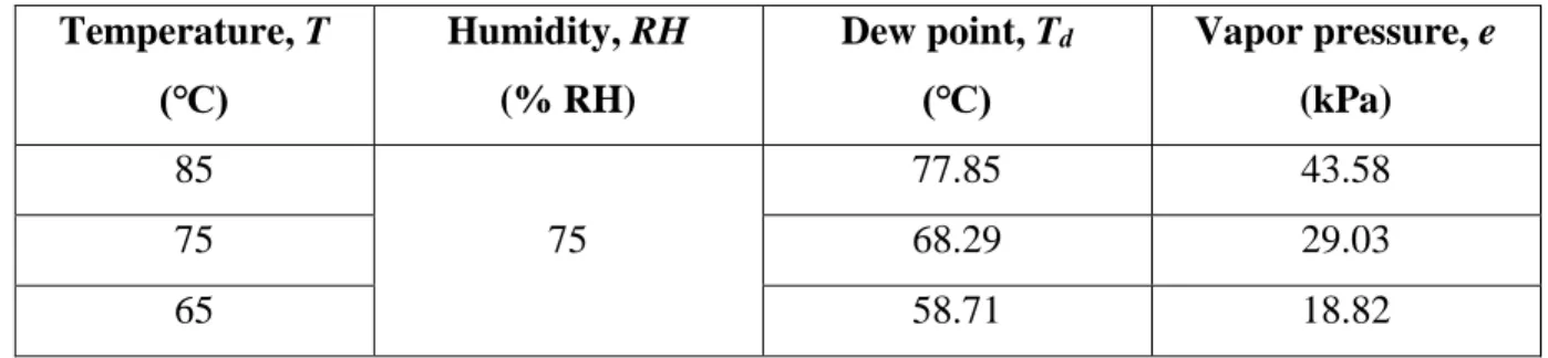
Figure 3.2. Comparison of normalized sheet resistance after 100 h of THS test, 43 indicating nonlinear dependence on the humidity.
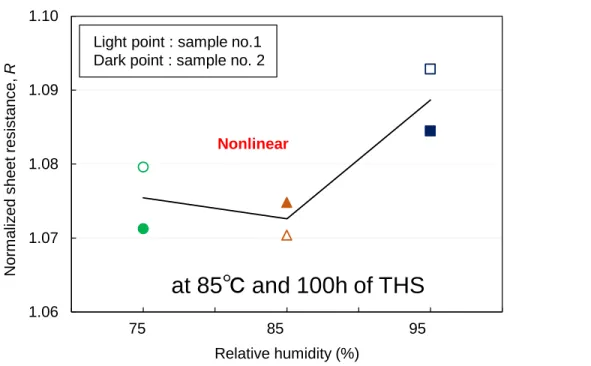
Figure 3.3. O/Cu atomic concentration ratios measured after 100 h of THS test, 44 indicating the O/Cu ratios linearly increase with humidity.
Figure 3.4. Cu 2p XPS spectra measured after 100 h of THS test under the conditions 45 (a) 75% RH, (b) 85% RH, and (c) 95% RH at 85°C.
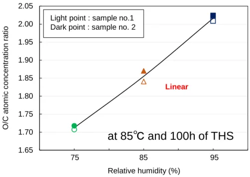
Figure 3.5. Proposed model to explain the difference of Cu-oxide structure 48 between 75 and 85% RH.
Figure 3.6. Time evolution of the normalized sheet resistance (R) during THS test 49
under the acceleration conditions of temperature and humidity dependence tests or vapor pressure (in kPa).
Figure 3.7. A previous report of parabolic rate constants (kp) showing in terms of 49 weight change per area per time (mg2cm-4h-1) during Cu-oxide formation with
water vapor pressure (pH2O, atm)
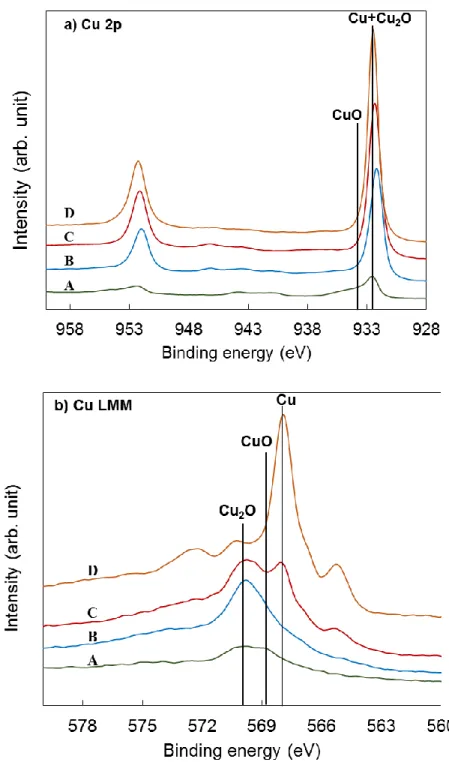
Figure 3.8. XPS depth profiles of (a) temperature and (b) humidity dependence tests. 51 Figure 3.9. Comparison of (a) Cu 2p and (b) Cu LMM spectra indicating 52
Cu2O+CuO of the top surface (“A”), dominant Cu2O after the first etching (“B”),
Cu2O+Cu at the interface (“C”), and Cu at the final etching (“D”), respectively.
Figure 3.10. Relative compositions of Cu(II) in CuO and Cu(I) in Cu2O estimated from 54
Cu-oxide thickness under various acceleration conditions of THS test.
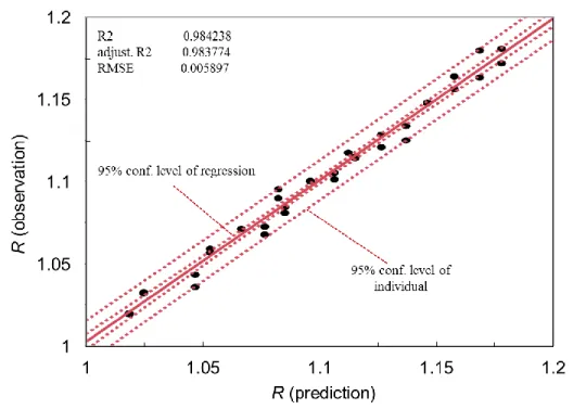
Figure 3.12. Correlation between observation and prediction of normalized sheet 56
resistance (R), indicating very good accuracy of the proposed prediction model.
Figure 4.1. Panels (a) and (b) showing SLG/Cu and bare Cu samples, respectively, 63 and (c) Raman spectra of three random points on SLG surface.
Figure 4.2. Schematic of three parts SE measurement on non-uniform SLG/Cu surface, 65 (b) and (c) sample structure in the basic and advanced models, respectively.
Figure 4.3. Optical constant of mixing composition of C-base film in the basic model. 66 Panels (a) and (b) showing refractive index (n) and extinction coefficient (k), respectively.
Figure 4.4. Optical constant of mixing composition of C-base film in the advanced model. 67 Panels (a) and (b) showing refractive index (n) and extinction coefficient (k), respectively.
Figure 4.5. Optical images of (a-d) SLG/Cu and (e-h) bare Cu surface 68 observed before and after 25, 50, and 100 h of THS test.
Figure 4.6. Cu 2p XPS spectra of SLG/Cu surface measured (a) before and 71 (b) after 100 h of THS test.
Figure 4.7. Cu 2p XPS spectra of bare Cu surface measured (a) before and 68 (b) after 100 h of THS test.
Figure 4.8. Atomic concentration ratios of O to Cu measured by XPS on SLG/Cu 72 and bare Cu surfaces measured before and after 25, 50, and 100 h of THS test.
Figure 4.9. Initial atomic geometry and final atomic geometry of 20 ps. FPMD simulation 73 of O atoms on the top and bottom surfaces of a two-layer graphene structure at 1000 K.
from the basic model of SE.
Figure 4.12. Three main parts of the non-uniform SLG/Cu surface observed by OM: 76 (a) part 1, (b) part 2, and (c) part 3.
Figure 4.13. Ellipsometric parameters fitting based on the generated parameters 77 from the (a) basic and (b) advanced models.
Figure 4.14. Relationship between relative amount of a-C and Cu-oxide thickness 80 from the advanced model of SE.
Figure 5.1. Raman spectra of SLG-coated Cu and bare Cu surfaces after 100 h of THS test. 86 Spectrum of SLG (shiny area) shows small D peak without Cu-oxide peaks.
Dark area of SLG and bare Cu spectra show various peaks of Cu2O and CuO.
Figure 5.2. Structural models of the (a) bare Cu, (b) SLG-coated Cu, and 88 stacking SLG layers as (c) DLG-coated Cu and TLG-coated Cu samples.
Figure 5.3. OM images of (a‒d) bare Cu, (e‒h) SLG-coated Cu, (i‒l) DLG-coated Cu, and 89 (m‒p) TLG-coated Cu surfaces measured before and after different durations of THS test.
Figure 5.4 XPS spectra of (A) Cu 2p and (B) Cu LMM measured on bare Cu and 91 graphene-coated Cu surfaces comparing before and after different durations of THS test.
Figure 5.5 Relative O/Cu atomic concentration ratios of the bare Cu and graphene-coated 93 Cu surfaces measured before and after different durations of THS test.
Figure 5.6 Schematic model showing the formation of a galvanic cell 93 among the defective areas of graphene over the Cu surface.
Figure 5.7. Optimized geometry and energy of water migration through 95 overlapping areas of two SLG sheets.
image of a-C:N layer grown on Cu surface for a-C:N ratios of (b) 90:10 and (c) 70:30.
Figure 6.2. C 1s XPS spectra of different a-C:N ratios; (a) 90:10, (b) 80:20, and (c)70:30 103 and (d) relative atomic concentration ratios of N/C measured on the sample surface.
Figure 6.3. Evolution of normalized sheet resistance (R) measured on the top surface 104 of all samples measured before and after 50 and 100 h of THS test.
Figure 6.4. Optical images observed on the top surface of all samples comparing 105 between before (a)‒(d) and after 100 h (e)‒(h) of THS test.
Figure 6.5. Surface morphology observation by SEM for a-C:N samples 106 comparing between before (a)‒(c) and after 100 h (d)‒(f) of THS test.
Figure 6.6 XPS depth profile of bare Cu after 100 h of THS test, which comprising of 107 C, N, O, Cu, and Si atoms.
Figure 6.7. XPS depth profiles of (a) bare Cu, (b) a-C:N 90:10, (c) a-C:N 80:20, 109 (d) a-C:N 70:30, and (e) the previous report of a-C coating on Cu surface.
Figure 6.8. Cu 2p XPS spectra of (a) bare Cu, (b) a-C:N 90:10, (c) a-C:N 80:20, 110 (d) a-C:N 70:30, and (e) a-C coating on Cu surface measured before and
after each cycle of Ar etching.
Table 1.1. Feature comparison between SM and HDD. 4
Table 2.1. Different Raman mode and their significance. 30
Table 2.2. Binding energies of the chemical bonds for Cu 2p and C 1s in XPS. 31
Table 3.1. Summary of THS test conditions for temperature dependence. 41
Table 3.2. Summary of THS test conditions for humidity dependence. 41
Table 3.3. Relative volume relates to the structural change of Cu and Cu-oxide. 47 Table 4.1. THS test duration at 85℃/85% RH converts to the actual lifetime at 27℃/60% RH. 63 Table 4.2. Thicknesses of Cu-oxide layer and C-based thin films with mixing ratios 75
from the basic SE model.
[Journal papers]
1. P. Gomasang and K. Ueno, “Efficient moisture barrier of nitrogen-doped amorphous-carbon layer by room temperature fabrication for copper metallization,” Jpn. J. Appl. Phys. 59, SLLD03 (2020).
2. T. Murota, T. Mimura, P. Gomasang, S. Yokogawa, and K. Ueno, “Humidity reliability of commercial flash memories for long-term storage,” Jpn. J. Appl. Phys. 59, SLLC01 (2020). 3. P. Gomasang, K. Kawahara, K. Yasuraoka, M. Maruyama, H. Ago, S. Okada, and K. Ueno, “A
novel graphene barrier against moisture by multiple stacking large-grain graphene,” Sci. Rep. 9, 3777 (2019).
4. P. Gomasang, S. Ogiue, S. Yokogawa, and K. Ueno, “Lifetime prediction model of Cu-based metallization against moisture under temperature and humidity accelerations,” Jpn. J. Appl. Phys. 58, SBBC01 (2019).
5. P. Gomasang, T. Abe, K. Kawahara, Y. Wasai, N. Nabatova-Gabain, N. T. Cuong, H. Ago, S. Okada, and K. Ueno, “Moisture barrier properties of single-layer graphene deposited on Cu films for Cu metallization,” Jpn. J. Appl. Phys. 57, 04FC08 (2018).
[International conference papers]
1. P. Gomasang, T. Murota, and K. Ueno, “Nitrogen-doped amorphous-carbon as efficient moisture barrier on copper,” Ext. Abstr. Advanced Metallization (ADMETA) Conference, Tokyo, Japan, October 2019, p. 100.
2. T. Murota, T. Mimura, P. Gomasang, S. Yokogawa, and K. Ueno, “Humidity reliability of commercial flash memories for long-term storage,” Ext. Abstr. Advanced Metallization (ADMETA) Conference, Tokyo, Japan, October 2019, p. 86.
3. P. Gomasang and K. Ueno, “Amorphous-carbon barrier against moisture for copper metallization and effects of CF4 plasma treatment,” Ext. Abstr. International Conference on Solid
moisture barrier in Cu metallization,” Ext. Abstr. Advanced Metallization (ADMETA) Conference, Beijing, China, October 2018, p. 9-2.
5. P. Gomasang, S. Ogiue, S. Yokogawa, and K. Ueno, “Temperature and humidity accelerations to establish lifetime prediction model for Cu-based metallization,” Ext. Abstr. International Conference on Solid State Devices and Materials (SSDM), Tokyo, Japan, September 2018, p. 447.
6. P. Gomasang, S. Ogiue, S. Yokogawa, and K. Ueno, “Oxidation structure change of copper surface depending on accelerated humidity,” Ext. Abstr. IEEE International Interconnect Technology Conference (IITC), Santa Clara, USA, June 2018, p. 112.
7. P. Gomasang, T. Abe, S. Ogiue, H. Ura, S. Yokogawa, and K. Ueno, “High temperature and high humidity accelerations to estimate the lifetime of Cu metallization for LSIs,” Abstr. The 13th International Conference on Ecomaterials (ICEM), Bangkok, Thailand, November 2017, p. 90.
8. P. Gomasang, K. Kawahara, H. Ago, and K. Ueno, “Moisture barrier properties of single-layer and double-layer graphene on Cu film,” Ext. Abstr. Advanced Metallization (ADMETA) Conference, Tokyo, Japan, October 2017, p. 124.
[Domestic conference papers]
1. P. Gomasang, T. Murota, and K. Ueno “Moisture barrier properties of nitrogen-doped amorphous-carbon coating on Cu film surface” 7th Green Innovation Symposium, Tokyo, February 2020, p. 163.
2. P. Gomasang and K. Ueno “Amorphous-carbon barrier against moisture for Cu metallization,” The 80th JSAP autumn meeting, Sapporo, September 2019. p. 15-116.
3. P. Gomasang, K. Kawahara, H. Ago, and K. Ueno, “The improved moisture barrier of graphene coating on Cu film surface,” Tokyo, 6th Green Innovation Symposium, February 2019, p. 95.
1. Silver Poster Award in 7th Green Innovation Symposium held at Shibaura Institute of Technology, February 18, 2020.
CHAPTER 1
INTRODUCTION
1.1. Overview
In the era of information technology (IT), most of the information, including images, music, videos, and books or magazines, is published and preserved in digital form, leading to the rapid growth of the demand for digital data storage. Therefore, various types of storage media have been developed and are expected to be used for the long-term storage of digital data. Electronic data storage devices, known as the semiconductor memory (SM) devices, are being developed to meet the growing needs of consumers. Because of their advantages, these devices have been applied in various electronics and are expected to be used in place of traditional magnetic storage devices for the long-term storage of digital data. Thus, it is important to improve the long-term storage reliability of SM devices.
This work focuses on the improvement of the long-term reliability of copper (Cu) metallization because they have been used as conductive materials in place of conventional Al metallization [1‒4]. The main objective of this research is to prevent the Cu oxidation due to moisture by applying a nanocarbon material coating on the Cu surface as a moisture barrier. This approach has been implemented in this research to reach the goal of long-term protection of the Cu surface from oxidation. This approach is promising regarding the improvement of the long-term reliability of SM devices.
1.2. History of digital data storage
Figure 1.1 shows a typical nonvolatile memory including magnetic, optical, and semiconductor memories. Beginning from the magnetic harddisk drive (HDD) memory, it was developed and launched for the first time over half of a century ago by IBM in 1965 [5]. The HDD can store and retrieve digital data by controlling the magnetization direction of magnetic media. It was developed for operation in personal computers in 1980 [6]. Subsequently, the performances of HDDs have continuously been improved and the areal storage density has been updated based on magnetic recording, which is commonly used for the long-term storage of digital data on desktop computers and computer servers as well as for the preservation of data for external use on portable HDDs.
Subsequently, optical memories were developed to record and transfer digital data in a more convenient way and increase the number of users that can access data storage technology at a cheaper price. Data can be stored on optical discs by means of laser irradiation of a plastic plate coated with an optical recording material. There are various types of optical discs such as compact discs (CDs) including write-once media, read-only memory (CD-ROM) and rewritable media; digital video discs including read-only and erasable types; Blu-ray discs. The CD was firstly launched in 1982 for the distribution of music and was continually developed for other applications [7]. Nowadays, CD-ROMs are rarely used to store computer software because the new generation of laptops does not provide an optical drive.
Figure 1.1. Nonvolatile storage devices
HDD Optical media Semiconductor
In today’s modern electronics, the use of SM devices, also known as memory chips, is rapidly increasing on the entire IT market to meet the demands of digital data storage. The existing design in which several transistors are combined on a single integrated circuit (IC) can be classified into as large-scale integrated (LSI) or very-large-scale integrated (VLSI) memories depending on the number of transistors (>1,000 or >100,000 per chip, respectively). The great evolution of ICs in terms of the size is based on Moore’s law. Nonvolatile SMs can be categorized into two types: mask-programmed read-only memory with data mask-programmed during manufacturing and programmable read-only memory (PROM) with data programmed once by the user. Moreover, two types of erasable PROMs have been developed by using ultraviolet light and electrical charge (EEROM) to erase data. The further development of EEROMs led to the invention of the flash memory, which was introduced in 1980 [8]. The flash memory can be electrically rewritten and erased. At present, it has been widely used in various applications such as in universal serial bus flash drives, secure digital (SD) memory cards used to store data in digital cameras and cellphones, and solid-state drives (SSDs), representing the newest flash memory type used in the new generation of laptops and many other applications.
Based on the comparison between the SM and traditional HDD, the SM overcomes all limitations of the HDD with respect to noise, speed, size, and power consumption, except for the capacity and cost [9]. Because the SM requires no complex mechanical systems to store and access data, it will be easier to read the stored data electrically even the read/write system will be lost in the future like “β-system” in the past magnetic recording. The SM devices are used in a variety of small electronic products because of their small size. However, commercial SM devices are very expensive (per GB) because they are newer and harder to manufacture than traditional HDDs. Based on reports on the life expectancy (LE) of data, HDDs have the LE of ~1–7 years depended on the manufacturer [10,11]. The LE of SM devices, including flash drives and SSDs, measured in terms of the mean time to data loss (MTTDL) is ~10–12 years; subsequently, the data start to evaporate [9,11]. The comparison between the SM and HDD is shown in Table 1.1.
Table 1.1. Feature comparison between SM and HDD
1.3. Cu metallization used in SM devices: background and issues
An IC chip used in SM devices contains numerous layers including the front-end-of-line (FEOL) and back-end-of-line (BEOL) layers, as shown in Fig. 1.2 [12]. The FEOL is the first portion of ICs including individual components, such as transistors, capacitors, resistors fabricated on a wafer. These components are connected to each other through the stacked layer via metal interconnect (Al, Cu, or W) in the BEOL portion of, as shown in Fig. 1.2. This layer includes contacts, metal interconnects, and dielectric layers. The use of Cu as interconnection and bonding pad material in ICs in place of traditional Al has been extensively studied since 1997 to reduce the resistance of BEOL interconnects and improve the electromigration (EM) reliability based on the metals’ higher electrical conductivity and current endurance of Cu [1‒4]. Figure 1.3 shows technology regarding the use of gold wires-Cu pad bonds in an advanced packaging platform [10,11].
Although the storage of digital data on the SMs is becoming more advanced and convenient, the long-term preservation of valuable data is a serious concern. A potential cause of the failures of long-term data storage is Cu oxidation due to moisture [13], leading to an increase in the Cu sheet
Parameter Semiconductor memory (SM) Hard disk drive (HDD)
Record Electrical Magnetic
Recording system Relatively simple Mechanically complex
Speed Faster Slower
Size Smaller/thinner Larger
Power consumption Lower Higher
Cost More expensive per GB Cheaper per GB
Capacity Smaller Bigger
Life expectancy ~10‒12 years
(mean time to data loss)
resistance. To avoid Cu oxidation, an impermeable thinner film coating can be applied to the Cu surface as a moisture barrier.
Figure 1.2. Schematic of a chip cross-section with copper interconnect including the FEOL and
Figure 1.3. (a) Schematic of an LSI package with wire bonding [14] and scanning electron
micrographs showing the (b) top view and (c) the cross section of gold wire bonded to the copper pads [15].
1.4. Overall objective
An impermeable thin film coat on the Cu surface can potentially be used to solve the issues described in the previous section. Nanocarbon materials are promising candidates for such a coat on the Cu surface, which is used to improve the long-term resistance of Cu to oxidation due to moisture. Based on previous reports, research on the improvement of the Cu resistance mostly focused on the reliability during operation such as EM and stress-induced voiding [16,17]. However, the long-term storage reliability has rarely been studied and the resistance to humidity has only been reported for Al metallization.
To improve the long-term storage of SMs and thus preserve digital data for over 100 years, one must study how the Cu oxidation can be avoided. Therefore, the goal of this study is to identify an impermeable thin film coating for the application on the Cu surface to prevent the Cu oxidation. Nanocarbon materials, such as graphene and amorphous carbon (a-C) composite, are the excellent candidates because they have been extensively used in many applications [18‒23]. High-quality large-grained graphene has been adopted to investigate the intrinsic moisture barrier properties for coating on the Cu surface in principle and compare them with a Cu surface without coating. However, the deposition of large-grained graphene requires a high temperature (~1000℃), it is not compatible for the current state of LSI fabrication. Then, the application of a-C composite film, which can be deposited at room temperature, has been studied to achieve the goal. The moisture barrier properties of these materials are investigated and compared with a Cu surface without coating.
These studies provide promising guidelines for the improvement of the long-term reliability of Cu used in advanced SM devices to increase their lifetimes over 100 years for the storage of valuable digital data.
1.5. Review of nanocarbon materials: fabrication and properties
According to the small atomic radius of carbon, nanocarbon materials including graphene and a-C composite, can be used as thin barriers in form of coating on the Cu surfaces. Figure 1.4 shows the different structures of graphene and a-C [24]. Graphene is the first candidate, which is used in this work to protect the Cu surface from oxidation due to moisture because of its impermeability and small atom thickness. Other candidates used in this work are a-C and nitrogen (N)-dope a-C (a-C:N) materials. Although a-C and a-C:N materials do not exhibit a crystalline structure such as graphene, they have been used as diffusion barriers in other applications and are compatible with the thermal budget of the present fabrication process.
Figure 1.4. Structures of graphene and amorphous carbon [24].
1.5.1. Graphene
Graphene is an allotrope of carbon (C) arranged in a two-dimensional layer of the hexagonal lattice (thickness of one C atom is ~0.34 nm). Graphene can be synthesized with various methods including mechanical and chemical exfoliation from graphite, and (thermal) chemical vapor deposition (CVD) from C-containing gas on a catalytic metal surface. [25‒28]. All of synthesis methods have their own advantages and disadvantages depending on the application. The CVD can be used to deposit high-quality graphene films at a relatively high temperature (~1000℃) and ambient or low pressure from various C precursors, such as methane, ethane, and propane, using catalyst metals such as Cu, Ni, and Co [28‒30].
Graphene has been used in various applications due to its excellent properties such as the strength, transparency, and electronic properties, etc. Graphene sheets are stronger than steel based on the comparison of materials with in the same thickness and harder than diamonds [31,32]. Despite their strength, they are very flexible and can be stretched by up to 25% and folded [33]. They are highly transparent with white-light adsorption of only 2.3% [34]. Moreover, they exhibit remarkably high thermal and electrical conductivities [35,36]. It has been reported that the impermeability of graphene film prevents even the diffusion of gases [37].
and higher current endurance against EM compared with Cu [45,46]. It potentially can also be used as an atomically thin barrier against Cu diffusion in Cu interconnects to improve the reliability of time-dependent dielectric breakdown (TDDB) [47].
Based on the fact that they are impermeable and can be used as barriers against gases [37], graphene sheets might be appropriate thin moisture barriers for coating on Cu surfaces to prevent oxidation. Although the high-temperature synthesis approach of graphene is still not compatible with the current BEOL thermal budget, graphene samples with large grains should be deposited at high temperature and investigated to evaluate their potential and principle issues regarding the barrier.
1.5.2. Amorphous carbon and nitrogen-doped amorphous carbon
The a-C is an allotrope of carbon, which form a random network. It contains a mixture composition of diamond-like sp3 and graphite-like sp2 bonds and the hydrogen (H) depending on the fabrication process, leading to difference in its physical properties. Figure 1.5 shows a phase diagram including different a-C types [48]. Based on the ratio of sp2/sp3 bonds in Fig. 1.5, the dominant sp3-hybridized bond has a high resistivity, chemical resistance, optical transparency, and high hardness, but is brittle [49,50]. On the other hand, the dominant sp2-hybridized bond is highly conductive and exhibits properties similar to those observed in graphene.
The a-C layer can be prepared with various methods such as magnetron sputtering from a graphite target, plasma-enhanced CVD, and ion beam deposition. [51‒53]. The sputtered a-C in Fig. 1.5 has an sp2 content of up to 90% (along with sp3) and it can induce properly higher conductivity
than those of other methods. Sputtered a-C has also been reported as a Cu diffusion barrier for advanced Cu interconnects [54].
Thus, it is an interesting candidate that may be used to prevent the Cu oxidation in this research. Because a-C:N can be synthesized at room temperature, it is more appropriate for the current chip fabrication process.
Figure 1.5.Ternary phase diagram showing different amorphous carbon types [44].
1.6. Literature review related to the objective of this research
Regarding the humidity resistance of LSIs, lifetime tests under acceleration conditions was carried out on devices containing Al-based metallization, as shown below. However, there is a lack of lifetime tests of Cu-based metallization and a model for the prediction of the lifetime of Cu metallization against humidity has not been reported yet. Therefore, the Cu oxidation due to moisture should be studied and the Cu reliability against humidity should be improved.
the lifetime extrapolation based on the objective that a model can be fitted all data from the stress conditions less than that of 85℃/85% RH.
Because Cu metallization has been studied for the use in interconnect materials in LSIs, including advanced SM devices [1‒4], one of the most serious concerns regarding the long-term reliability is Cu oxidation, as described in the previous sections. The use of a conductive thin film, such as graphene, coated on the Cu surface as a moisture barrier, has been proposed. By using conventionally synthesized single-layer graphene (SLG) on a Cu foil (CVD method), the application of SLG has been studied, which then was adapted to various fields. Based on the impermeability and stability of graphene, SLG has been reported to be an ultra-thin coating material, which can be used to protect the substrate from corrosion, preserving the efficiency of the product, and even inducing an interface diffusion resistance, as described in the literature below.
● L. Nilsson et al. [60] reported the effectiveness of SLG coating on a platinum (Pt) surface protecting against O2 exposure. Based on experiments and simulations, they also
demonstrated that the SLG layer remains intact, even under harsh conditions of H exposure at 2,000 K (1,727℃) and prevents the direct interaction between the Pt surface and H atoms. ● Y. Zhao et al. [61] reported the efficiency of impermeable and transparent SLG, which was deposited on Cu foil using CVD and transferred to a silver (Ag) surface for optical applications. They reveal that SLG inhibits the corrosion of the Ag surface, including electrochemical reactions in salt and strong oxidizing solutions. The SLG/Ag samples maintained their optical properties under harsh conditions.
● S. Chen et al. [62] for the first time reported the use of graphene directly grown on Cu foil to prevent the oxidation in air after heating at 200℃ for up to 4 h. In addition, they investigated the efficiency of a SLG coat on a Cu surface after exposure to aqueous solution of H2O2. The results indicated that only a few spots of SLG/Cu were attacked after 45 min
suggested further improvement of large-grained and defects-free graphene for the use in nanoelectronic devices.
● M. Schriver et al. [63] reported anticorrosion and antioxidation surface treatments of SLG, which was deposited on Cu foil using CVD, used for Cu and silicon (Si) substrates. They found that SLG provides effective short-term oxidation protection (minutes to hours) for Cu and Si surfaces under heating in atmosphere at 250℃ and 185℃ and low humidity. Based on long-term tests, they found that O2 and H2O infiltrated the graphene through
defects and oxidized or corroded the surface underneath the graphene.
● F. Zhou et al. [64] reported that SLG deposited on Cu foil using CVD can be used for short-term protection from oxidation under an ambient atmosphere at room temperature. They revealed that the SLG-coated Cu foil was inhomogeneous and the SLG grain size only reached a few micrometers. The corrosion of SLG/Cu could be enhanced because of the conductive nature of SLG.
● M. Galbiati et al. [65] reported a comparative real-time study showing the evolution of Cu oxide in SLG/Cu and hBN/Cu foils deposited using CVD. They showed that both graphene and hBN coatings provide good protection against Cu oxidation over the short time (30 min at <250℃), The SLG coating performed better than hBN because of its higher quality. However, the hBN coating eventually outperformed the SLG coating in long-term tests, even if the grain size of SLG was larger than that of hBN. They revealed that the grain size of SLG is too small to inhibit Cu oxidation and that the SLG grain boundary area induces high Cu oxidation during long-term tests.
the mean time-to-fail (MTTF) could be three times improved compared with conventional TaN. The MTTFs of the structure were shorter after reducing the transferred SLG. Moreover, multilayer graphene (MLG) exhibited a worse MTTF than SLG due to the higher density of disorders in MLG. In addition, the use of larger-grained SLG was suggested to further improve the Cu diffusion barrier.
Based on the identification of other conductive materials that can be synthesized at low temperature, a-C and a-C:N materials are interesting candidates.
● B.-S. An et al. [54] reported the barrier performance of a sputtered a-C layer deposited by DC magnetron sputtering on SiO2 in blocking Cu diffusion into the SiO2 substrate during
annealing at 400℃ for 10 h. They reported that a thin a-C barrier layer (0.75 nm) prevents Cu diffusion into the SiO2 layer. The results were confirmed using depth profiles and
transmission electron microscopy (TEM). The results indicate a considerable improvement of the reliability of advanced Cu interconnects.
● M. Stelzer et al. [56] reported the electrical characteristics and reliability of low-temperature sputtered a-C and a-C:N at ~400℃ as interface materials with respect to Si and compare them with those of conventional TiSi‒Si contacts. Moreover, the N doping of a-C provided a lower resistivity and improved the stability of the a-C layer. The tests were conducted on a Schottky diode structure. Because the TiSi contacts had a low thermal stability, they could be degraded at high temperature, especially during electrostatic discharge, leading to the diffusion and migration of TiSi in Si. This study revealed that there were no diffusion of sputtered a-C and a-C:N after 109 of stress pulses. They also
mentioned that the diffusion barrier properties of a-C make it a good alternative interconnect material to phase change material in 3D XPoint memories.
They reported that the F atom formed bonds to the surrounding C atom rather than the N atom due to the electrostatic repulsion between N and F atoms. The results indicated that the diffusion barriers of the F atom passing the N atom are extremely large. These large barriers are mainly due to the electrostatic repulsion between N and F atoms originating from the strong electronegativity of both atoms. These findings revealed that N doping can enhance the diffusion barrier against F atoms leading to the suppression of F diffusion.
1.7. Aim and approach to reach the goal
Before improving the long-term reliability of Cu against oxidation due to moisture for over 100 years, the effects of Cu oxidation on the sheet resistance change were studied for the entire stress range of the temperature-humidity storage (THS) test, ~85℃/85% RH, which is the standard test for electronic packages. The depth profile of the Cu oxidation was obtained using Ar+ etching and X-ray photoelectron spectroscopy (XPS) measurements to study the Cu oxidation characteristics. The change in the sheet resistance due to Cu oxidation was measured and used to formulate a model for the prediction of the Cu lifetime depending on the humidity, which can be applied to study the factors accelerating the Cu oxidation.
Based on the literature review described in the previous section, many researchers indicated the impermeability of SLG deposited on Cu foil using CVD [47,60‒65]. However, the efficiency of high-quality large-grained SLG has not been reported. In this work, the efficiency of large-grained SLG deposited on an epitaxial Cu surface using CVD is demonstrated in principle. Based on THS testing (at 85℃/85% RH for 25 h corresponding to ~100 years at 27℃/60% RH), it was expected that the higher quality and larger grain size of the SLG films will lead to the preservation of larger Cu surface areas compared with the commercial SLG deposition on Cu foils. In addition, a non-uniform SLG sample with a mixed composition of a-C and SLG was investigated to study its effect on the Cu-oxidation by using an ellipsometer after THS testing.
efficient moisture barrier of stacked graphene was investigated after THS testing using XPS measurement and the results were compared with those obtained for SLG/Cu and bare Cu samples.
Because the high-temperature deposition of SLG is not compatible with the current thermal budget of the fabrication process of IC chips, a-C and a-C:N materials deposited at room temperature on the Cu surface were investigated after the THS test to study the moisture barrier properties of these films. Sheet resistance change measurements and surface morphology observations using scanning electron microscope (SEM) were performed. Moreover, XPS depth profiling was carried out to confirm the moisture barrier properties of the layer.
These studies provide guidelines for the improvement of the long-term reliability of Cu metallization used in advanced SM devices.
1.8. Structure of the thesis
This dissertation is divided into seven chapters, as shown in Fig. 1.6, which can be briefly described as follows:
Chapter 1 consists of the general information and background including the history of
digital data storage and critical issues leading to the objective of this research. Explanations of nanocarbon materials, including graphene, a-C, and a-C:N are given. In addition, several previous reports related to the objective are reviewed. The approach to reach the goal of this work is also described in this chapter.
Chapter 2 consists of the detailed explanations of the fabrication processes, tests, and
analysis methods. The fabrication methods, including SLG, stacked SLG, and sputtered C, and a-C:N, used in this research are described. Details of the THS testing and analysis methods, such as Raman, XPS, SEM, TEM, optical microscope (OM), and four-point probe method for sheet resistance measurement, are also provided in this chapter.
Chapter 3 contains the results of the XPS and sheet resistance measurement, which were
performed under various acceleration conditions of temperature and humidity to derive the acceleration parameters for the lifetime prediction model of Cu against oxidation due to moisture.
Chapter 4 consists of the experiments, results and discussion regarding the moisture barrier
properties of high-quality large-grained SLG film coating on the Cu surface after THS test investigated by using OM and XPS. First-principle molecular dynamics simulations and calculations of the activation energy for the diffusion of oxygen (O) atoms through the SLG layer are also described in this chapter. The correlation between the SLG quality and Cu-oxide thickness was determined after the THS test using spectroscopic ellipsometry; a non-uniform SLG film was deposited on the Cu surface.
Chapter 5 comprises the two main experiments, that is, Raman measurement in areas with
oxidized Cu on the SLG/Cu surface, showing that Cu oxidation occurred at SLG grain boundaries, XPS measurements indicating that multiple stacking of large-grained SLG films into DLG and TLG can protect the grain boundaries of the SLG film underneath and thus prevent the Cu oxidation during long-term THS test. The mechanism underlying the improvement of the resistance to oxidation based on first-principles simulations for overlapping graphene films are also described in this chapter.
Chapter 6 consists of the experimental results obtained for the sputtered a-C:N layer, which
can be deposited at room temperature as a barrier against Cu oxidation after THS test. The efficiency of the moisture barrier was investigated using OM, SEM, TEM, and XPS measurements after Ar+ etching to obtain XPS depth profiles. The potential mechanisms of a-C:N layer against O diffusion are also discussed in this chapter.
Chapter 7 summarizes all results of this research. The conclusions are drawn. Future
prospects of this work are also provided.
References
[1] H. B. Lee, J. W. Hong, G. J. Seong, J. M. Lee, H. Park, J. M. Baek, K. I. Choi, B. L. Park, J. Y. Bae, G. H. Choi, S. T. Kim, U. I. Chung, J. T. Moon, J. H. Oh, J. H. Son, J.H. Jung, S. Hah, and S.Y. Lee, Tech. Dig. IEEE Int. Interconnect Tech. Conf., 2007, p. 64.
[2] M. R. Baklanov, C. Adelmann, L. Zhao, and S. De Gend, ECS J. Solid State SC. 4, Y1 (2015).
[3] L. L. Jinzhi, C. Yan, W. Bisheng, L. Xiaomin, F. Chao, H. Younan, Proc. IEEE Int. Conf. on Electronic Packaging Technology (ICEPT), 2018, p. 1546.
[4] Y. L. Cheng, C. Y. Lee, and Y. L. Huang, Copper Metal for Semiconductor Interconnects. Noble and Precious Metals–Properties, Nanoscale Effects and Applications (2018).
[5] T. G. Leary, 305 RAMAC; Random Access Method of Accounting and Control. Manual of operation (International Business Machines Corporation, Santa Clara, CA, 1957).
[6] IBM 3380 Direct Access Storage Description and User’s Guide (International Business Machines Corporation, San Jose, CA, 1981) 2nd Ed.
[7] R. Jones, Data Process. 28, 295 (1986).
[8] Flash Memory Guide (Kingston Technology Corporation, Fountain Valley, CA, 2012). [9] H. Kaneko, T. Matsuzaka, and E. Fujiwara, Proc. IEEE Pacific Rim Int. Symp. on
Dependable Computing (PRDC), 2008, p. 281.
[10] R. D. Weiss, Final report to the National Archives and Records Administration, Delivered by Arkival Tech. Corp. under contract requirement NAMA-01-F-0061, 2002, pp.1‒94. [11] B. M. Lunt, Proc. of Archiving, 2011, p.29.
[12] G. Z. Morgan, An Agile Cause Analysis Using JMP. 2017,
https://community.jmp.com/t5/Discovery-Summit-2017/An-Agile-Cause-Analysis-Using-JMP/ta-p/44067. Accessed 17 Sep. 2020.
[13] S. Yokogawa and K. Kunii, Jpn. J. Appl. Phys. 57, 07MG01 (2018).
[14] T. Uno, T. Oyamada, T. Yamada, and T. Oda, Nippon Steel & Sumitomo Metal Tech. Rep.
117, 3 (2015).
[15] J. N. Aoh and C. L. Chuang, J. Electron. Mater. 33, 300 (2004).
[17] S. Yokogawa, Jpn. J. Appl. Phys. 53, 05GA03 (2014).
[18] S. Syama and P. V. Mohanan, Nano-Micro Lett. 11, 6 (2019).
[19] T. H. Han, Y. Lee, M. R. Choi, S. H. Woo, S. H. Bae, B. H. Hong, J. H. Ahn, and T. W. Lee, Nature Photon. 6, 105 (2012)
[20] A. K. Sundramoorthy and S. Gunasekaran, Trac-Trend. Anal. Chem., 60, 36 (2014). [21] D. Pierleoni, Z. Y. Xia, M. Christian, S. Ligi, M. Minelli, V. Morandi, F. Doghieri,
V. Palermo, Carbon 96, 503 (2016).
[22] B. S. Kwon, J. S. Kim, N. E. Lee, and J. W. Shon, J. Electrochem. Soc. 157, D135 (2010). [23] W. Liu, D. Mui, T. Lill, M. Wang, C. Bencher, M. Kwan, and W. Yeh, Proc. SPIE Int. Soc.
Opt. Eng., 2003, p.841.
[24] M. Noked, A. Soffer, and D. Aurbach, J. Solid State Electrochem. 15, 1563 (2011). [25] M. Cai, D. Thorpe, D. H. Adamsonb, and H. C. Schniepp, J. Mater. Chem. 22, 24992
(2012).
[26] A. A. Green and M. C. Hersam, Nano Lett. 9, 4031 (2009).
[27] X. Li, W. Cai, J. An, S. Kim, J. Nah, D. Yang, R. Piner, A. Velamakanni, I. Jung, E. Tutuc, S. K. Banerjee, L. Colombo, R. S. Ruoff, Science 324, 1312 (2009).
[28] H. Ago, K. Kawahara, Y. Ogawa, S. Tanoue, M. A. Bissett, M. Tsuji, H. Sakaguchi, R. J. Koch, F. Fromm, T. Seyller, K. Komatsu, and K. Tsukagoshi, Appl. Phys. Express 6, 075101 (2013).
[29] J. K. Wassei, M. Mecklenburg, J. A. Torres, J. D. Fowler, B. C. Regan, R. B. Kaner, and B. H. Weiller, Small 8, 1415 (2012).
[30] A. Cabrero-Vilatela, R.S. Weatherup, P. Braeuninger-Weimer, S. Caneva, and S. Hofmann, Nanoscale 8, 2149 (2016).
[31] C. Lee, X. Wei, J. W. Kysar, and J. Hone, Science 321, 385 (2008).
[32] R. Mas-Balleste, C. Gomez-Navarro, J. Gomez-Herrero, and F. Zamora, Nanoscale 3, 20 (2011).
[33] T. Chen, Y. Xue, A. K. Roy, and L. Dai, ACS Nano 8, 1039 (2014).
[35] A. A. Balandin, S. Ghosh, W. Bao, I. Calizo, D. Teweldebrhan, F. Miao, and C. N. Lau, Nano Lett. 8, 902 (2008).
[36] B. Galindo, S. G. Alcolea, J. Gómez, A. Navas, A. O. Murguialday, M. P. Fernandez, and R. C. Puelles, IOP Conf. Ser.: Mater. Sci. Eng. 64, 012008 (2014).
[37] J. S. Bunch, S. S. Verbridge, J. S. Alden, A. M. van der Zande, J. M. Parpia, H. G. Craighead, P. L. McEuen, Nano Lett. 8, 2458 (2008).
[38] R. Mehta, S. Chugh, and Z. Chen, Nano Lett. 15, 2024 (2015). [39] N. T. Cuong and S. Okada, Appl. Phys. Lett. 110, 131601 (2017). [40] H. Shen, L. Zhang, M. Liu, and Z. Zhang, Theranostics 2, 283 (2012). [41] A. N. Banerjee, Glob. J. Nano. 1, 555552 (2016).
[42] D. Prasai, J. C. Tuberquia, R. R. Harl, G. K. Jennings, B. R. Rogers, and K. I. Bolotin, ACS Nano. 6, 1102 (2012).
[43] I. U. Unalan, G. Cerri, E. Marcuzzo, C. A. Cozzolino, and S. Farris, RSC Adv. 4, 29393 (2014).
[44] D. Kongahge, J. Foroughi, S. Gambhir, G. M. Spinks, and G. G. Wallace, RSC Adv. 6, 73203 (2016).
[45] L. Li, Z. Zhu, T. Wang, J. A. Currivan-Incorvia, A. Yoon, H.-S. Philip Wong, Proc. IEEE Int. Electron Devices Meeting, 2016, p.240.
[46] L. Li, Z. Zhu, A. Yoon, and H.-S. Philip Wong, IEEE Electron Device Lett. 40, 815 (2019). [47] L. Li, X. Chen, C. H. Wang, J. Cao, S. Lee, A. Tang, C. Ahn, S. S. Roy, M. S. Arnold, and
H.-S. Philip Wong, ACS Nano 9, 8361 (2015). [48] J. Robertson, Mater. Sci. Eng. R 37 129 (2002). [49] Y. Lifshitz, Diamond Relat. Mater. 8, 1659 (1999). [50] A. C. Ferrari, Surf. Coat. Technol. 180 – 181, 190 (2004).
[51] F. Ferrieu, C. Chaton, D. Neira, C. Beitia, L. P. Mota, A. M. Papon, A. Tarnowka, AIP Conf. Proc. 931, 99 (2007).
[52] S. Aisenberg and R. Chabot J. Appl. Phys. 42, 2953 (1971).
[53] R. Pandiyan, N. Delegan, A. Dirany, P. Drogui, M. A. El Khakani, Carbon 94, 988 (2015). [54] B.-S. An, Y. Kwon, J.-S. Oh, C. Lee, S. Choi, H. Kim, M. Lee, S. Pae, and C.-W. Yang,
[55] J. A. Behan, S. N. Stamatin, M. K. Hoque, G. Ciapetti, F. Zen, L. Esteban-Tejeda, and P.E. Colavita, J. Phys. Chem. C 121 6596 (2017).
[56] M. Stelzer, M. Jung, U. Wurstbauer, A. W. Holleitner, and F. Kreupl, Proc. IEEE Int. Electron Devices Meeting, 2018, p.245.
[57] H. Park, S. Lee, H. J. Kim, D. Woo, S. J. Park, J. M. Lee, E. Yoon, and G. D. Lee, J. Appl. Phys. 125, 155701 (2019).
[58] H. Park, D. Woo, J. M. Lee, S. J. Park, S. Lee, H. J. Kim, E. Yoon, and G.-D. Lee, Sci. Rep. 9, 1 (2019).
[59] D. S. Peck, Proc. IEEE Int. Reliability Physics Symposium (IRPS), 1986, pp. 44. [60] L. Nilsson, M. Andersen, R. Balog, E. Lægsgaard, P. Hofmann, F. Besenbacher,
B. Hammer, I. Stensgaard, and L. Hornekær, ACS Nano 6, 10258 (2012).
[61] Y. Zhao, Y. Xie, Y. Y. Hui, L. Tang, W. Jie, Y. Jiang, L. Xu, S. P. Laua, and Y. Chai, J. Mater. Chem. C 1, 4956 (2013).
[62] S. Chen, L. Brown, M. Levendorf, W. Cai, S.-Y. Ju, J. Edgeworth, X. Li,
C. W. magnuson, A. Velamakanni, R. D. Piner, J. Kang, J. Park, and R. S. Ruoff, ACS Nano 5, 1321 (2011).
[63] M. Schriver, W. J. Gannett, A. M. Zaniewski, M. F. Crommie, and A. Zettl, ACS Nano 7, 5763 (2013).
[64] F. Zhou, Z. Li, G. J. Shenoy, L. Li, and H. Liu, ACS Nano 7, 6939 (2013).
CHAPTER 2
FILM DEPOSITION, TEST, AND METHODOLOGY
2.1. Overview
The main aims of this study were to investigate the Cu-surface oxidation under accelerated Cu-oxidation conditions depending on both the temperature and humidity and demonstrate the moisture barrier properties of graphene and a-C:N respectively, as introduced in the previous chapter, in preventing Cu-oxidation. In this chapter, the research methods are described including the thin-film deposition, which was used for Cu and a-C:N sputtering; CVD of SLG, DLG, and TLG; THS test, and methodological theories.
2.2. Fabrication methods
2.2.1. Substrates cleaning
Two types of substrates were used for the deposition of thin films in this work: SiO2/Si and
Al2O3. To study the Cu oxidation and moisture barrier properties of the a-C coat on the Cu surface,
SiO2/Si was used as sample substrate for the deposition of the Cu film layer. The cleaning procedure
used for the SiO2/Si substrate is described below. To demonstrate the efficiency of SLG in
preventing Cu oxidation, an Al2O3 substrate was used for the growth of an epitaxial Cu layer.
Subsequently, large-grain SLG was synthesized on top of the Cu surface on the Al2O3 substrate after
cleaning by Ago group (Kyushu University).
Cleaning of the SiO2/Si substrate before the deposition of the Cu film:
1) Soaking of the substrate in a liquid containing sulfuric acid (H2SO4):hydrogen peroxide
(H2O2), with a 4:1 volume ratio, and shaking for 10 min
2) Dipping in ultrapure water (twice) to remove chemicals
3) Soaking the substrate in a beaker with ultrapure water and ultrasonication for 5 min 4) Removal of surface water using a N2 gas gun
2.2.2. Magnetron sputter deposition
Magnetron sputter deposition has been widely used for the deposition of thin films of a variety of materials, such as metals, semiconductors, ceramics, and insulators, on different substrates. During the deposition, atoms are ejected from the target surface by bombarding it with Ar+ gas at low pressure. Two magnetron sputtering methods were used in this work: direct current (DC) magnetron sputtering and radio frequency (RF) magnetron sputtering. The schematic diagram of the DC/RF magnetron sputtering system is shown in Fig. 2.1.
The DC magnetron sputtering can be used for all conductive targets. As shown in Fig. 2.1, the negative probe of a DC power supply is connected to the conductive target, which serves as the cathode. The substrate side acts as the anode. In a low-pressure Ar atmosphere, Ar+ ions are generated and accelerated towards the target (cathode) to eject atoms from the target surface. The sputtered atoms move towards the substrate on the opposite side and are deposited, leading to the formation of a thin film on the substrate surface. A magnetic field generated by a permanent magnet can be used to enhance the ion bombardment and sputtering rate of the system.
The advantage of RF magnetron sputtering is that a thin film can be deposited on both conductive and insulating targets. Because the deposition on insulating materials requires a very high voltage to maintain the discharge between the electrodes, it is impossible to use DC sputtering. A high-frequency alternating current (13.56 MHz) is applied between the cathode and anode to provide induce electron oscillation and thus ionizing collisions and a self-sustained discharge (Fig. 2.1). A matching network is used to optimize the power transfer from the RF source to the plasma. Because of the higher mobility of electrons compared with Ar+ ions, the electrons will reach the target surface fast during the positive half-cycle of the AC signal. Subsequently, the target will be negatively self-biased and induce the Ag+ ions to form like a shell in front of the target. These Ar+ ions bombard the target to eject atoms from its surface during the negative half-cycle, which results in the deposition of atoms on the substrate.
Figure 2.1. Schematic diagram of DC/RF magnetron sputtering system [1].
2.2.2.1. a-C, a-C:N, and Cu sputtering on SiO2/Si substrate
Firstly, 100 nm thick Cu was deposited on a SiO2/Si substrate at a power of 300 W in an Ar
atmosphere (~0.6 Pa) using DC magnetron sputtering (Shibaura Mechatronics Co., Ltd., CFS-4EP-LL). Subsequently, a-C was deposited on a Cu surface at a power of 300 W in an Ar atmosphere (~0.6 Pa) using RF magnetron sputtering. In the case of N doping, a-C:N was deposited in an Ar– N2 atmosphere. The a-C and N concentrations were controlled by changing the flow rate of the Ar
and N2 gases. The experiment conditions are described in detail in Chapter 6.
2.2.2.2. Cu sputtering on an Al2O3 substrate in preparation of graphene growth
The sample for the sputtering of Cu on an Al2O3 substrate was prepared by the Ago group
(Kyushu University). A 1000 nm thick Cu film was deposited on an Al2O3 substrate by using RF
2.2.3. Deposition and transfer of SLG
After the fabrication of a Cu film on the Al2O3 substrate, large-grain SLG was deposited by
the Ago group (Kyushu University). The CVD of SLG is similar to the method described in a previous report [2‒4]. After the fabrication of an epitaxial Cu film by sputtering, the sputtered Cu film was inserted into a horizontal quartz tube. The substrate was then heated up and annealed for 40 min at ambient pressure, 1000℃, and a gas flow of H2/Ar. Subsequently, the temperature was
raised from 1000℃ to 1075℃ in 20 min and CH4 gas (10 ppm) was introduced to the quartz tube
for 90 min as a C precursor for the SLG synthesis. The sample was then rapidly cooled down to room temperature by removing the sample holder from furnace with a magnet handle under H2/Ar
flow.
The preparation of stacked graphene layers and transfer of SLG are similar to those described in a previous report [3,5,6] and performed by Ago group (Kyushu University). The transfer of SLG onto SLG/Cu as BLG/Cu is schematically shown in Fig. 2.2. The SLG/Cu surface was covered with polymethyl methacrylate (PMMA) by spin-coating. Thermal tape (Revalpha, Nitto Denko) was attached to the PMMA surface. The Cu film was then dissolved in aqueous FeCl3/HCl solution.
Subsequently, the thermal tape/PMMA/SLG composite was washed with deionized water and transferred onto the surface of another SLG/Cu sample. Finally, the thermal tape and PMMA were removed using acetone, leading to the formation of a BLG film on the Cu surface. Note that the transfer process of TLG or SLG onto the SiO2/Si substrate was the same as that described above for
2.3. Temperature humidity storage test
The temperature and humidity chamber (Fig. 2.3) was used to test the resistance of Cu to oxidation due to humidity under accelerated temperature and humidity conditions. The chamber contains a refrigerator, heater, and humidifier, which were used to create accelerated test conditions. The temperature and humidity chamber (ESPEC, SH-242) is an important apparatus, which was used to conduct the THS test in this work to evaluate the long-term reliability of Cu in terms of protection against oxidation due to humidity. Humidity in terms of % RH is the relative ratio between the actual moisture in the air and amount of saturated moisture at the given temperature. It is a common parameter used when the real effect of humidity is considered. For absolute humidity |RH|, mostly expressed in the unit of g/m3, it refers to the actual moisture present in air, regardless the temperature. In this THS chamber, various temperature and % RH conditions were set. The temperature and humidity were increased to achieve the target conditions, as listed below. A typical temperature–humidity profile (85℃/85% RH) is shown in Fig. 2.4.
1) First, the samples are placed on the grate inside the chamber.
2) To set the THS conditions, the target temperature is divided into 7 steps (starting from ~30℃) and the humidity is divided into 3 steps (starting from step 5, ~65% RH). 3) From steps 1‒6, the operating time is set to 15 min/step. During each step, the
temperature and humidity are continuously increased.
4) The soak time starts at step 7 (required THS test time). The THS test time is set to count down after the target conditions are reached. The samples are soaked under these conditions until the time limit is reached.
2.4. Methodology
2.4.1. Raman spectroscopy
Raman spectroscopy is a practical tool that can be used to quickly measure the vibrational energy modes of molecules. It relies upon the inelastic scattering of photons. When the laser light interacts with molecular vibrations, photon scattering is induced and the energy levels of the scattered photons are shifted up or down. The changes in the energy levels of the scattered photons provide information about the vibrational modes, as shown in Fig. 2.5. In the vast majority of scattering events, laser photons are scattered at the same energy. The incident photons are called “elastic or Rayleigh scattering.” Raman scattering is an inelastic scattering process, which is based on the transfer of energy between the molecule and scattered photon. If the molecule gains energy from the scattered photon, the scattered photon will have a lower energy than the incident photon, resulting in a longer wavelength (“Stokes”). Contrarily, if the scattered photon gains energy from molecules, the final energy state will be lower than the initial state and the wavelength of the scattered photon will be lower (“Anti-Stokes”). The frequency range of the Stokes and anti-Stokes lines is the same. Raman measurements are mostly used to observe the Stokes shift.
Figure 2.5. Energy level diagram showing Rayleigh and Raman scattering (Stokes and anti-Stokes
In this work, Raman spectroscopy was used to measure the characteristics of the graphene film. The Raman spectrum exhibits two main peaks, which are the G and 2D bands at 1587 and 2680 cm-1, respectively. An additional peak, that is, the defect-related D band, appears at ~1350 cm-1 when the carbon lattice has defects.
The G band is located at ~1587 cm-1. The band corresponds to the in-plane vibrational mode
of sp2 hybridized carbon atoms. The increase in the G band intensity is due to the higher number of graphene layers. However, the number of graphene layers is determined by investigating the intensity ratio of the G and 2D bands.
The D band, disorder mode, is located at ~1350 cm-1. It corresponds to the breathing mode
of sp2 hybridized carbon rings. The D band originates from a hybridized vibrational mode associated with defects in the graphene structure or at the graphene edges (disconnection in the carbon network). The intensity of the D band is typically high if the carbon lattice contains many defects, which explains why the D band is generally used to determine the quality of graphene sheets [8].
The 2D band, the second-order D band, is located at ~2680 cm−1. It is the result of a two- phonon lattice vibrational process. It is independent of defects or graphene edges. The intensity of the 2D band is always strong in graphene and can be used to determine the number of graphene layers in comparison with the G band. The relative intensity ratio of the 2D/G bands of SLG is >2 and decreases for multilayer graphene and graphite.
Table 2.1 Different Raman modes and their significance. [8]
Mode Position (cm-1) Significance
G ~1587 The G band originates from the stretching of the C‒C bond in graphitic materials.
D ~1350 This band is associated with defects in the graphene structure or at the graphene edges.
2D ~2680
This is the second-order D band. It is always strong in graphene and can be used to determine the number of graphene layers.
2.4.2. X-ray photoelectron spectroscopy
The XPS is a surface characterization technique used to quantitatively determine the atomic composition at an analysis depth of ~1‒10 nm. The XPS is conducted under ultra-high vacuum conditions (~10−9 mbar). A sample surface is irradiated with monochromatic x-rays, resulting in the emission of photoelectrons with energies that are characteristic of different elements, as shown in Fig. 2.6. During the measurement, the kinetic energy of the electrons that are emitted from the top of the material is recorded and used to create a XPS spectrum. The energies and intensities of the photoelectron peaks are used to identify and quantify the surface elements. The measured kinetic energies can be converted to binding energies by using the equation below:
Eb = Ep – Ek – ϕ (1)
where Eb is the binding energy of the electron, Ep is the energy of the X-ray photons, Ek is the kinetic
energy of the emitted photoelectron, and ϕ is the work function depending on the material and spectrometer.
etching of the a-C:N/Cu surface, depth profiles of the element concentrations of the a-C:N/Cu layers were obtained.
Figure 2.6. Photoemission process in XPS [12].
Table 2.2. Binding energies of the chemical bonds for Cu 2p and C 1s in XPS [13-20].
Binding energy (eV) Bond
![Figure 1.2. Schematic of a chip cross-section with copper interconnect including the FEOL and BEOL layers [12]](https://thumb-ap.123doks.com/thumbv2/123deta/9765899.1849903/24.918.253.716.243.924/figure-schematic-cross-section-copper-interconnect-including-layers.webp)
![Table 2.2. Binding energies of the chemical bonds for Cu 2p and C 1s in XPS [13-20].](https://thumb-ap.123doks.com/thumbv2/123deta/9765899.1849903/50.918.202.761.672.1024/table-binding-energies-chemical-bonds-cu-c-xps.webp)