INVITED PAPER
Special Section on Fabrication Technologies Supporting the Photonic/Nanostructure DevicesAssembly Technologies for Integrated Transmitter / Receiver Optical Sub-Assembly Modules
Keita MOCHIZUKI†a), Tadashi MURAO†, Mizuki SHIRAO†, Yoshiyuki KAMO†, Nobuyuki YASUI†, Takahiro YOSHIMOTO†, Daisuke ECHIZENYA†, Masaya SHIMONO†, Hidekazu KODERA†, Masamichi NOGAMI†,andHiroshi ARUGA†,Members
SUMMARY We have succeeded in developing three techniques, a pre- cise lens-alignment technique, low-loss built-in Spatial Multiplexing op- tics and a well-matched electrical connection for high-frequency signals, which are indispensable for realizing compact high-performance TOSAs and ROSAs employing hybrid integration technology. The lens position was controlled to within±0.3μm by high-power laser irradiation. All com- ponents comprising the multiplexing optics are bonded to a prism, enabling the insertion loss to be held down to 0.8 dB due to the dimensional accu- racy of the prism. The addition of an FPC layer reduced the impedance mismatch at the junction between the FPC and PCB. We demonstrated a compact integrated four-lane 25 Gb/s TOSA (15.1 mm×6.5 mm×5.6 mm) and ROSA (17.0 mm×12.0 mm×7.0 mm) using the built-in spa- tial Mux/Demux optics with good transmission performance for 100 Gb/s Ethernet. These are respectively suitable for the QSFP28 and CFP2 form factors.
key words: hybrid integration, optical sub-assembly, 100 Gb/s Ethernet
1. Introduction
The rapid growth of data traffic due to expansion of the Cloud and content streaming services via the Internet re- quires high-capacity optical transmission systems[1]. To meet this demand, Ethernet transmission systems used for communication within or between data centers are currently moving from 10 Gb/s to 100 Gb/s[2], with 400 Gb/s sys- tems on the horizon[3]. For long-reach applications over 10 km, 100 Gb/s Ethernet (GbE) uses a four-lane 25 Gb/s opti- cal architecture employing a local area network wavelength division multiplexing (LAN-WDM) technique to meet the need for cost reduction and energy saving. In addition, the over-the-top operators (OTTs) which run their own data centers have a strong need for low-cost Ethernet systems.
Several multi-source agreements (MSAs), employing, e.g., coarse WDM (CWDM)[4], parallel single-mode (PSM)[5]
etc., are proposed to relax or avoid the difficulties presented by high-cost LAN-WDM optics.
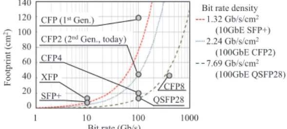
The downsizing of the optical transceivers is proceed- ing in parallel with the development of the transmission sys- tem, as shown in Fig. 1. The centum form-factor pluggable (CFP) standard[6]has been adopted for the first-generation 100GbE transceivers, consisting of four individual 25 Gb/s transmitter optical sub-assemblies (TOSAs) and receiver op- tical sub-assemblies (ROSAs), and an optical multiplexer
Manuscript received June 16, 2016.
Manuscript revised September 16, 2016.
†The authors are with the Mitsubishi Electric Corporation, Kamakura-shi, 247–8501 Japan.
a) E-mail: [email protected] DOI: 10.1587/transele.E100.C.187
(Mux) and demultiplexer (Demux). The bit rate density (the ratio of the bit rate to the footprint) of 0.87 Gb/s/cm2 for the 100GbE CFP is rather smaller than the 1.31 Gb/s/cm2 of the small form factor pluggable plus (SFP+)[7] used for 10GbE. Downsized 100GbE transceivers, CFP2 (2.24 Gb/s/cm2)[6], CFP4 (5.06 Gb/s/cm2)[6], QSFP28 (7.69 Gb/s/cm2)[8] etc., are prerequisite for superseding the current systems. Considering the manufacturing strate- gies for such small form-factors, only integrated opti- cal sub-assemblies (OSAs) can be used to construct such transceivers.
A number of research groups have proposed various OSA structures with several integration technologies which are basically categorized as monolithic and hybrid types.
Mounting four laser diodes (LDs) and an optical Mux, such as a multi-mode interferometer (MMI), on the same indium-phosphide (InP) chip is proposed for the former type[9],[10]. While there is an advantage of simplified as- sembly, this structure involves the difficulty of chip fabrica- tion. For the latter, hybrid, type, an OSA constructed by in- tegrating a planar lightwave circuit (PLC)[11]–[14]or built- in spatial optics with four LDs has been developed[15]–
[17]. For these structures, the optics tend to be complex, reducing the manufacturing yield due to unwanted misalign- ment of the assembly, so a precise alignment technique is essential.
We believe that, while monolithic integration is the ulti- mate solution for ultra-compact, low-cost high-performance OSAs, the hybrid integration approach is the best current so- lution for the immediate productization of an OSA, because developing an assembly is rather easier than developing a chip. In addition, the hybrid integration has the advantages in improving output power of the TOSA and sensitivity of the ROSA compared with the monolithic integration due to
Fig. 1 Bit rate vs. footprint of optical transceivers for 10, 100 and 400GbE.
Copyright c2017 The Institute of Electronics, Information and Communication Engineers
Figure 2 outlines the structures of the four-lane integrated TOSA and ROSA[17]. For the TOSA, four 25 Gb/s electri- cal signals are input from a flexible printed circuit (FPC) and four optical signals are generated at different wavelengths in the 1.3μm band by individual electroabsorption-modulator lasers (EMLs), mounted on a thermos-electric cooler (TEC).
The optical signals modulated at 25 Gb/s are combined in a built-in Mux and launched into an optical output interface.
For the ROSA, the multiplexed 100 Gb/s optical input is di- vided into four independent 25 Gb/s signals in built-in De- mux optics, and the signals are received by a four-lane PD array. The resulting four 25 Gb/s electrical signals are out- put through transimpedance amplifiers (TIAs) and an FPC.
Generally, in order to realize the various characteristics
Fig. 2 Structures in the integrated (a) transmitter and (b) receiver module for 100 Gb/s Ethernet.
3. Precise Lens-Alignment Technique
For conventional single-lane optics, the optical alignment is accomplished by positioning the optical output interface, e.g. a single mode fiber (SMF), receptacle etc., after the EML and lens have been mounted. However, this conven- tional approach cannot be applied to multi-lane optics, be- cause it is necessary to align the lenses after mounting the EMLs and the optical output interface. Figure 3 plots the calculated coupling loss between the EML and the optical output interface as a function of the position of the lens per- pendicular to the optical axis when the positions of the EML and optical output interface are fixed. For comparison, we also show the result for the conventional case as a dashed blue line in the same figure. We assume that the spot size of the EML is 0.83μm and that of the optical output interface is 3.3μm, while the magnification of the lens is 4×to compen- sate for the difference in the spot sizes for each optic. Due to the magnification of the lens, the allowable positional tol- erance of the lens assembly for the multi-lane optics reduces to±0.3μm from±1.5μm for the single-lane optics where the target coupling loss is assumed to be 1.3 dB (the solid line in Fig. 3). The variation of the lens position is usually more than a few microns when it is fixed by laser welding, gluing etc., so that excessive loss due to lens misalignment is normally unavoidable with multi-lane optics.
In order to overcome this problem, we propose a pre- cise lens-alignment technique to control the lens position af- ter the lens misalignment has occurred. To achieve the sub- micron control needed to compensate the misalignment, we cause plastic deformation of the stainless steel of the lens
Fig. 3 Coupling loss as a function of the relative position of the lens and optical output interface, where 0 corresponds to the optimum position.
Fig. 4 (a) Construction of the proposed lens holder for controlling the lens position by high-power laser irradiation. (b), (c), (d) Mechanism for shifting the lens by state-variation of the top surface of the holder in (b)±x, (c)−y, (d)+ydirections calculated by 3D FEM (Quick Welder software).
Blue corresponds to a larger shift in each direction.
Fig. 5 Experimental results for relative position of the lens in they-axis as a function of the number of laser irradiations (9 samples). The gray region indicates the target tolerance of±0.3μm.
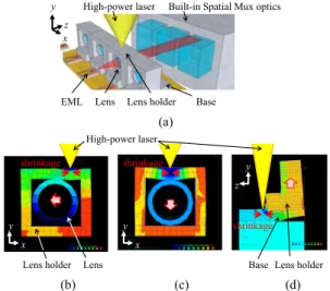
holder by high-power laser irradiation. Figure 4 depicts the concept and principles of the proposed technique. The lens is bonded to the lens holder at the top of the lens. Irradi- ating the top of the holder with a high-power laser, e.g. a YAG laser, causes a state change of the lens holder, induc- ing a compressive stress at the surface, with solidification after melting. The lens holder is thus distorted slightly. We calculate the shift in lens position by the 3-D finite element method (FEM) as shown in Figs. 4 (b)–(d). When the top of the lens holder is irradiated, the bending of the holder shifts the lens in the±xand−ydirections as shown in Figs. 4 (b) and (c). For the+ydirection, we deform the base underneath the lens holder as shown in Fig. 4 (a). If the top of the base is irradiated, the base adopts a downward convex shape. As a result of this deformation of the base, the lens shifts in the +ydirection as shown in Fig. 4 (d). In the proposed method, we can detect the direction and degree in which the lenses should be moved by monitoring the beam angles and posi- tions (e.g., a CCD camera) at the end of the multiplexer.
Figure 5 plots the experimental results for relative lens position in they-axis as a function of the number of laser irradiations. The gray region indicates the target tolerance
Fig. 6 (a) Schematic structure of the narrow lens holder. (b), (c), (d) mechanism for shifting the lens by state-variation of the top surface of the holder or base in (b)±x, (c)−y, (d)+ydirections calculated by 3D FEM (ANSYS Software). Red corresponds to a larger shift in each direction.
of±0.3μm. We put nine lens samples in an initial position +1.7μm away from the optimum position, the thickness of the lens holder being 0.4 mm, the width in thex-axis being 2.8 mm, the depth in thez-axis being1.8 mm and the height in they-axis being 2.6 mm. The position of the lens can be controlled to within the target range of ±0.3μm from the optimum position by less than three laser irradiations with energies of 0.7 J and 0.5 J. The laser power is determined by considering both minimization of the number of irradiations and the degree of shift. The irradiation cycle is not to be limited to three times. The irradiations are carried out until the lens is controlled to be within the target range. These results indicate that the precise lens-alignment technique is fully established[14],[16].
However, it is difficult to apply the proposed technique to a small TOSA complying with a small transceiver form- factor such as CFP4 or QSFP28, because the lens holders limit the ability to downsize the TOSA. To overcome this problem, we developed the new lens holder avoiding side pillars shown in Fig. 6 (a). In order to control the lens posi- tion precisely, we use the same method as previously, irradi- ating the top of the lens holder or the base with a high-power laser, as shown in Figs. 6 (b)–(d). The new lens holder al- lows us to reduce the overall width of the lens-alignment system.
4. Low-Loss Built-In Spatial Mux/Demux Optics The low-loss built-in technique is applied to both OSAs.
However, the Spatial Demux optics for the ROSA requires more precise alignment than the Spatial Mux optics for the
as shown in Fig. 7. The Spatial Demux optics consist of band-pass filters, a mirror, a triangular prism, and a lens array attached together to a small prism 5 mm × 8 mm.
The input light is demultiplexed by multiple reflections be- tween the band-pass filters and the mirror. Each light pass- ing through a band-pass filter is bent towards the PD array by the triangular prism. This array of optics allows us to control the misalignment of the band-pass filters to within
±0.05◦, because the band-pass filters and the mirror, which require the most precise assembly of all the optical compo- nents, are bonded to the accurately shaped prism.
We investigated the relationship between excess inser- tion loss and band-pass filter misalignment in angle and po- sition. Figure 8 shows the calculated contour map of aper-
Fig. 7 Proposed built-in Spatial Demux optics with all optical compo- nents integrated as one block, with the band-pass-filters, mirrors, and lens array attached together to a prism; (a) top view and (b) side view.
Fig. 8 Calculated excess aperture loss with angle and position of the inci- dent light to a band-pass filter. The region enclosed with a red line outlines the target aperture loss of less than 1.0 dB.
In order to estimate accurately the required precision of band-pass filter alignment, we simulated the dependency of the yield ratio on the variation in band-pass filter positioning using the Monte Carlo method (10,000 trials). Figure 9 il- lustrates the distribution of the incident angle and positional errors for the Lane 3 light, assuming that the tilts of the Lane 0, 1 and 2 band-pass filters are random, following a normal distribution with 2σequal to (a) 0.05◦and (b) 0.10◦for each trial. Each point on the map indicates the results of a trial obtained by calculation based on ray tracing. In this simu- lation, the yield ratio of the Demux optics is expected to be 99.93% for case (a) and 94.5% for case (b). We conclude that an assembly accuracy of ±0.05◦ for the band-pass fil-
Fig. 9 Distribution of the incident angle and positional variations on a lens in Lane 3 vs. tilt angles of the band-pass filters using the Monte Carlo method (10,000 trials) where the misalignment error of each band-pass filter is chosen randomly following a normal distribution of 2σequaling (a) 0.05◦and (b) 0.10◦.
Fig. 10 Histogram of angles of band-pass filters attached to a prism for the fabricated built-in Demux optics.
ters is a good target, yielding a low excess loss of 1.0 dB.
Figure 10 is the histogram of the absolute angle of the band- pass filters attached to a prism for the fabricated built-in De- mux optics. The angular precision fully meets the required
±0.05◦[17].
5. Electrical Connection for High-Frequency Signals Coaxial cables and connectors have good high-frequency performance, so they are generally used as the electrical signal interface for the high-frequency signals of an OSA.
However, such electrical interfaces cannot to be used for an integrated OSA because of their large size. The use of FPC instead of coaxial cables and connectors is indispens- able for a compact integrated OSA. The challenge is to min- imize any degradation of the optical waveform due to poor high-frequency characteristics at the FPC interface caused by reflection at its junction with the printed circuit board (PCB).
To overcome this, we propose the new approach to an impedance-matched PCB-FPC connection shown in Fig. 11.
The proposed FPC has three metallic layers, a padding layer, a signal-line layer and a ground layer, whereas a conven- tional FPC has only two metallic layers, a signal-line layer and a ground layer. A 50Ω microstrip transmission line (MSL) is formed on the FPC by the 50μm thick polyimide base material. The PCB has just two layers, a signal layer and a ground layer. An MSL is formed on the PCB using the 250μm thick core material. The FPC is mounted on the PCB such that the FPC’s padding layer faces the PCB’s sig- nal layer. We design the FPC pad to have the same structure as in a conventional 10 Gb/s XMD-MSA module, which has a pad spacingD of 0.79 mm, and a pad widthWP of 0.45 mm. In the junction region, we create a coplanar wave- guide (CPW) with a wide FPC signal track in the signal-line layer and a notched PCB ground pattern as shown in Fig. 12.
With the proposed structure, we can control the impedance by the width of the wide signal track alone. We do not need to change the form of the padding layer. This means that this type of connection enables us to reduce the impedance- mismatch between the PCB and FPC signal lines without compromising the mountability.
We simulated the high-frequency characteristics by the FEM. Figure 13 shows the reflection parameterS11 where
Fig. 11 Structures of (a) PCB, (b) FPC and (c) PCB to FPC connection.
The pink tracks indicate transmission line patterns and the brown tracks in- dicate ground plane patterns. An impedance matched coplanar waveguide is formed at the PCB to FPC connection by introducing a notch in the PCB ground plane and a wide signal track on the FPC.
Fig. 12 Cross section of PCB to FPC connection. The impedance can be controlled by the width of wide signal trackWS.
Fig. 13 Calculated reflection parameterS11of the PCB to FPC connec- tion as a function of frequency for a conventional two-layer FPC and the proposed three-layer FPC.
WSis 0.8 mm, yielding a 50ΩCPW. For comparison, we also show the calculated results for a conventional two-layer FPC. The input and output ports are assumed to be 2.5 mm long 50ΩMSLs formed at the PCB and FPC edges. For the conventional two-layer structure, the maximumS11is worse than 10 dB in the frequency range from 0 to 30 GHz. On the other hand, the proposed three-layer structure improvesS11
to better than 22 dB. These results indicate that the proposed
formed at the rear of the packages without any lead-pins so as to reduce the package width. One of the FPCs is for the high frequency signals and the other is for the DC bias of the EMLs, TEC, PDs and TIAs. The width of the ROSA is due to the four discrete TIAs which were mounted on the base.
6.1 TOSA
Figure 15 shows the measured relative output power spec- trum of the fabricated 100 Gb/s integrated TOSA. The four EMLs are driven simultaneously with an operating cur- rent of 60 mA. The wavelengths of the lanes were 1295.5, 1300.2, 1304.9 and 1309.3 nm, respectively, satisfying the specification of 100 Gb/s Ethernet. The DC output pow- ers of the lanes were+4.40,+4.22, +4.37 and+4.4 dBm, respectively, which enables the average output power to be more than+1.0 dBm with 28 Gb/s non-return to zero (NRZ) modulation of all lanes. The coupling loss for each lane was less than−2.6 dB which included the insertion losses
Fig. 14 Photographs of developed (a) 100 Gb/s integrated TOSA and (b) 100 Gb/s integrated ROSA.
Fig. 15 The relative output power spectrum of the fabricated 100 Gb/s integrated TOSA. The four EMLs are driven simultaneously with an op- erating current of 60 mA. The colored regions indicate the bandwidths of each lane per IEEE802.3ba.
Fig. 16 The fiber output powers depending on the operating currents with the EML temperature of 55◦C and the case temperature of 30◦C.
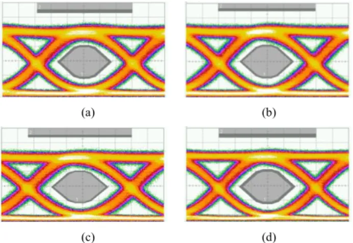
Fig. 17 Four 28 Gb/s waveforms of the fabricated integrated TOSA in a back-to-back configuration for (a) Lane 0, (b) Lane 1, (c) Lane 2 and (d) Lane 3.
using 28 Gb/s PRBS31 (231−1 pseudo-random binary se- quence) NRZ electrical signals with a low voltage of 1.75 Vpeak-to-peak. Clear eye openings were successfully obtained with large mask margins of 15, 12, 11 and 17% for each lane. The extinction ratios were 9.4, 9.1, 9.2 and 9.5 dB, respectively.
6.2 ROSA
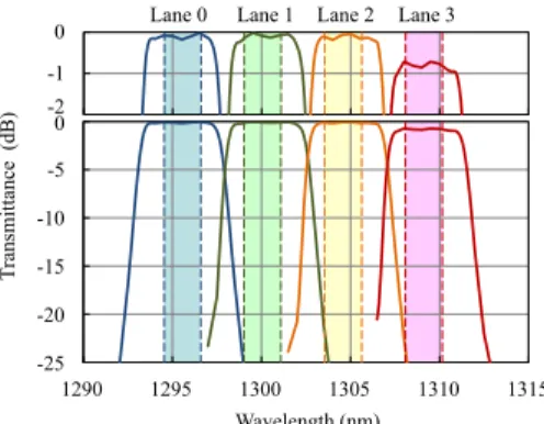
The measured transmittances of the four lanes are plotted in Fig. 18; the lower plot covers 0 to−25 dB, the upper part is a magnified plot covering 0 to−2 dB. These transmittances are evaluated from the received currents of the four-lane PD array normalized by the response of each PD. The adjacent- lane isolation for all lanes was more than 20.0 dB, and the optical losses of Lanes 0, 1, 2 and 3 were 0.21, 0.10, 0.19 and 0.8 dB respectively. The loss of Lane 3 was larger than those of the others. This is due to the aperture loss of the collimated light path to Lane 3, which is the longest.
Figure 19 is the measured bit error ratio (BER). The input optical signal was NRZ modulated with PRBS31 at 25.78125 Gb/s, the extinction ratio being 10.5 dB. The sen- sitivity criterion of IEEE 802.3ba[2] is also marked at the
−10.8 dBm average power level, which is converted from
−8.6 dBm OMA. The average power sensitivities of Lanes
Fig. 18 Measured transmittances of the four lanes evaluated from the received currents of the four-lane PD array normalized by the response of the four-lane PD array.
Fig. 19 BER results for the four lanes with and without adjacent lane signals.
0, 1, 2 and 3 are −13.1,−12.7,−12.1 and−12.7 dBm, re- spectively. Figure 18 also shows each lane’s BER results in the presence of an adjacent lane. The loss of sensitivity due to the crosstalk is less than 0.1 dB. These results indi- cate that the electrical and optical isolation is high enough to suppress the crosstalk.
7. Conclusions
We have developed three assembly technologies for the in- tegrated TOSA and ROSA, a precise lens-alignment tech- nique, low-loss built-in Spatial Multiplexing optics and a well matched electrical connection for the high-frequency signals. This combination of three techniques allows us to realize a compact TOSA 15.1 mm L×6.5 mm W×5.6 mm H, and a compact ROSA 17.0 mm L×12.0 mm W ×7.0 mm H, with good 100 Gb/s Ethernet transmission perfor- mance. They are respectively suitable for the QSFP28 and CFP2 form factors. We expect these assembly technologies will contribute to the realization of the next generation of in- tegrated optical devices for transmission systems operating at 100 Gb/s and over.
References
[1] CISCO, “The zettabyte era –Trends analysis,” White paper, May 2015.
[2] IEEE P802.3ba 40 Gb/s and 100 Gb/s ethernet.
Available: http://www.ieee802.org/3/ba [3] IEEE P802.3bs 400 Gb/s ethernet.
Available: http://www802.org/3/bs/
[4] 100G CWDM4 MSA Technical Specification.
Available: http://www.cwdm4-msa.org/
[5] 100G PSM4 Specification. Available: http://www.psm4.org/ [6] CFP Multi-source Agreement. Available: http://www.cfp-msa.org/ [7] SFF-8431 Specifications for Enhanced Small Form Factor Pluggable
Module SFP+. Available: ftp://ftp.seagate.com/sff/SFF-8431.PDF [8] SFF-8665 Specifications for QSFP+ 28 Gb/s 4X Pluggable
Transceiver Solution (QSFP28).
Available: ftp://ftp.seagate.com/sff/SFF-8665.PDF
[9] T. Fujisawa, S. Kanazawa, Y. Ueda, W. Kobayashi, K. Takahata, A. Ohki, T. Ito, M. Kohtoku, and H. Ishii, “Low-loss cascaded Mach-Zehnder multiplexer integrated 25-Gbit/s×4-lane EADFB laser array for future CFP4 100 GbE transmitter,” IEEE J. Quantum Electron., vol.49, no.12, pp.1001–1007, Dec. 2013.
[10] S. Kanazawa, W. Kobayashi, Y. Ueda, T. Fujisawa, K. Takahata, T.
Ohno, T. Yoshimatsu, H. Ishii, and H. Sanjoh, “30-km error-free transmission of directly modulated DFB laser array transmitter op- tical sub-assembly for 100-Gb application,” J. Lightwave Technol., vol.34, no.15, pp.3646–3652, Aug. 2016.
[11] Y. Beak, Y.T. Han, C.W. Lee, D.H. Lee, O.K. Kwon, J.W. Shin, S.H. Park, and Y.A. Leem, “Optical components for 100G ethernet transceivers,” The 17th Opto-Electronics and Communication Con- ference, 4D1-2, Busan, Korea, July 2012.
[12] T. Ohyama, Y. Doi, W. Kobayashi, S. Kanazawa, K. Takahata, A. Kanda, T. Kurosaki, T. Tanaka, T. Ohno, H. Sanjoh, and T.
Hashimoto, “Compact hybrid integrated 100-Gb/s transmitter op- tical sub-assembly using optical Butt-coupling between EADFB lasers and silica-based AWG multiplexer,” J. Lightwave Technol., vol.34, no.3, pp.1038–1046, 2016.
[13] Y. Doi, M. Oguma, T. Yoshimatsu, T. Ohno, I. Ogawa, E. Yoshida, T.
Hashimoto, and H. Sanjo, “Compact high-responsivity receiver op- tical subassembly with a multimode-output-arrayed waveguide grat-
S. Nishikawa, R. Takemura, M. Nakaji, and A. Sugitatsu, “Four- channel integrated receiver with a built-in spatial demultiplexer op- tics for 100 Gb/s ethernet,” IEICE Trans. Electron., vol.E96-C, no.7, pp.981–988, July 2013.
[18] M. Shirao, N. Ohata, N. Yasui, K. Uto, T. Fukao, T. Hatta, H.
Aruga, and T. Mizuochi, “A 1.55μm 40 Gbps EML TOSA Employ- ing a novel FPC connection,” J. Lightwave Technol., vol.32, no.19, pp.3344–3350, 2014.
Keita Mochizuki received the B.E. de- gree in Electric and Electronic Engineering from Kyoto University in 2006 and M.E. degree in Electronic Science and Engineering from Kyoto University in 2008. In the same year, he joined the Mitsubishi Electric Corp., Japan, where he is currently engaging in the study of optoelectron- ics devices for optical communication. He is a member of the Institute of Electronics, Informa- tion and Communication Engineer (IEICE).
Tadashi Murao was born in Ibaraki, Japan, on December 16, 1982. He received the B.S., M.S., and Ph.D. degrees in media and network technologies from Hokkaido University, Sap- poro, Japan, in 2006, 2008, and 2010, respec- tively. From 2008 to 2011, he was a Research Fellow of the Japan Society for the Promotion of Science (JSPS). He is currently with the In- formation Technology R&D Center, Mitsubishi Electric Corporation, Kanagawa, Japan. His current research interests include the optimiza- tion of optelectronic-device design and theoretical investigation of opti- cal phenomena in band-gap devices, and so on. Dr. Murao is a member of the Institute of Electronics, Information and Communication Engineers (IEICE), and the Institute of Electrical and Electronic Engineers (IEEE).
Yoshiyuki Kamo received the M.E. degree in Material Chemistry and Engineering from Osaka University in 2009. In the same year, he joined the Mitsubishi Electric Corp., Japan, where he is currently engaging in the Develop- ment of Assembly Technology for Communica- tion Devices. He is a member of the Electro- chemical Society of JAPAN.
Nobuyuki Yasui received the B.E. and M.E.
degrees in electronic engineering and system design engineering from Kanazawa Institute of Technology in 1998 and 2000, respectively. In 2000, he joined Mitsubishi Electric Corporation, Japan, where he is currently engaging in the ap- plication of optoelectronics devices for optical communication.
Takahiro Yoshimoto received the B.E. de- gree in Mechanical Engineering from Kyushu Institute of Technology in 2005 and M.E. degree in Mechanical Engineering from Kyushu Insti- tute of Technology in 2007. In the same year, he joined the Mitsubishi Electric Corp., Japan, where he is currently engaging in the study of structural reliability and fracture mechanics for electronic products.
Daisuke Echizenya received the B.E. de- gree in Mechanical Engineering from Hokkaido University in 2000 and M.E. degree in Mechan- ical Engineering from Hokkaido University in 2003. In the same year, he joined the Mitsubishi Electric Corp., Japan, where he is currently en- gaging in the study of design optimization for structure of electronic products.
Masaya Shimono received the B.E. de- gree in Mechanic and Electric Engineering from Tohoku University in 2004 and M.E. degree in Aerospace Engineering from Tohoku University in 2006. In the same year, he joined the Mitsubi- shi Electric Corp., Japan, where he is currently engaging in the study of production engineering.
Hidekazu Kodera received the B.E. degree in Mechanical Engineering from Osaka Univer- sity in 1997 and M.E. degree in Mechanical En- gineering from Osaka University in 1999. In the same year, he joined the Mitsubishi Electric Corp., Japan, where he is currently engaging in the study of production engineering for optical device etc.
Masamichi Nogami graduated from the Toin Technical College, Kanagawa, Japan, in 1986. In the same year he joined Mitsubishi Electric Corporation, Kanagawa, Japan, where he has been engaged in research and develop- ment on fully integrated optical transceivers. He is currently engaging in the study of optoelec- tronics devices for optical communication. He is a member of the Institute of Electronics, Infor- mation, and Communication Engineers (IEICE) of Japan.
Hiroshi Aruga received the B.E. degree in materials science form Tohoku University, Miyagi, Japan, in 1992, and the M.E. degrees in electrical engineering from Sophia University, Tokyo, Japan in 1994. He is with Mitsubishi Electric Corporation, Kanawaga, Japan, work- ing in the field of design and development of mi- crowave components for space satellite and op- tical components for telecommunication system from 1994. He is a member of IEEE Photonics Society and the Institute of Electronics, Infor- mation and Communication Engineers (IEICE).
![Figure 2 outlines the structures of the four-lane integrated TOSA and ROSA [17]. For the TOSA, four 25 Gb/s electri-cal signals are input from a flexible printed circuit (FPC) and four optical signals are generated at different wavelengths in the 1.3 μm ba](https://thumb-ap.123doks.com/thumbv2/123deta/5624244.1500003/2.892.102.404.633.1076/figure-outlines-structures-integrated-flexible-generated-different-wavelengths.webp)