Author(s) Okumura, Hironori
Citation Kyoto University (京都大学)
Issue Date 2012-03-26
URL http://dx.doi.org/10.14989/doctor.k16861
Right
Type Thesis or Dissertation
Textversion author
in AlN Grown on SiC {0001} and
Their Reduction by Initial Growth Control
February 2012
Hironori OKUMURA
Electronic Science and Engineering
Kyoto University
Abstract
AlN, which is a direct transition semiconductor with a wide band gap (6.0 eV), has attracted attention as a material for deep-ultraviolet (UV) light-emitting diodes (LEDs) as well as a underlying template of GaN-based high-electron-mobility transistors (HEMTs). However, existence of high-density extended defects in the AlN heteroepitaxial layers is obstructing realization of superior-performance devices. Improvement of crystalline quality of the AlN layers is a key issue.
For high-quality AlN growth, SiC is one of the most suitable substrates because of the small lattice mismatch between AlN and SiC (∆a ∼0.9%). In AlN growth on SiC, there are two critical issues, i. e., polytype (2H/4H or 6H) and valency (III-V/IV-IV) mismatch. The polytype mismatch generates planar defects, called stacking mismatch boundaries (SMBs), and the valency mismatch enhances a three-dimensional (3D) growth mode, generating a high threading dislocation density (TDD) (∼ 1010 cm−2). The author had attempt to
overcome these problems by controlling SiC-surface structures and initial AlN growth, and achieved high-quality AlN growth (TDD: 4 × 108 cm−2) without SMBs.
In this thesis, high-quality heteroepitaxial growth of AlN on SiC {0001} by molecular-beam epitaxy (MBE) is presented. In addition, extended defects and optical properties of the AlN layers are characterized. The major results obtained in this study are as follows.
Due to the polytype difference, 2H-AlN layers on 4H- or 6H-SiC {0001} with 1-bilayer-high steps have SMBs. By controlling the step height of SiC to one-unit cell, the SMB can be eliminated. In Chapter 3, control of surface structures and chemical compositions of SiC
{0001} is discussed. The author controls the step heights of SiC {0001} vicinal substrates
by H2-gas etching. Through optimization of gas-etching conditions and off-directions of
the substrates, the 6-bilayer-high steps are obtained in the 30 % area of 2-inch 6H-SiC (0001) wafers, while the 3-bilayer-high steps are uniformly formed in the whole area of them. In a similar manner, 6H-SiC (000¯1) with 3-bilayer-high steps and 4H-SiC {0001} with 2-bilayer-high steps are obtained. In addition, the author confirms that an ex-situ HF-chemical cleaning and in-situ Ga deposition-and-desorption process sufficiently remove residual oxygen on 4H- and 6H-SiC {0001} surfaces.
In Chapter 4, crystalline quality of AlN layers on SiC {0001} is improved especially by focusing on initial growth. First, growth conditions of Al-polar AlN on SiC (0001) with controlled step heights are optimized, realizing a layer-by-layer growth mode from 10 to 30 sec after starting AlN growth. In the AlN growth on 6H-SiC (0001) with 3- or 6-bilayer-high steps, the SMBs are not observed, but a high density of TDs (2 × 1010 cm−2) in the AlN
layer, threading dislocation (TD) rows, is generated at the step edges of SiC before growth. For further reduction of TDD in AlN layers on 6H-SiC (0001), an initial growth control is studied. To improve wettability of initial AlN growth, metallic Ga is deposited just before AlN growth. 2-monolayer (ML)-Ga pre-deposition allows early realization of the layer-by-layer growth mode (still not just after the growth) and reduces TDD in the AlN layer-by-layer to 2 × 109 cm−2. Next, a nitrogen-plasma stabilization process for 10 min before growth is
focused on. In in-situ XPS measurements, the author finds that slight active-nitrogen species reach the SiC surface with a closed plasma-cell shutter during its stabilization process. An unintentional nitrogen-exposure before AlN growth is suppressed by starting growth after nitrogen-plasma ignition, achieving the layer-by-layer growth mode from the first AlN layer. The full-width at half-maximum (FWHM) values of the (0002) and (01¯12) ω-scan diffraction peaks are 40 and 41 arcsec, respectively, and TDD in the AlN layers is decreased to 4 × 108 cm−2 (TDD on SiC terrace: 9 × 107 cm−2). And, all impurity concentrations of
Si, C, and O in the AlN layer are reduced to be below 1 × 1018 cm−3.
N-polar AlN growth on 6H-SiC (000¯1) with controlled step heights is also investigated. The N-polar AlN layer has multinucleation growth, resulting in a rough surface. By decreas-ing supersaturation, i. e., nitrogen-plasma power, the smooth surface with a step-and-terrace structure is obtained: RMS roughness is 0.6 nm. TDD is reduced to 2 × 109 cm−2.
In Chapter 5, extended-defect structures, such as SMBs and TD rows generated at the step edges of SiC, are investigated by transmission electron microscopy (TEM). By the addition of a sacrificial oxidation process for SiC substrates with controlled step heights, stacking sequences of the topmost SiC surface can be modified. In the AlN layer on 6H-SiC with the modified 3-bilayer-high steps, SMBs are generated at the step edges of SiC. The SMBs consist of zigzag structures with (¯2110) and (11¯20) planar defects. For example, the (¯2110) SMBs have the displacement vectors of R=1/2[01¯11]. On the other hand, the TD rows consist of many U-shaped dislocation loops, i. e., TD pairs with Burgers vectors of opposite directions. These TD pairs result from dislocations along the step edges of SiC.
Critical thickness of AlN growth on SiC is investigated by x-ray diffraction (XRD), Raman scattering spectroscopy, cathodoluminescence (CL), and TEM. The critical thickness of AlN growth on SiC is estimated to be 3.5 nm by the Matthews-Blakeslee model, while all experimental results show that it is over 700 nm.
In Chapter 6, optical properties of AlN layers on 6H-SiC {0001} are characterized by CL and photoluminescence (PL) measurements. In the AlN layer coherently grown on 6H-SiC (0001), the peak energy of near-band-edge (NBE) emission is high (6.16 eV) at 300 K due to the biaxial strain, and well agrees with theoretical estimation for coherent growth. A donor bound exciton (D0X) peak is clearly separated from a free A-exciton (F X
A) peak in
the PL measurement at 8.8 K. The small FWHM values of the D0X and F X
A lines, which
are 2.7 and 7.1 meV, respectively, are obtained owing to the good crystalline quality. In Chapter 7, a summary of the present work is given, together with the remaining issues to be solved and suggestions for future work.
Acknowledgements
First, I would like to express my deepest gratitude to Professor Tsunenobu Kimoto for his supervision, continuous guidance, and helpful advice. I would like to thank Associate Professor Jun Suda for his continuous guidance concerning experimental details, helpful suggestions, and constructive discussions throughout this work. They also gave me kind encouragement and the opportunity to conduct this research activity freely.
I would like to thank Professor Minoru Suzuki for his kind encouragement through the discussions. I acknowledge Associate Professor Mitsuru Funato for not only his help-ful advice on this dissertation, but also his assistance with transmission electron mi-croscopy (TEM), x-ray diffraction (XRD), and photoluminescence (PL).
I would like to appreciate Assistant Professor Masahiro Horita for maintenance of molecular-beam epitaxy (MBE) as well as his kind instruction of many experiment appara-tuses. I am also indebted to Assistant Professor Yusuke Nishi for maintenance management of whole experiment system. I am very much obliged to Mr. Daisuke Harata, Mr. Hiroki Miyake, Mr. Mitsuaki Kaneko, Mr. Ryosuke Kikuchi, and Mr. Shunsaku Ueta for helping MBE maintenance.
I am truly indebted to collaborative research groups. I would like to appreciate Dr. Christian Kisielowski and Dr. ChengYu Song at the National Center for Electron Mi-croscopy (NCEM) in Lawrence Berkeley National Laboratory (LBNL) and Dr. Petra Specht at University of California, Berkeley for their meaningful comments, the obser-vation technique, sample processing methods, and the image simulation for high-resolution TEM (HRTEM) observation. They and Ms. Jane Cavlina at NCEM gave me the valuable opportunity to learn HRTEM more deeply. I also thank to Professor Yoichi Kawakami, Dr. Ryan G. Banal, Mr. Ryota Ishii, and Mr. Takao Oto at Kyoto University for helpful advices and helping PL measurements. I wish to offer my gratitude to Professor Akinori Koukitu, Associate Professor Yoshinao Kumagai, and Dr. Kazuhiro Akiyama at Tokyo University of Agriculture and Technology for collaborative study on H2 gas-etching rate of SiC surfaces.
I would like to thank Mr. Hiroyuki Kinoshita, Mr. Keiichi Ikeda, Dr. Shin Sasaki, Mr. Taro Nishiguchi, Mr. Toshihiko Hayashi, and Mr. Yoshimitsu Yoshioka from SiXON Ltd., Japan for supplying gas-etched 6H-SiC (0001) substrates.
I thank to all the members of Semiconductor Science and Engineering Laboratory for their kindness and supports: Dr. Atsushi Koizumi, Dr. Gan Feng, Dr. Giovanni Alfieri, Dr.
Hironori Yoshioka, Dr. Katsunori Danno, Dr. Masato Noborio, Dr. Robert Armitage, Mr. Daisuke Horie, Mr. Hiroki Niwa, Mr. Katsuhiko Fukunaga, Mr. Kazuki Yamaji, Mr. Kei Senga, Mr. Koichi Amari, Mr. Kouhei Adachi, Mr. Koutaro Kawahara, Mr. Muneharu Kato, Mr. Naoki Kaji, Mr. Naoki Okimoto, Mr. Naoki Watanabe, Mr. Naoya Morioka, Mr. Ryouhei Kanno, Mr. Ryota Suzuki, Mr. Seigo Mori, Mr. Sho Sasaki, Mr. Shuhei Ichikawa, Mr. Takashi Okuda, Mr. Tatsuya Iwata, Mr. Toru Hiyoshi, Mr. Yibo Zhang, Mr. Yuichiro Hayashi, and Mr. Yuichiro Nanen. I am grateful to secretaries, Ms. Yoriko Ohnaka and Ms. Mizuki Yamada for kindly supporting my daily work.
This work was supported by Grant-in-Aid for Research Fellow (21.5229) from Japan Society for the Promotion of Science (JSPS). This work was also financially supported in part by New Energy and Industrial Technology Development Organization (NEDO), Japan, Kyoto Environmental Nanotechnology Cluster, Japan, and the Global Center of Excellence Program (C09), the Ministry of Education, Culture, Sports, Science, and Technology of Japan.
Finally, I really thanks my parents, my brother, and all my friends for their understand-ing, continuing care, support, and heartfelt encouragement.
February, 2012 Hironori Okumura
Contents
Abstract i Acknowledgements iii Contents v Chapter 1. Introduction 1 1.1 Background . . . 11.2 Properties of Group-III Nitrides . . . 2
1.3 Current Status of Group-III Nitride Devices . . . 2
1.3.1 AlGaN-based deep-UV LEDs . . . 2
1.3.2 GaN-based HEMTs . . . 5
1.4 Heteroepitaxial Growth of AlN . . . 7
1.4.1 Current status of AlN growth . . . 7
1.4.2 Issues of AlN growth on SiC . . . 9
1.5 Outline of Thesis . . . 12
References . . . 12
Chapter 2. Experimental Details of Crystal Growth 17 2.1 Introduction . . . 17
2.2 Molecular-Beam Epitaxy System . . . 17
2.2.1 Vacuum systems . . . 17
2.2.2 Sample holder and sample heating system . . . 19
2.2.3 Effusion cells and radio-frequency plasma source . . . 19
2.3 Experimental Procedures . . . 20
2.3.1 Preparation of SiC substrates . . . 20
2.3.2 Pretreatment and growth procedures . . . 21
2.3.3 Characterization methods . . . 23
Chapter 3. Surface Control of SiC {0001} 27
3.1 Introduction . . . 27
3.2 Step-Height Control of SiC Surfaces . . . 28
3.2.1 Optimization of H2-gas etching condition . . . 28
3.2.2 Discussion . . . 35
3.2.3 Off-direction dependence of step height . . . 37
3.3 Chemical-Status Control of SiC Surfaces . . . 40
3.3.1 Chemical analysis of SiC surfaces after pretreatments . . . 40
3.3.2 Discussion . . . 43
3.4 Summary . . . 43
References . . . 45
Chapter 4. Growth of High-Quality AlN by Initial Growth Control 47 4.1 Introduction . . . 47
4.2 Optimization of AlN Growth on SiC (0001)Si . . . 48
4.2.1 Experimental procedures . . . 48
4.2.2 Growth-temperature dependence . . . 48
4.2.3 III/V-ratio dependence . . . 50
4.2.4 Discussion . . . 52
4.3 Effect of Step Height of SiC (0001)Si on AlN Epilayers . . . 54
4.3.1 Experimental procedures . . . 54
4.3.2 Surface morphology and crystalline quality of AlN epilayers . . . 54
4.3.3 Extended-defect structures in AlN epilayers . . . 56
4.3.4 Discussion . . . 59
4.4 Al and Ga Pre-Deposition just before AlN Growth on SiC (0001)Si . . . 65
4.4.1 Experimental procedures . . . 65
4.4.2 Effect of Al pre-deposition on AlN epilayers . . . 65
4.4.3 Effect of Ga pre-deposition on AlN epilayers . . . 65
4.4.4 Discussion . . . 72
4.5 Avoidance of Nitrogen-Plasma Exposure before AlN Growth on SiC (0001)Si 74 4.5.1 Introduction . . . 74
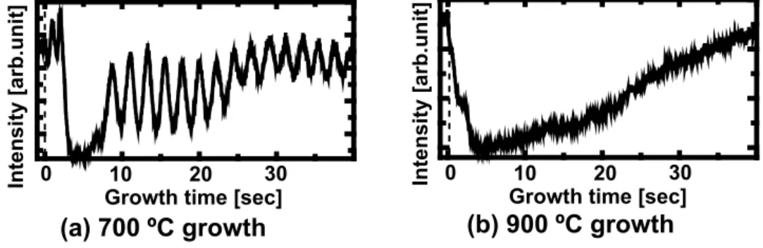
4.5.2 Growth mode at initial growth stage . . . 74
4.5.3 AlN growth just after nitrogen-plasma ignition . . . 76
4.5.4 Discussion . . . 81
4.6 AlN Growth on SiC (000¯1)C . . . 81
4.6.1 Experimental procedure . . . 81
4.6.2 Growth characteristics of N-polar AlN . . . 81
4.7 Impurity Concentration in AlN Epilayers on SiC {0001} . . . 87
4.7.1 Experimental procedures . . . 87
4.7.2 SIMS analysis of AlN epilayers . . . 87
4.8 Summary . . . 91
References . . . 91
Chapter 5. Extended Defects in AlN Epilayers on SiC 95 5.1 Introduction . . . 95
5.2 Characteristics of Stacking Mismatch Boundaries . . . 96
5.2.1 Introduction . . . 96
5.2.2 Experimental procedures . . . 96
5.2.3 Type and density of extended defects . . . 97
5.2.4 Displacement vector of SMBs . . . 97
5.2.5 Discussion . . . 104
5.3 Generation Mechanism of Threading Dislocation Rows . . . 106
5.3.1 Experimental procedures . . . 106
5.3.2 TD structures . . . 107
5.3.3 Generation source of TD rows . . . 107
5.3.4 Estimation of threading dislocation density by XRD . . . 113
5.3.5 Discussion . . . 115
5.4 Critical Thickness of AlN Epilayer on SiC . . . 117
5.4.1 Strain of thick AlN epilayers on SiC . . . 117
5.4.2 Misfit dislocations in thick AlN epilayers . . . 120
5.4.3 Discussion . . . 123
5.5 Summary . . . 126
References . . . 128
Chapter 6. Optical Properties of AlN Epilayers on SiC 131 6.1 Introduction . . . 131
6.2 Violet-Band Cathodeluminescence of AlN Epilayers on SiC . . . 131
6.2.1 Experimental procedures . . . 131
6.2.2 Deep emission band in AlN epilayers . . . 133
6.2.3 Low-temperature measurement of AlN epilayer . . . 133
6.3 Near-Band-Edge Photoluminescence of AlN Coherently Grown on SiC . . . . 136
6.3.1 Peak assignment of low-temperature PL spectra . . . 136
6.3.2 Temperature dependence of PL spectra . . . 139
6.3.3 Discussion . . . 139
6.4 Summary . . . 141
Chapter 7. Conclusions 145 7.1 Conclusions . . . 145 7.2 Future work . . . 147 References . . . 150
Chapter 1
Introduction
1.1
Background
The present all-human society is based on advances in electronics and optoelectronics. In 20th century, semiconductor materials have provided the hardware backbone of the elec-tronics and optoelecelec-tronics. Especially, developments of new semiconductor material have played an important role in evolution of our society and daily lives.
Since germanium (Ge) opened a field of solid state electronics in 1948, many kinds of semiconductor materials have been developed, and their material properties have been maximized for electronic products. In particular, silicon (Si) has provided the foundation of high-speed integrated circuits (ICs) and played a important role to build information technology (IT) society. And, group-III arsenides (GaAs, AlAs, InAs) and group-III phos-phides (GaP, InP) have also provided superior performance as optical devices as well as high-frequency devices. GaAs-based devices, such as infrared/red laser diodes (LDs) in CD/DVD systems and metal-semiconductor field-effect transistors (MESFETs) for power amplifier, are indispensable for our daily lives. However, recently, higher-power microwave devices, and light-emitting diodes (LEDs) and LDs operating at short visible wavelength had been demanded strongly. To fulfill these demands, Si- and GaAs-based materials can not be used due to theoretical limits originating from their material properties, and devel-opment of new semiconductor materials is required. Then, wide bandgap semiconductors, especially gallium nitride (GaN), have attracted much attention.
GaN, which has bandgap of 3.4 eV, is a promising material for frequency and high-power devices due to the excellent property. In addition, not only GaN but also other group–III nitrides (III–Ns) (aluminum nitride (AlN) and indium nitride (InN)) are the most promising materials for the optical devices operating at wavelength of visible range. Last two decades, there have been extensive research and development of GaN-based LEDs and LDs.
1.2
Properties of Group-III Nitrides
The physical properties and material parameters of GaN and AlN are listed in Table 1.1 and Table 1.2, respectively. III–Ns are III-V compound semiconductors composed of tetrahe-drally bonded cation and anion atoms in a closed-packed structure. These alloys crystallize in a wurtzite structure as a thermodynamically stable structure [1]. The III–Ns have at-tracted much attention as the candidates for LEDs 1 [2], because these compounds are
direct-transition-type semiconductors 2 [3]. The III–Ns can cover continuously from 0.7 eV
(bandgap of wurtzite InN) to 6.0 eV (bandgap of wurtzite AlN) by appropriate alloying, as shown in Fig. 1.1.
Applications of the III–Ns are not limited to LED and LDs. In comparison with other semiconductor materials, GaN has high breakdown field, high thermal stability, and high electron saturation velocity (Table 1.1). From these excellent properties, GaN is also used as electronic devices. Using GaN and its alloys with AlN and InN, we can utilize hetero-junctions, i. e., bandgap engineering, expanding the design of device structures, such as high-electron-mobility transistor (HEMT) and heterojunction bipolar transistor (HBT). In particular, GaN-based HEMTs have attracted attention as high-power and high-frequency devices.
1.3
Current Status of Group-III Nitride Devices
In the III–N devices, recently, AlGaN-based deep-ultraviolet (UV) LEDs and GaN-based HEMTs have attracted much attention. In this section, current status of these devices is described.
1.3.1
AlGaN-based deep-UV LEDs
Recnetly, high-Al-content AlGaN deep-UV LED operating at the shorter wavelength (400– 220 nm) attracts much attention for high-density optical data storage, sterilization, chemical analysis, and illumination lamps. Taniyasu et al. demonstrated AlN deep-UV LEDs oper-ating at 210 nm (i. e., the shortest wavelength among III–Ns) under current injection [4]. However, devices based on the AlGaN active layers have much lower efficiency than the InGaN-based devices; for instance, the external quantum efficiency (EQE) of LEDs operat-ing at 285–240 nm is limited to 1% and that of the AlN LED is 10−6% [4–10]. One of the
factors is the high density of threading dislocations (TDs) originated from the heteroepi-taxial growth of AlN or AlGaN. The AlN or AlGaN growth with a smooth surface and low defect density is a requisite to realize high-efficiency devices.
1Excitons are capable of stable existence in GaN due to the large binding energy of 28 meV than the
thermal energy of room temperature (RT).
2Zinc-blende AlN is theoretically expected to have an indirect bandgap. The indirect bandgap of
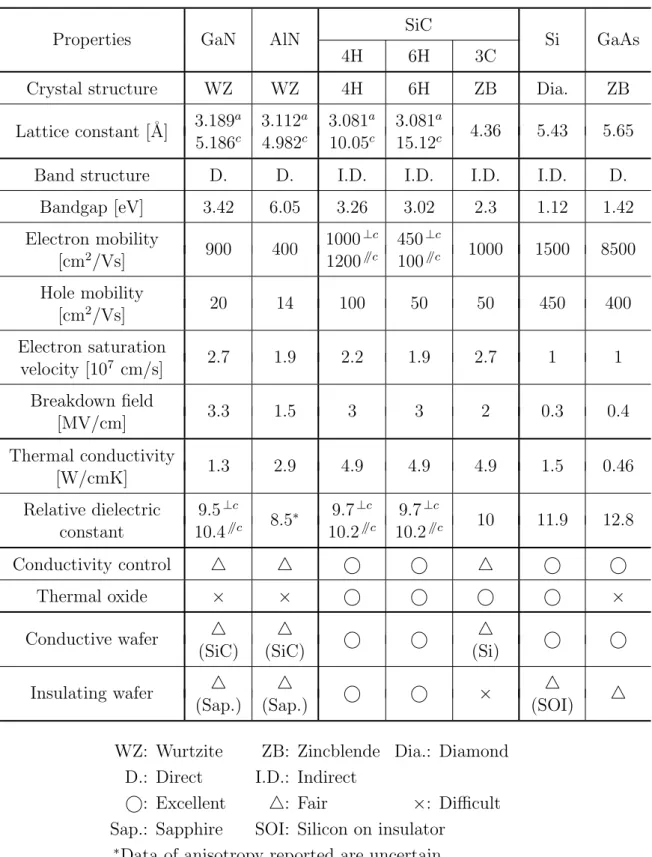
Table 1.1: Physical properties of GaN, AlN, SiC and most common other semiconductor materials.
Properties GaN AlN SiC Si GaAs 4H 6H 3C
Crystal structure WZ WZ 4H 6H ZB Dia. ZB Lattice constant [˚A] 3.189a 3.112a 3.081a 3.081a 4.36 5.43 5.65
5.186c 4.982c 10.05c 15.12c
Band structure D. D. I.D. I.D. I.D. I.D. D. Bandgap [eV] 3.42 6.05 3.26 3.02 2.3 1.12 1.42 Electron mobility 900 400 1000⊥c 450⊥c 1000 1500 8500 [cm2/Vs] 1200//c 100//c Hole mobility 20 14 100 50 50 450 400 [cm2/Vs] Electron saturation 2.7 1.9 2.2 1.9 2.7 1 1 velocity [107 cm/s] Breakdown field 3.3 1.5 3 3 2 0.3 0.4 [MV/cm] Thermal conductivity 1.3 2.9 4.9 4.9 4.9 1.5 0.46 [W/cmK] Relative dielectric 9.5⊥c 8.5∗ 9.7⊥c 9.7⊥c 10 11.9 12.8 constant 10.4//c 10.2//c 10.2//c Conductivity control 4 4 ° ° 4 ° ° Thermal oxide × × ° ° ° ° × Conductive wafer 4 4 ° ° 4 ° °
(SiC) (SiC) (Si)
Insulating wafer 4 4 ° ° × 4 4
(Sap.) (Sap.) (SOI) WZ: Wurtzite ZB: Zincblende Dia.: Diamond
D.: Direct I.D.: Indirect
°: Excellent 4: Fair ×: Difficult
Sap.: Sapphire SOI: Silicon on insulator
Table 1.2: Typical material parameters for GaN, AlN, and SiC. Properties GaN AlN 6H-SiC Elastic stiffness [GPa]
C11 390 [13] 396 [13] 501 C12 145 [13] 137 [13] 111 C13 106 [13] 108 [13] 52 C33 398 [13] 373 [13] 553 C44 105 [13] 116 [13] 163
Deformation potential [eV]
a − D1 -4.9 [13] -6.9 [14]
a − D2 -11.3 [13] -15.2 [14]
D3 8.2 [13] 8.3 [14] D4 -4.1 [13] -4.15 [14]
Phonon deformation potential [cm−1]
aλ for E2h -740 [15] -877 [15] bλ for E2h -727 [15] -911 [15]
Poisson ratio ν 0.20 0.20 0.085 Young’ modulus E(0001) [GPa] 360 330 540 Biaxial modulus Y (0001) [GPa] 480 470 600
c-axis lattice constant (c/n) [Å] a-axis lattice constant [Å]
2.4 2.6 2.8 3.0 3.2 3.4 3.6 B and g ap ener g y [eV ] 0 2 4 6 W av eleng th [nm ] 800 600 400 200 1000 W av eleng th [nm ] 800 600 400 200 1000 B and g ap ener g y [eV ] 0 2 4 6
(a)
(b)
AlN AlN GaN GaN InN InN 4H-SiC 6H-SiC 4H-SiC 6H-SiCFigure 1.1: Relationships between bandgap and (a) a-axis / (b) c-axis lattice constant for hexagonal III–Ns and SiC. Dashed lines show lattice constants of 4H-SiC.
1.3.2
GaN-based HEMTs
Properties of GaN-based HEMTs
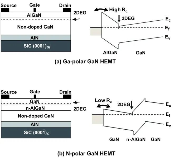
As applications in III–Ns high-power and high-frequency electronic devices, AlGaN/GaN HEMTs attract much attention. In the HEMTs, a strong built-in electrostatic field can exist in the h0001i direction because the noncentrosymmetric nature of the wurzite structure generates spontaneous and piezoelectric polarization [11, 12]. These internal fields form two-dimensional electron gas (2DEG) near an AlGaN/GaN heterointerface, as shown in Fig. 1.2. This electron channel layer near the heterointerface permits a short gate length, improving the high-frequency property in a microwave band. The 2DEG density in AlGaN/GaN is one order of magnitude higher than that in AlGaAs/GaAs, achieving high-current handling capability. A electron mobility of the 2DEG is higher than that of bulk because of no ionized-impurity scattering, realizing the high-speed performance. As listed in Table 1.1, GaN shows approximately one order higher-breakdown field than that of GaAs. High-voltage operation enables the highly-efficient performance. Consequently, GaN-based HEMTs are the most promising for future applications in high-power and high-frequency electronics.
Current status of GaN-based HEMTs
Most of the AlGaN/GaN HEMTs have been fabricated on (0001) or Ga-polar orientation, which is superior in terms of crystalline quality. The Ga-polar AlGaN/GaN HEMTs have already achieved high performance. Recently, research on (000¯1) or nitrogen-polar (N-polar) orientation also attracts much interest due to its strong electron confinement and low contact resistance (Fig. 1.2 (b)) [16–20]. However, both Ga-polar and N-polar AlGaN/GaN HEMTs have too low reliability to be in practical use. One of the factors is a high density of TDs in the GaN films, 108–109 cm−2 [21–23]. High-quality GaN growth is a key issue to realize
high reliability in the AlGaN/GaN HEMTs.
Substrates for GaN-based HEMTs
For high-quality GaN films, using GaN substrate, i. e., homoepitaxial growth, is the most suitable. Although bulk GaN and AlN is available now, high-quality and large-area wafers are unachieved at a reasonable cost. Heteroepitaxial growth of GaN on foreign substrates is inevitable. Among foreign substrates, sapphire (Al2O3) and Si are candidates
for GaN growth, because large-area Al2O3 and Si wafers are commercially available at a
low cost. However, GaN films on Al2O3 and Si are highly defective due to the large lattice
mismatches more than 14%. Additionally, Al2O3 and Si substrates have a problem with a
heat dissipation of the high-power devices owing to the low thermal conductivity. Then, silicon carbide (SiC) has been studied as a suitable substrate for GaN-based high-power devices owing to its excellent thermal conductivity as well as its close lattice constant (∆a ∼ 3.5%). Recently, 4-inch SiC wafers are available at a reasonable cost.
(a) Ga-polar GaN HEMT
(b) N-polar GaN HEMT
AlGaN Non-doped GaN AlN SiC (0001) Gate Source Drain GaN Non-doped GaN AlN SiC (0001) Gate Source Drain n-AlGaN
Low R
cGaN n-AlGaN GaN
High R
c AlGaN GaN 2DEG 2DEG Ec Ef Ev Ec Ef Ev Si C 2DEG 2DEGFigure 1.2: Basic device structures and band diagrams of (a) Ga-polar and (b) N-polar GaN HEMTs.
SiC is a IV-IV compound semiconductor with Si and carbon (C) atoms with the ratio of unity and has more than 200 kinds of polytypes: the difference in stacking sequences along a hexagonal h0001i direction brings various crystal forms. Considering the Si-C pair as a sphere, there are three possible occupation sites denoted by A, B, and C (Fig. 1.3). In their polytypes, now, bulk SiC with 4H (ABCB) and 6H (ABCACB) structures3are commercially
available (Fig. 1.4). The 4H- and 6H-SiC have high crystalline quality (threading dislocation density (TDD) less than 104 cm−2) and conductivity control, such as n-type, p-type, and
semi-insulating (SI). The SI substrate with high resistivity is effective to reduce a leak current and parasitic capacitance in high-power and high-frequency devices.
Above all, {0001} faces can have strong polarization-induced fields parallel to the h0001i direction in the strained layers and have an advantage in 2DEG of HEMTs. In GaN growth on SiC, the GaN films have the same crystal faces as the SiC substrate: i. e., GaN films on SiC (0001) and (000¯1) have Ga polarity and N polarity, respectively [24–27]. Therefore, 4H- and 6H-SiC {0001} SI substrates are suitable for the GaN-based HEMTs.
GaN growth on SiC (0001)
For GaN growth on SiC, an AlN buffer layer is usually used because of the small lattice mismatch between AlN and SiC (∆a ∼ 0.9%). Although a nucleation layer (NL) of AlN can enhance an annihilation of TDs in the GaN films, the TDD in the GaN films have not be reduced to less than 108 cm−2 because the annihilation is limited to TDs close to each
other. Then, the author has proposed a high-quality AlN template as an underlying layer of the GaN growth. The AlN templates with TDD under than 108 cm−2 would allow the
GaN films to have higher crystalline quality. In this thesis, high-quality AlN growth on SiC
{0001} substrates is presented.
1.4
Heteroepitaxial Growth of AlN
1.4.1
Current status of AlN growth
MOCVD growth
High-quality heteroepitaxial growth of III–Ns has been accomplished via metal-organic chemical vapor deposition (MOCVD) techniques. AlN films are also generally grown by MOCVD, but have a high TDD of ∼ 1010 cm−2.
The most popular technique to reduce the TDD is epitaxial lateral overgrowth (ELO), which can annihilate or trap the TDs in a plane normal to the surface direction of the
3H for hexagonal, C for cubic, and R for rhombohedral. Wurtzite and zinc-blende structures are referred
A A A A A A A A A A C C C B B B <1100> <1120> <0001>
Figure 1.3: Hexagonal closed packing of Si–C or III–N pairs.
[0001] <1100> A B A B A B A B A B A B A A B C A B C A B C A B C A B C A B C A A B C A B C C B A B C B A B C B A B C A B C A C B A B C A C B A A C B A C B A C B A C B A : C / N : Si / Al, Ga, In
(a) 2H (Wurtzite) (b) 4H (c) 6H (d) 3C (Zincblende)
Figure 1.4: Stacking orders along [0001] (c-axis) for (a) 2H-, (b) 4H-, (c) 6H- and (d) 3C-structures of SiC or III–Ns.
substrate. However, remarkable reduction of the TDD by ELO is unexpectable because the dislocation bending is difficult in the AlN films . Taniyasu et al. reported that three-dimensional (3D) growth mode at an initial growth stage generated a high TDD, but the propagation direction of the dislocations could change horizontally due to larger-nuclei coalescence in thick growth, resulting in annihilation of the TDs [28]. Imura et al. reported that the annihilation of TDs was enhanced by generating the larger-nuclei coalescence at high growth temperature above 1300◦C, achieving TDD of 108−109 cm−2 [29, 30]. However,
the TDD in the AlN layers has not be reduced to less than 108 cm−2because of the limitation
of the annihilation of TDs. To reduce further TDD, the two-dimensional (2D) growth mode from an initial growth stage is thought to be effective. Banal et al. enhanced Al adatom migration and the 2D growth mode by using a modified migration enhanced epitaxy (MEE), which is characterized by a combination of simultaneous source supply and conventional MEE, realized high-quality AlN growth on Al2O3 substrates [31]; FWHM values of (0002)
and (01¯12) ω-scan diffraction peaks were 38 and 250 arcsec, respectively.
In most of the AlN growth by MOCVD, Al2O3 substrates have been used. The author
expects that AlN growth on SiC (0001) substrates can enhance further the 2D-growth mode due to the small lattice mismatch, improving the crystalline quality of the AlN layer.
MBE growth
Molecular-beam epitaxy (MBE) has an advantage of the 2D-growth mode at an initial growth stage because of a growth control at an atomic level and in-situ observation of the growth mode. In the previous study from our group, AlN growth on SiC (0001) by plasma-assisted MBE (PAMBE) achieved the layer-by-layer growth mode by optimization of the growth condition and control of the SiC-surface structure [32]. The full-width at half-maximum (FWHM) values of the (0002) and (01¯14) ω-scan diffraction peaks were 75 and 518 arcsec, respectively. The author considers that there is still room to improve the AlN-film quality, because no reflection high-energy electron diffraction (RHEED) intensity oscillation was observed at a very initial growth stage, indicating a 3D growth mode occurred just after starting AlN growth. In this thesis, the author tries to improve the crystalline quality of AlN growth by focusing on the AlN/SiC interface.
1.4.2
Issues of AlN growth on SiC
AlN growth on SiC has three kinds of mismatch; (a) polytype, (b) valency, and (c) lattice mismatches. These are factors generating extended defects. For the high-quality heteroepi-taxial growth of AlN, these systems must be overcome.
(a) Polytype mismatch
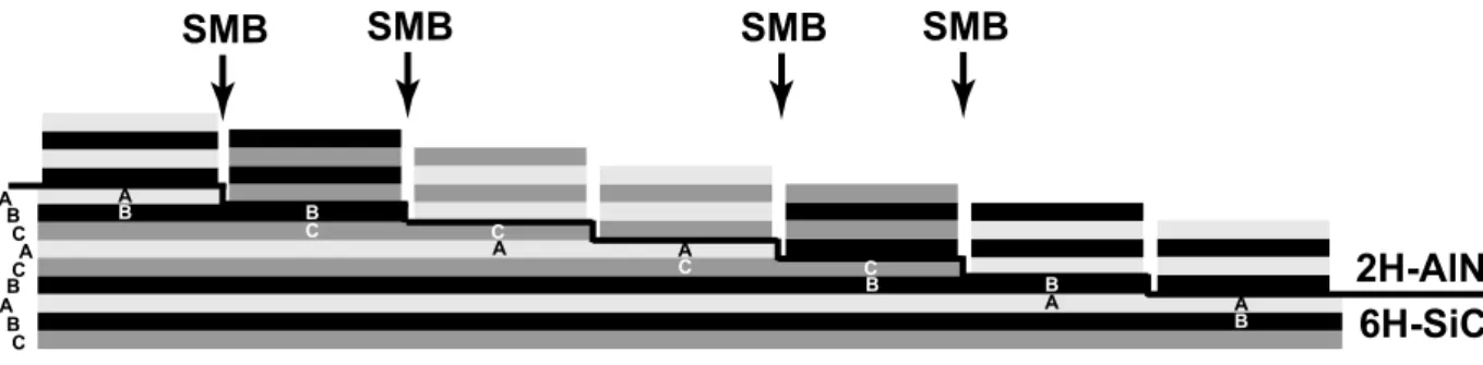
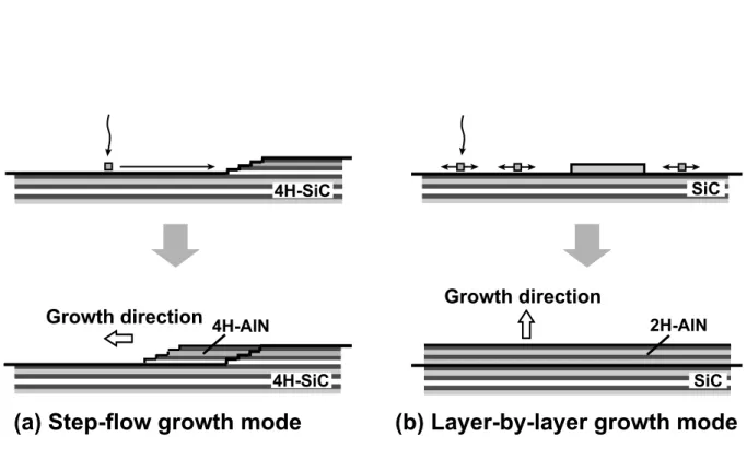
AlN has a wurtzite (2H) structure (ABAB...), but the available SiC wafers have a 6H (ABCACBABCACB...) or 4H (ABCBABCB...) structure. The AlN layer follows stacking sequences of the topmost two bilayers of the SiC surface [33], i. e., if the 6H-SiC surface ter-mination is ABCACBA..., 2H-AlN layers have the stacking sequence ...ABAB. In general, SiC substrates before growth are treated by chemical mechanical polishing (CMP), forming 1-bilayer-high steps. The surface termination of SiC with 1-bilayer-high steps changes on every adjacent terrace because 6H-SiC have six-type terminations (Fig. 1.5). AlN layers on the SiC substrates have different stacking sequences on each terrace of the SiC surfaces and generate planar defects threading the AlN layers, called stacking mismatch bound-aries (SMBs) or prismatic stacking faults (PSFs) [34, 35]. The schematic figure of stacking sequences in 2H-AlN growth on 6H-SiC with 3-bilayer-high steps is shown in Fig. 1.6. SMBs are {11¯20} planar defects generated at step edges of the SiC surface.
Step height of the 6H-SiC surface can be controlled to be 6 bilayer (full-unit-cell height) or 3 bilayer (half-unit-cell height) by high-temperature H2-gas etching via
micro-step-bunching mechanism [36]. 2H-AlN on 6H-SiC substrates with 1- and 3-bilayer-high steps forms SMBs, while we can expect that the AlN layer on 6H-SiC with 6-bilayer-high steps grows without SMBs due to the identical stacking sequences on adjacent terraces. In this thesis, the author attempts to control step heights of the SiC surface with high uniformity and realizes AlN growth without SMBs.
(b) Valency mismatch
AlN is a III-V compound semiconductor, but SiC is a IV-IV compound semiconductor. The most favorite atomic arrangements at an abrupt interface between AlN and SiC {0001} are intermixed configurations of Si-N or Al-C bonds [37]. AlN growth on SiC {0001} with this heterovalent system has much interface energy of the epilayer/substrate, resulting in a 3D growth mode, i. e., generation of numerous defects.
For high-quality AlN growth, a 2D growth mode, especially a layer-by-layer growth mode, from the first layer is required. to reduce the TDD, the author tries to control initial growth of AlN.
(c) Lattice mismatch
There is a lattice mismatch between AlN and SiC (∆a ∼ 0.9%, ∆c ∼ 1.0%) (Fig. 1.1). The critical thickness of AlN growth on SiC is estimated to be 3.5 nm by Matthews-Blakeslee model [38]. In the growth over the critical thickness, a high density of misfit dislocations, which can convert into TDs, are generated owing to the lattice relaxation.
To suppress the generation of the misfit dislocations, the author attempts to increase the critical thickness of AlN growth on SiC by controlling growth conditions, such as the growth temperature, TDD, and growth mode.
A A A B C C C B B SMB 6H-SiC 2H-AlN A A B B C C A C C B B A A B SMB SMB SMB
Figure 1.5: Schematic figure of stacking sequences in topmost two layers of 6H-SiC (0001) substrate with 1-bilayer-high steps.
2H-AlN
3 bilayerSMB
A BC A C B A B C B AB A[0001]
<1100>
<1120>
6H-SiC
Figure 1.6: Schematic figure of stacking sequences in 2H-AlN grown on 6H-SiC (0001) substrate with 3-bilayer-high steps.
1.5
Outline of Thesis
In this thesis, high-quality heteroepitaxial growth of AlN on SiC {0001} by MBE is studied. Extended defect and optical properties of the AlN layers are characterized. The contents of this thesis are as follows.
In Chapter 2, MBE system and characterization methods are described. Typical AlN growth and pretreatment procedures for SiC substrates are also explained.
In Chapter 3, controls of surface status of SiC {0001} vicinal substrates are described. Step heights of 4H- and 6H-SiC {0001} are controlled to half- or one-unit-cell-high steps by micro-step-bunching phenomena in H2-gas etching. Off directions as well as gas etching
conditions are optimized to obtain the step heights with high uniformity at a large area. In addition, removal of residual oxygen on SiC {0001} surfaces by using ex-situ HF-chemical and in-situ Ga deposition-and-desorption process is presented.
In Chapter 4, realization of high-quality AlN growth by three methods (i)-(iii) is de-scribed: (i) step height control of SiC, (ii) group-III metal deposition just before growth, and (iii) avoidance of unintentional active-nitrogen exposure before growth. For (i), growth conditions of AlN layers on 4H- and 6H-SiC (0001)Si with controlled step heights are
opti-mized. And, an impact of the step heights (1, 3, or 6 bilayers) of 6H-SiC (0001) surfaces on the AlN layers is explained. For (ii), to reduce the AlN/SiC interface energy, deposition of metal Al or Ga just before AlN growth is proposed. Effects of deposited Al or Ga on the AlN layers are investigated. For (iii), the impact of an unintentional active-nitrogen expo-sure just before AlN growth is discussed. The chemical status of the SiC surfaces during a nitrogen-plasma stabilization process before growth is investigated, and an optimum growth process is proposed. Using these methods (i)-(iii), the layer-by-layer growth mode from the first layer and reduction of a TDD are successfully realized. In addition, N-polar AlN grown on 6H-SiC (000¯1)C is presented. Impurity concentrations in AlN layers with various growth
conditions, such as different crystalline quality, growth temperature, and polarity, are also studied.
In Chapter 5, extended-defect structures, such as SMBs and TDs, in the AlN layers on 6H-SiC (0001) are described. The author tries to clarify generation mechanism of the SMBs and TDs by transmission electron microscopy (TEM). Additionally, critical thickness and misfit dislocations in AlN growth on 6H-SiC (0001) are presented.
In Chapter 6, optical properties of the AlN layers are described by low-temperature cathodoluminescence (CL) and photoluminescence (PL) measurements.
In Chapter 7, a summary of this study and suggestions for future work are presented.
References
[1] H. Okumura, K. Ohta, G. Feuilet, K. Balakrishnan, S. Chichibu, H. Hamaguchi, P. Hacke, and S. Yoshida, J. Cryst. Growth 178, 113 (1997).
[2] B. Monemar, Phys. Rev. B 10, 676 (1974).
[3] F. A. Ponce and D. P. Bour, Nature 386, 351 (1997).
[4] Y. Taniyasu, M. Kasu, and T. Makimoto, Nature 441, 325 (2006).
[5] Y. Kida, T. Shibata, H. Naoki, H. Miyake, K. Hiramatsu, and M. Tanaka, phys. stat. sol. (a) 194, 498 (2002).
[6] T. Takano, Y. Narita, A. Horiuchi, and H. Kawanishi, Appl. Phys. Lett. 84, 3567 (2004).
[7] S. Heilman, S. Keller, S. Newman, Y. Wu, C. Moe, B. Moran, M. Schmidt, U. K. Mishra, J. S. Speck, and S. P. DenBaars, Jpn. J. Appl. Phys. 44, L405 (2005). [8] H. Hirayama, N. Noguchi, T. Yatabe, and N. Kamata, Appl. Phys. Exp. 1, 051101
(2008).
[9] H. Harumasa, Y. Yamashita, M. Kuwabara, and H. Khan, Nature Photonics 2, 551 (2008).
[10] T. Oto, R. G. Banal, K. Kataoka, M. Funato, and Y. Kawakami, Nature Photonics 4, 767 (2010).
[11] O. Ambacher, J. Smart, J. R. Shealy, N. G. Weimann, K. Chu, M. Murphy, W. J. Schaff, L. F. Eastman, R. Dimitrov, L. Wittmer, M. Stutzmann, W. Rieger, and J. Hilsenbecm, J. Appl. Phys. 85, 3222 (1999).
[12] O. Ambacher, B. Foutz, J. Smart, J. R. Shealy, N. G. Weimann, K. Chu, M. Murphy, A. J. Sierakowski, W. J. Schaff, L. F. Eastman, R. Dimitrov, A. Mitchell, and M. Stutzmann, J. Appl. Phys. 87, 334 (2000).
[13] I. Vurgaftman and J. R. Meyer, J. Appl. Phys. 94, 3675 (2003).
[14] G. Rossbach, M. Feneberg, M. Roppischer, C. Werner, N. Esser, C. Cobet, T. Meisch, K. Thonke, A. Dadgar, J. Blasing, A. Krost, and R. Goldhahn, Phys. Rev. B 83, 195202 (2011).
[15] J. M. Wagner and F. Bechstedt, Appl. Phys. Lett. 77, 346 (2000).
[16] S. Rajan, M. Wong, Y. Fu, F. Wu, J. S. Speck, and U. K. Mishra, Jpn. J. Appl. Phys. 49, L1478 (2005).
[17] T. Kikkawa, Jpn. J. Appl. Phys. 44, 4896 (2005).
[18] M. H. Wong, Y. Pei, T. Palacios, L. Shen, A. Chakraborty, L. S. McCarthy, S. Keller, S. P. DenBaars, J. S. Speck, and U. K. Mishra, Appl. Phys. Lett. 91, 232103 (2007).
[19] S. Rajan, A. Chini, M. H. Wong, J. S. Speck, and U. K. Mishra, J. Appl. Phys. 102, 044501 (2007).
[20] M. H. Wong, Y. Pei, J. S. Speck, and U. K. Mishra, Appl. Phys. Lett. 94, 182103 (2009).
[21] K. Furuta, N. Nakamura, X. Q. Shen, M. Shimizu, T. Kitamura, K. Nakamura, and H. Okumura, J. Cryst. Growth 301, 437 (2007).
[22] G. Meneghesso, F. Rampazzo, and M. Meneghini, IEEE Trans. Device Mater. Reliab. 8, 332 (2008).
[23] N. Baron, Y. Cordier, S. Chenot, P. Vennrgues, O. Tottereau, M. Leroux, F. Semond, and J. Massies, J. Appl. Phys. 105, 033701 (2009).
[24] S. P. Guan, A. L. Cai, J. S. Cabalu, H. L. Porter, and S. Huang, Appl. Phys. Lett. 77, 2491 (2000).
[25] E. Monroy, E. Sarigiannidou, F. Fossard, N. Gogneau, E. Bellt-Amalric, J. L. Rouviere, S Monnoye, H. Mank, and B. Daudin, Appl. Phys. Lett. 84, 3684 (2004).
[26] S. Keller, N. Fichtenbaum, F. Wu, G. Lee, S. P. DenBaars, J. S. Speck, and U. K. Mishra, Jpn. J. Appl. Phys. 45, L322 (2006).
[27] D. F. Brown, S. Keller, F. Wu, J. S. Speck, S. P. DenBaars, and U. K. Mishra, J. Appl. Phys. 104, 024301 (2008).
[28] Y. Taniyasu, M. Kasu, and T. Makimoto, J. Cryst. Growth 298, 310 (2007).
[29] M. Imura, K. Nakano, N. Fujimoto, N. Okada, K. Balakrishnan, M. Iwaya, S. Kamiyama, H. Amano, I. Akasaki, T. Noro, T. Takagi, and A. Bandoh, Jpn. J. Appl. Phys. 46, 1458 (2007).
[30] M. Imura, H. Sugimura, N. Okada, M. Iwaya, S. Kamiyama, H. Amano, I. Akasaki, and A. Bandoh, J. Cryst. Growth 310, 2308 (2008).
[31] R. G. Banal, M. Funato, and Y. Kawakami, Appl. Phys. Lett. 92, 241905 (2008). [32] N. Onojima, J. Suda, and H. Matsunami, Jpn. J. Appl. Phys. 42, L445 (2003). [33] P. Ruterana and G. Nouet, phys. stat. sol. (b) 227, 177 (2001).
[34] S. Tanaka, R. S. Kern, and R. F. Davis, Appl. Phys. Lett. 66, 37 (1994).
[35] S. Yamada, J. Kato, S. Tanaka, I. Suemune, A. Avramescu, Y. Aoyagi, N. Teraguchi, and A. Suzuki, Appl. Phys. Lett. 78, 3612 (2001).
[36] A. A. Burk and L. B. Rowland, J. Cryst. Growth 167, 586 (1996).
[37] F. A. Ponce, C. G. Walle, and J. E. Northrup, Phys. Rev. B 53, 7473 (1996). [38] J. W. Matthews and A. E. Blakeslee, J. Cryst. Growth 27, 118 (1974).
Chapter 2
Experimental Details of Crystal
Growth
2.1
Introduction
AlN was grown by molecular-beam epitaxy (MBE). In an MBE system, in-situ analyses of growth kinetics and real-time monitoring of surface structures are possible owing to incorporated characterization tools in ultra-high vacuum (UHV) [1–3]. A growth mode at an initial growth stage also can be investigated in detail because the MBE system has an advantage of growth controls at an atomic level. In this chapter, the MBE system used in this study is described.
For high-quality AlN growth, surface conditions of a SiC substrate are important. Step heights of the SiC surface affect defect structures in the AlN layer [4, 5]. We controlled step heights of SiC {0001} by high-temperature H2-gas etching in a hot-wall chemical vapor
deposition (CVD). In addition, chemical conditions of the SiC substrates affect growth kinetics at the initial growth stage [6]. As pretreatment, a chemical wet cleaning and Ga deposition-and-desorption processes were carried out to remove residual oxygen adsorbed on the SiC surface. The characterization methods of the AlN layer as well as the pretreatments of the SiC surface are explained.
2.2
Molecular-Beam Epitaxy System
2.2.1
Vacuum systems
An MBE-growth system (EV-1000S, Eiko), as shown schematically in Fig. 2.1, was used for the epitaxial growth of AlN. The system consists of a sample-exchange chamber, a sample-transfer chamber, and a growth chamber. Because the sample-transfer chamber and sample-exchange chamber are separated by gate valves, no air can come directly into the growth chamber in loading and unloading samples. A schematic diagram of the pumping system for these chambers is presented in Fig. 2.1 (a).
XPS
(a) Vacuum system
Si Sample
Ion gage
(b) Growth chamber
RP: Rotary pump QMS: Quadrupole mass spectroscopy SP: Scroll pump MFC: Mass flow controller
TMP: Turbo-molecular pump SIP: Sputter ion pump
The sample-exchange chamber is exhausted by a turbo-molecular pump connected to a rotary pump. The pressure reaches 1 × 10⁻⁵ Pa in one hour and the ultimate vacuum
pressure is 3 × 10⁻⁶ Pa. The sample-exchange chamber is equipped with an infrared lamp
which can heat samples to ∼200◦C for degassing. The pressure in the sample-transfer
chamber keeps lower than 7 × 10⁻⁷ Pa with a sputter-ion pump (Gamma Vacuum: 200 l/s).
The growth chamber, as shown in Fig. 2.1 (b), is pumped by a magnetically-suspended turbo-molecular pump (TG1300MCAB, Osaka Vacuum: 1300 l/s) connected to a scroll pump (ISP-250B, ANEST-IWATA: 250 l/m), achieving an oil-free condition. A sputter-ion pump (Perkin Elmer: 20 l/s) is also equipped as a back-up pump, and a gate valve for it is closed during growth. The pressure reaches 4 × 10⁻⁸ Pa. The growth chamber is equipped
with a cryogenic shroud. The cryogenic shroud at liquid nitrogen temperature (77K) reduces the background pressure inside the chamber to below 6 × 10⁻⁹ Pa due to adsorption of
residual gases. However, during epitaxial growth of AlN, the pressure increases to 10−3 Pa
because of the inflow of nitrogen source gas. The growth chamber is also equipped with a quadrupole mass spectroscopy (QMS) system (QMS200, Pfeiffer Vacuum) which can detect impurity in nitrogen source gas as well as residual gases in UHV.
2.2.2
Sample holder and sample heating system
The samples are installed into a sample holder which is made of molybdenum (Mo). The sample holder can be heated up to 1000◦C by a tantalum (Ta) heater placed behind it. The
samples are secured to the holder by two retaining (snap) rings made of tungsten (W). A diffuser plate made of pyrolytic boron nitride (PBN) is used to improve heating uniformity. The sample temperature (Tsub) is measured by a thermocouple located just behind the
sample. Although the actual sample temperature may be lower than the thermocouple temperature, we used the measured temperature without any corrections as the sample temperature. No sample rotation during growth was conducted.
2.2.3
Effusion cells and radio-frequency plasma source
The growth chamber is equipped with effusion cells for elemental aluminum (Al) and gal-lium (Ga) evaporation as well as a radio-frequency (RF) plasma cell. Each cell has an individual shutter blade made of Ta. The RF plasma cell is perpendicularly mounted to the sample, while the Al and Ga effusion cells are installed with 35◦ tilting to the perpendicular
of the sample.
The RF-plasma cell is employed to produce active nitrogen species. A microwave of 13.56 MHz is applied for nitrogen activation. The plasma unit (UNI-Bulb RF Plasma Source, Applied EPI) is fitted with an optical emission detector which gives a photo-current reading correlated with the active-nitrogen flux intensity. Following a gettering-type purifier (PS10A-MC1-N, SAES Getters), nitrogen gas of 6N (99.9999%) purity (Extra Grade,
Sum-itomo Seika Chemicals) reaches the plasma cell. The emission spectrum from the RF-plasma cell is dominated by atomic transition peaks at 745.2, 821.2, and 869.2 nm. In this study, the flow rate of nitrogen (N2) gas was typically controlled to 0.75 sccm (2 × 10⁻³ Pa)
by a mass flow controller (MFC) and the applied RF power was set to 300 W.
Elemental Al of 6N (99.9999%) purity (E&M cooperation) and Ga of 7N (99.99999%) purity (E&M cooperation) are evaporated from Knudsen-effusion cells (Applied EPI). Al and Ga metals are held in the effusion-cell crucibles made of PBN. The crucible is comprised of a cylindrical reservoir with a small tapered orifice, realizing large capacity with excellent flux uniformity. The Al-effusion cell crucible has a wide lip. The wide lip may damage the cell, but can prevent Al creep due to a thermally isolated cold zone. For the effusion cell, the 200g-SUMOTM effusion cells are used. The SUMO effusion cells can increase charge
capacity with superior material quality and cell performance. For Al, a cold-lipped SUMO-effusion cell with only the bottom filament is used. This cell prevents Al overflow in the PBN crucible under nitrogen atmosphere. The heat shielding and heater filament are carefully positioned to heat the crucible body efficiently with an intentional cold lip. For Ga, a hot-lipped SUMO-effusion cell with a dual filament configuration is employed because metallic Ga tends to recondense at the crucible orifice. The two different heater filaments provide a more efficient heating configuration so that the cells can operate at lower power with optimal heating of the crucible orifice.
In growth, the operating temperature for the Al and Ga effusion cells ranged from 1050– 1200◦C and 850–965◦C, respectively. The temperature are controlled by a PID-temperature
control system (EC5700, Ohkura Denki) and is stabilized within ±0.3◦C. Intensities of the
Al- and Ga-beam fluxes are measured by a retractable nude ion gauge located just below the sample.
2.3
Experimental Procedures
2.3.1
Preparation of SiC substrates
In this study, 6H-SiC (0001)Si on-axis (vicinal angle: 0.2-0.5◦) wafers from SiXON Ltd.
and 6H-SiC (000¯1)C, 4H-SiC (0001)Si, and 4H-SiC (000¯1)C vicinal wafers from CREE Inc.
were used as substrates. These wafers except 6H-SiC (000¯1) were semi-insulating (SI) and treated by chemical mechanical polishing (CMP) after mechanical polishing (MP).
To install in the sample holder for MBE growth, the wafers were diced into 7 × 8 mm2
rectangular pieces. Before a H2-gas etching, the substrates were immersed in a H2SO4/H2O2
mixture at 80◦C and then were dipped in HCl, aqua regia and HF solutions [7], followed by
rinse with deionized water and blow by dry N2.
After these wet chemical cleaning, the substrates were introduced directly into a CVD system (TA-CVD1, Takeuchi Denki) and were etched at high-temperature H2-gas
hot-wall CVD system with the insulator was used (Fig. 2.2). SiC substrates are set on the floor of gas-flow channel formed on a SiC plate in a susceptor. On the graphite susceptor coated with SiC, six pieces of substrates (total area of 16 × 21 mm2) are uniformly etched.
The pressure in the reaction chamber can be changed from 2 × 10³ –105 Pa by a pressure
controller. For the etching, H2 purified with a Ag-Pd purifier is used at a flow rate of 1–10
slm.
The etching was performed for 10–60 min in the temperature range of 1300–1550◦C.
After that, the susceptor temperature was reduced at around 160◦C/min with the same
pressure and H2-flow rate as during the etching. In decreasing the temperature to below
700◦C, the H
2-flow rate was changed to 1 slm. The optimum gas etching condition to
achieve one-unit-cell high steps for SiC substrates is described in Section 3.2.
2.3.2
Pretreatment and growth procedures
The substrates treated by H2-gas etching were loaded into the sample-exchange chamber
for MBE growth. After the chamber evacuated to 10−5 Pa, the substrates were outgassed
and then were transferred into the growth chamber via the sample-transfer chamber. During the transfer from the CVD system to the MBE system, a few oxygen atoms adsorb on the SiC surface and form a (1 × 1) surface. To eliminate those residual oxygen atoms, in-situ Ga deposition-and-desorption processes are effective [8]. In this procedure, the following reaction process proceeds [9, 10];
SiO2+ 2Ga −→ SiO ↑ +Ga2O ↑ . (2.1)
Particularly, the multiple Ga cleanings are more effective [6]. After the Ga cleaning, a (√3 ×√3)R30◦ surface of SiC is realized, corresponding to a 1/3 ML superstructure of Si
or Ga adsorption [11, 12].
A typical procedure for epitaxial growth of AlN is shown in Figure 2.3. The substrate temperature was raised to 600◦C at a ramp rate of 30◦C/min. For the Ga cleaning, Ga metal
was deposited to the substrate at 600◦C and then the substrate temperature increased
to 900◦C. After the Ga deposition-and-desorption processes were performed twice, the
substrate temperature was maintained at 1000◦C for 10 min. Following the Ga cleaning, the
temperature was decreased to growth temperature. Active nitrogen species were normally maintained for 10 min with the closed shutter to stabilize the gas flow, the growth chamber pressure, and the plasma condition, except for Section 4.5. After the stabilization of nitrogen plasma, vaporized Al and active nitrogen were introduced simultaneously to the substrate surface. At the end of growth, the cell shutters were closed simultaneously and then the substrate temperature decreased to room temperature at a rate of 20◦C/min.
Temperature measurement Sample Quartz tube RF coil Gas flow Thermal insulator Graphite susceptor
Reaction chamber Sample-exchange chamber Mixer MFC MFC MFC MFC MFC Purifier H2 Ar N2 C2H8 SiH4 Vent
Figure 2.2: Schematic diagram of horizontal hot-wall CVD system.
Typical slope of temperature before growth: 30◦C/min after growth: 20◦C/min Ga cleaning
2.3.3
Characterization methods
Reflection high-energy electron diffraction (RHEED)
For in-situ analyses of kinetics during growth, RHEED was used. The electron beam accelerated by 20 kV is diffracted at the surface atoms of a sample and builds up a diffraction pattern on a fluorescent screen. The RHEED patterns are recorded through a 16-bit gradient Charge Coupled Device (CCD) camera. The monitoring of diffracted intensities is carried out by a real-time image processing system (kSA400 RHEED system, k-Space Associates). X-ray photoelectron spectroscopy (XPS)
To examine a chemical composition and chemical bonding of surface atoms, XPS was used. The XPS chamber is exhausted by a turbo-molecular pump and the base pressure is as low as 9 × 10⁻⁷ Pa. Because the XPS chamber is connected through an UHV tunnel to
the growth chamber (Fig. 2.1), the measurements can be performed in-situ after surface treatments or growth in the growth chamber. X-ray source is the AlKα1 (1486.6 eV).
XPS spectra is detected by a hemispherical electron energy analyzer (ESCA-1000 system, Shimadzu). The filament voltage and current are 10 kV and 20 mA, respectively. The analysis area is set to be φ 0.6 mm by slit. The beam linewidth and the pass energy are 0.85 eV and 0.3 eV, respectively.
X-ray diffraction (XRD)
To evaluate crystalline quality of films, the ω-scan and 2θ/ω-scan was conducted using a triple crystalline x-ray diffractometer (SLX-2000, Rigaku) was used. The filament voltage and current are 50 kV and 300 mA, respectively. A copper (Cu) Kα1 line (λ = 1.540562 ˚A)
was selected by a channel-cut double crystal germanium (Ge) (220) monochromator. The entrance-slit width of S1 and S2 were 1.0 × 0.1 mm−2 and 1.0 × 0.2 mm−2, respectively.
The receiving slit for the symmetric and asymmetric scan was 1.0 × 0.2 mm−2 and open
(12 × 5.0 mm−2), respectively.
To investigate strain of the films, the reciprocal space mapping (RSM) was measured us-ing the other triple crystalline x-ray diffractometer (D8 Discover, Bruker AXS). The filament voltage and current are 50 kV and 100 mA, respectively. A Cu Kα1 line (λ = 1.540562 ˚A)
was selected by a channel-cut double crystal Ge (220) monochromator. The entrance-slit width of S1 and S3 were 30 × 1.2 mm−2and 30 × 1.0 mm−2, respectively. The 2θ-directional
resolution of one dimensional detector (VANTEC-1) is 0.007◦.
Raman Scattering Spectroscopy
To evaluate the strain of films, the phonon mode was characterized by a triple monochro-mator micro Raman system (T64000, HORIBA) with an Ar+ laser probe (488 nm). The
laser power, laser current, and measurement time were 50 mW, 28A, and 3 min, respectively. The incident-slit and 2nd-intermediate-slit width were 100 µm and 16 mm, respectively. The resolution of an additive triple configuration (1800 grooves/mm) is 0.25 cm−1. The phonon
Atomic force microscopy (AFM)
For surface observations, a Tapping-Mode AFM (Dimension 3100/Dimension V, Veeco Instruments) with silicon tips with ∼100 ˚A end-tip diameter (NCHR, Nanoworld) was used. Transmission electron microscopy (TEM)
To observe defect structures in the films and convergent beam electron diffrac-tion (CBED) patterns, a field-emission TEM (JEM-2100F, JEOL) accelerated at 200 kV was employed. The observed image was captured by the CCD camera.
For the High-resolution TEM (HRTEM) observation, transmission electron aberration-corrected microscopy (TEAM) 0.5 operated at 300 kV with a monochrometor was used. In plan-view (cross-sectional) observations, spherical aberrations of TEAM 0.5 were C3 = 1.614 µm (C5 = 371.5 µm) and C3 = 1.089 µm (C5 = 254.2 µm), respectively. The image was recorded near Scherzer defocus to compare with simulated images. For simula-tion of HRTEM images with the multislice method and of CBED patterns with the Broch wave method, JEMS software was used.
Sample was glued on the stainless steel ring with φ 2 mm for the support. Plan-view and cross-sectional samples were prepared by dimpling (656 Dimple Grinder, Gatan) down to 10 µm followed by Ar ion milling (691 PIPS, Gatan) at 5 kV until perforation occurred and at 0.5 kV for a cleaning.
Cathodoluminescence (CL)
For CL measurements, a single monochromator system (MONOCL3+, Oxford Instru-ments) combined with field-emission scanning electron microscopy (SEM) (JSM-6500F, JEOL) was used. The CL passed a parabolic mirror is converted into an electrical sig-nal by Peltier-cooling photomultiplier tube (PMT). The grating is 2400 grooves/mm. The minimum sample temperature of 100 K can be achieved due to the stage cooled by liquid nitrogen. The probe current was changed for the measurements, while the acceleration voltage was kept constant (5 keV).
Photoluminescence (PL)
For PL measurements, an ArF Excimer laser (MPB Communications: wave length λ = 193 nm, pulse width 4 ns, maximum pulse rate 300 Hz) was employed. The laser power is tuned by film polarizer and λ/2 wave plate. The laser was incident from the surface normal, and the PL from the sample was collected at 60◦ from the surface normal.
Be-fore the PL signal goes into the monochromator (SP-2500, Acton Research Corporation Spectra) through the slit (opening: 20 µm), it is collimated by one lens and focused into the entrance slit. The resolution on the monochromator (2400 grooves/mm) is 0.045 nm, which is determined by CCD pixel size. The minimum sample temperature of 8.5 K can be achieved due to a cryogen-free cryostat. The PL from the AlN layer was obtained using the CCD camera cooled by liquid nitrogen (120 K).
References
[1] K. Balakrishnan, H. Okumura, and S. Yoshida, J. Cryst. Growth 189, 244 (1998). [2] N. Fujita, M. Yoshizawa, K. Kushi, H. Sasamoto, A Kikuchi, and K. Kishino, J. Cryst.
Growth 189, 385 (1998).
[3] M. H. Xie, S. M. Seutter, W. K. Zhu, L. X. Zheng, H. Wu, and S. Y. Tong, Phys. Rev. Lett. 82, 2749 (1999).
[4] J. Bai, X. Huang, and M. Dudley, Mater. Sci. Process. 9, 180 (2006).
[5] N. D. Bassim, M. E. Twigg, M. A. Mastro, C. R. Eddy, T. J. Zega, R. L. Henry, J. C. Culbertson, R. T. Holm, P. Neudeck, J. A. Powell, and A. J. Trunek, J. Cryst. Growth 304, 103 (2007).
[6] N. Onojima, J. Suda, and H. Matsunami, Jpn. J. Appl. Phys. 42, L445 (2003).
[7] J. Suda, K. Miura, M. Honaga, Y. Nishi, N. Onojima, and H. Matsunami, Appl. Phys. Lett. 81, 5141 (2002).
[8] R. Kaplan and T. M. Parrill, Surf. Sci. Lett. 165, L45 (1986). [9] S. Wright and H. Kromer, Appl. Phys. Lett. 36, 210 (1980). [10] U. Starke, phys. stat. sol. (b) 202, 475 (1997).
[11] V. van Elsbergen, T. U. Kampen, and W. Monch, Surf. Sci. 365, 443 (1996). [12] N. Onojima, J. Suda, and H. Matsunami, Jpn. J. Appl. Phys. 42, L445 (2003).
Chapter 3
Surface Control of SiC {0001}
3.1
Introduction
As-received SiC substrates typically contain a high density of surface defects and scratches due to mechanical polishing (MP), forming additional defects during AlN growth [1]. Fur-thermore, they contain a distribution of stacking arrangements with random terminations, e. g., six types of the stacking arrangements for a 6H-SiC surface, so that AlN layers on the substrates have stacking mismatch boundaries (SMBs) [2, 3]. To minimize these defects in AlN layers, surface treatments of SiC substrates are necessary. H2-gas etching and chemical
mechanical polishing (CMP) was reported to be effective as the surface treatments of 6H-SiC (0001) substrates [4–7]. Gas etching removes the surface polishing scratches and realizes an atomically-flat terrace structure with one-unit-cell-high steps by macro step bunching. However, there are few reports on gas etching of 4H-SiC {0001} and 6H-SiC (000¯1) sur-faces. In this study, 4H-SiC and 6H-SiC {0001} surfaces were etched in H2 atmosphere in
a hot-wall chemical vapor deposition (CVD) reactor.
For SiC, both silicon and carbon atoms must be simultaneously removed. At temperature above 1200◦C, SiC causes the following reactions with a H
2 carrier gas and is etched [8]:
SiC + 2H2 −→ CH4 ↑ +Si ↑ (3.1)
2SiC + H2 −→ C2H2 ↑ +2Si ↑ . (3.2)
The major components of the vapor are CH4, C2H2, and Si [9]. To achieve a surface with
half- or one-unit-cell-high steps, SiC must be slowly etched at low temperature. However, at temperature below 1600◦C in the atmospheric pressure, CH
4 and C2H2 preferentially
evaporate because the equilibrium pressure of CH4 and C2H2 exceeds that of Si [10]. Excess
silicon atoms remain on the surface, reducing the SiC etch rate as well as the condensation of Si droplets. To avoid generating Si droplets at low temperature, there are typically three methods: (i) addition of CH4 to H2 gas, (ii) addition of HCl to H2 gas, and (iii) reduction of
H2-gas pressure [8–10]. For (i), the surface reaction ((3.1) and (3.2)) is reduced, inhibiting
react with HCl and are removed from the surface. For (iii), more silicon atoms can evaporate owing to the reduction of the stagnant layer thickness. Using methods (i)–(iii), the etching balance between the silicon and carbon atoms is maintained, increasing the etch rate of SiC. We selected method (iii) because severe control of the surface structures is possible. In this chapter, the etching condition and the off direction of the SiC substrates were optimized to obtain half- or one-unit-cell-high steps in a large area.
3.2
Step-Height Control of SiC Surfaces
3.2.1
Optimization of H
2-gas etching condition
4H-SiC (0001)Si surface
We used 4H-SiC {0001} vicinal-off (0.1-0.3◦) substrates treated by CMP. After the
chemical cleaning procedures, the substrates were loaded into a horizontal hot-wall CVD reactor. As a standard etching condition, the temperature, pressure, H2-flow rate, and
etching time were set to 1400◦C, 3.3 × 10⁴ Pa, 2 slm, and 30 min, respectively.
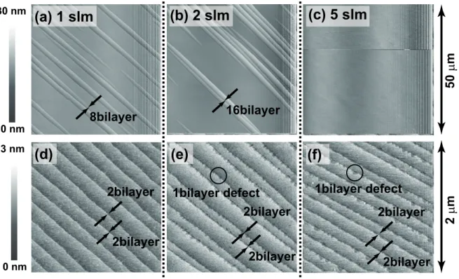
The surface morphologies of 4H-SiC (0001) etched for a temperature range of 1300– 1500◦C are shown in Fig. 3.1. All SiC surfaces were etched, and step-and-terrace structures
were obtained. The steps are parallel and periodic over the SiC surfaces (Fig. 3.1 (d)). The step height was 0.5 nm, corresponding to the half-unit-cell (2 Si-C bilayer) height of the 4H-SiC (0001). The terraces were atomically smooth: RMS roughness was under 0.1 nm. The terrace width was about 200 nm, which corresponds 0.15◦ tilt, indicating the vicinal-off
angle was conserved after gas etching. Below 1400◦C, 2-bilayer-high steps were uniformly
obtained at the large area. The edges of the 2-bilayer-high steps, however, are zigzag due to excess etching with 1-bilayer height (Fig. 3.1 (e)). Si droplets were sometimes observed on the surface by AFM (not shown in the figure). At 1500◦C, huge step bunching was
occurred, composed of 60-bilayer-high steps and 10-µm-wide terraces (Fig. 3.1 (c)). On the wide terraces, two 1-bilayer-high steps and 1-bilayer-high hollows (3 × 109 cm−2) existed
(Fig. 3.1 (f)). No Si droplets were observed on the surfaces at high temperature.
The surface morphologies of 4H-SiC (0001) etched for a pressure range of 1.3 × 10⁴ –
6.7 × 10⁴ Pa are shown in Fig. 3.2. A big step bunching over 16 bilayer was generated in the
low pressure (Fig. 3.2 (a)). In 3.3 × 10³ Pa, the step height was larger than 20 bilayer (not
shown). There were two 1-bilayer-high steps on the terraces, like the etching at 1500◦C.
The 2-bilayer-high steps were achieved in the pressure above 3.3 × 10⁴ Pa.
To avoid excess etching with 1-bilayer height at the step edges, the H2-flow rate and
etching time were also optimized. The surface morphologies of 4H-SiC (0001) etched for a flow rate range of 1–5 slm are shown in Fig. 3.3. The 2-bilayer-high steps were uniformly achieved independently of the flow rate. The higher the flow rate, the larger were the 1-bilayer-high surface defects (Fig. 3.3 (d)-(f)). The surface morphologies of 4H-SiC (0001) etched for 30–60 min are shown in Fig. 3.4. The surface etched for 60 min is only slightly
30 nm 0 nm 3 nm 0 nm 50 µ m 2 µ m
(a) 1300 °C
(b) 1400 °C
(c) 1500 °C
2bilayer 2bilayer 2bilayer 2bilayer 1bilayer defect1bilayer 1bilayer
(d)
(e)
(f)
1bilayer hollow 16bilayer 56bilayer
Figure 3.1: Surface morphologies of 4H-SiC (0001) etched at (a, d) 1300, (b, e) 1400, and (c, f) 1500◦C in H
2 atmosphere. Pressure, H2-flow rate, and etching time were 3.3 × 10⁴ Pa,
2 slm, and 30 min, respectively.
30 nm 0 nm 5 nm 0 nm 5 0 µ m 2 µ m
(a) 1.3×10
4Pa
(b) 3.3×10
4Pa
(c) 6.7×10
4Pa
2bilayer 2bilayer 1bilayer defect1bilayer 16bilayer 1bilayer
(d)
(e)
(f)
2bilayer 2bilayer 20bilayer 16bilayerFigure 3.2: Surface morphologies of 4H-SiC (0001) etched in (a, d) 1.3, (b, e) 3.3, and (c, f) 6.7 × 10⁴ Pa in H
2 atmosphere. Temperature, H2-flow rate, and etching time were
30 nm
0 nm
(a) N-rich AlN growth
3 nm 0 nm 5 0 µ m 2 µ m
(a) 1 slm
(b) 2 slm
(c) 5 slm
2bilayer 2bilayer 2bilayer 2bilayer 2bilayer 2bilayer 1bilayer defect 1bilayer defect(d)
(e)
(f)
16bilayer 8bilayer
Figure 3.3: Surface morphologies of 4H-SiC (0001) etched at H2-flow rate of (a, d) 1, (b,
e) 2, and (c, f) 5 slm in H2 atmosphere. Temperature, pressure, and etching time were
1400◦C, 3.3 × 10⁴ Pa, and 30 min, respectively.
30 nm 0 nm 3 nm 0 nm 5 0 µ m 2 µ m
(a) 30 min
(b) 60 min
2bilayer 2bilayer 1bilayer defect 2bilayer 2bilayer
(d)
(c)
16bilayer 16bilayerFigure 3.4: Surface morphologies of 4H-SiC (0001) etched at (a, c) 30 and (b, d) 60 min in H2 atmosphere. Temperature, pressure, and H2-flow rate were 1400◦C, 3.3 × 10⁴ Pa, and