Optical absorption and emission in the defect-chalcopyrite
semiconductor CdGa
2Te
4Shunji Ozaki,a兲Kei-Ichi Muto, Hisatoshi Nagata, and Sadao Adachi
Department of Electronic Engineering, Faculty of Engineering, Gunma University, Kiryu-shi, Gunma 376-8515, Japan
共Received 4 October 2004; accepted 9 November 2004; published online 21 January 2005兲
Optical-absorption and photoluminescence 共PL兲 spectra have been measured on the defect-chalcopyrite-type semiconductor CdGa2Te4 in the 0.9– 1.5-eV photon-energy range at
temperatures between 11 and 300 K. The temperature dependence of the direct-gap energy of CdGa2Te4 has been determined from the optical-absorption spectra and fit using the Varshni equation and an analytical four-parameter expression developed for the explanation of the band-gap shrinkage effect in semiconductors. The PL spectra show an asymmetric emission band peaking at
⬃1.326 eV and a symmetric emission band at ⬃1.175 eV at T=11 K, which are attributed to
donor-acceptor-pair recombination between exponentially tailed or Gaussian-like donor states and acceptor levels, respectively. A multiple-exponential fit analysis of the PL emission suggests acceptor levels of 50 and 86 meV and a deep donor level of 190 meV, together with an unidentified shallow level of 9 meV. An energy-band scheme has been proposed for the explanation of PL emission observed in CdGa2Te4. © 2005 American Institute of Physics.关DOI: 10.1063/1.1845582兴
I. INTRODUCTION
The ternary semiconducting compounds AIIB2IIIC4VIhave been widely investigated because of their potential applica-tions to electro-optic, optoelectronic, and nonlinear optical devices.1Most of these compounds have defect-chalcopyrite
共space group=S42兲 or defect stannite 共space group=D2d11兲
structure.2CdGa2Te4is one of the defect-chalcopyrite family and is known to have a nearly ideal chalcopyrite structure.3 Although the material has been the subject of many research efforts, many fundamental properties are not sufficiently evaluated or are even unknown.4
Very little is known about the optical properties of CdGa2Te4.
5,6
Paulavichyus et al.5 performed optical reflec-tion, absorpreflec-tion, and photoconductivity measurements on CdGa2Te4films vacuum evaporated on glass substrates. The
optical-absorption edge was determined to be ⬃1.3 eV. Ni-kolić and Stojilković6studied far-infrared reflectivity spectra of bulk CdGa2Te4single crystals in the 40– 400-cm−1
wave-number range at room temperature. The measured spectra were well characterized by a five harmonic-oscillator model. They reported the high-frequency and static dielectric con-stants to be ⬁⬜共s⬜兲=5.73 共12.04兲 and ⬁储共s储兲 = 6.27共11.47兲, respectively, where ⬁⬜共s⬜兲 and ⬁储共s储兲 are the high-frequency 共static兲 dielectric constants for light polarized perpendicular and parallel to the tetragonal axis c, respectively.
In our previous paper7we synthesized bulk polycrystal-line CdGa2Te4crystals and measured their ellipsometric and
electroreflectance spectra. The measured spectra revealed distinct structures at various critical points, and these struc-tures were assigned to specific points in the Brillouin zone by the aid of a band-structure calculation using empirical pseudopotential method. Room-temperature optical
absorp-tion further indicated that CdGa2Te4 is a direct-band-gap
semiconductor having the lowest-direct-gap energy at
⬃1.36 eV.
In this article we present the optical-absorption and pho-toluminescence共PL兲 spectra for CdGa2Te4measured at
tem-peratures T between 11 and 300 K. The temperature depen-dence of the lowest-direct-gap energy Egfor CdGa2Te4will
be determined from the optical-absorption spectra. The de-pendence of Eg on T has been commonly described by the empirical equation proposed by Varshni.8An analytical ex-pression has been recently proposed by Pässler9,10by consid-ering the band-gap shrinkage effect in accordance with gen-eral equations and parameter relationships governing the electron-phonon interaction mechanism. The Egvs T data for CdGa2Te4 will be analyzed using these two expressions. No PL measurement has been carried out on CdGa2Te4 to date. We will observe two PL emission bands peaking at ⬃1.33 and⬃1.18 eV at T=11 K. These emission bands are attrib-uted to transitions from the exponentially tailed or Gaussian-like donor states and acceptor levels, respectively. The expo-nentially tailed donor states may be caused by a large number of donors in the defect-chalcopyrite or stannite semiconductors.1,11
II. EXPERIMENT
The CdGa2Te4crystals used were grown by the conven-tional Bridgman method reported in the previous paper.7 They were polycrystalline with grain size of several mm3.
The hot-probe measurements suggested that the electrical conductivity of the samples is p type. The samples were prepared by cutting the ingot with a wire saw, by mechani-cally polishing, and finally, by chemimechani-cally etching with a solution of Br2 in methanol. Thickness of the samples was ⬃0.1 mm.
a兲Electronic mail: [email protected]
The halogen lamp was used for optical-absorption mea-surements, and the 488.0-nm line of an Ar+-ion laser共NEC GLG3110兲 chopped at 320 Hz was used as the excitation light source for PL measurements. The optical-absorption and PL spectra were taken in the 0.9– 1.5-eV photon-energy range using a grating spectrometer 共JASCO CT-25C兲 and a liquid-nitrogen-cooled Ge photodiode 共Hamamatsu B6175-05兲. The spectral resolution of the grating spectrometer used was about ±0.1 nm共±0.2 meV兲 at the band edge of CdGa2Te4. The measurements were performed using a
closed-cycle refrigerator cryostat共IWATANI CRT105PL兲 be-tween T = 11 and 300 K. Note that the experiments were car-ried out on a few grains of the polycrystalline sample. No attention was, therefore, paid to the polarization dependence of the optical spectra.
III. RESULTS AND DISCUSSION A. Optical-absorption measurements
One of the most important parameters characterizing semiconducting properties is the band-gap energy Eg. In or-der to determine the fundamental band-gap energy of CdGa2Te4, we measured the optical-absorption spectra of the material. The absorption coefficient␣ was determined from the experimental transmittance T using the relation
T =共1 − R兲 2e−␣x
1 − R2e−2␣x, 共1兲
where R is the reflectivity. We used a value of R = 0.25 which was obtained from our previous spectroscopic ellipsometry data.7
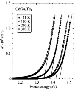
Figure 1 shows the experimental absorption spectra mea-sured at T = 11– 300 K for CdGa2Te4. The dependence of␣
on photon energy E can be written as
␣共E兲 = A共E − Eg兲n, 共2兲
where n = 1 / 2 and 2 correspond to the direct and indirect band gaps, respectively. We found that the fit is superior for
n = 1 / 2 than for 2. The fact suggests that CdGa2Te4may be a
direct-gap semiconductor, in agreement with our band-structure calculation.7 The plots in Fig. 1 give intercepts,
Eg⬃1.44 eV 共T=11 K兲, ⬃1.42 eV 共T=100 K兲, ⬃1.38 eV
共T=200 K兲, and ⬃1.35 eV 共T=300 K兲, on the energy axis.
Traditionally, temperature variation of the band-gap en-ergy is expressed in terms of Varshni’s formula8
Eg共T兲 = Eg共0兲 − ␣T 2
T +, 共3兲
where Eg共0兲 is the band-gap energy at T=0 K,␣is in eV/K, and  is closely related to the Debye temperature of the material共in Kelvin兲. The dashed line in Fig. 2 represents the least-squares fit of the experimental data to Eq. 共3兲. The fit-determined parameter values are listed in Table I.
Recently, Pässler9,10 proposed an analytical expression which takes into account the band-gap shrinkage effect in accordance with general equations and parameter relation-ships governing the electron-phonon interaction mechanism,
Eg共T兲 = Eg共0兲 − ␣p⌰p 2
冋
冑
p 1 +冉
2T ⌰p冊
p − 1册
, 共4兲 where ␣p plays the role of a T→⬁ limiting value of the band-gap shrinkage coefficient −Eg共T兲/T, ⌰p is approxi-mately equal to the average phonon temperature, and the power exponent p is closely related to the overall shape of the electron-phonon spectral function in the given material. This expression is more palatable than Eq.共3兲 from the the-oretical point of view. The solid line in Fig. 2 indicates the FIG. 1. Plots of the square of the absorption coefficient, ␣2, vs photonenergy for CdGa2Te4 at T = 11– 300 K. The intercept point on the energy
axis gives the band-gap energy Egat each temperature.
FIG. 2. Plots of Eg vs T for CdGa2Te4 determined from the
optical-absorption measurements. The dashed and solid lines represent the calcu-lated results of Eqs.共3兲 and 共4兲, respectively. The fit-determined parameters are listed in Table I.
TABLE I. Values of Eg共0兲,␣, andin Eq.共3兲 and those of␣p,⌰p, and p
in Eq.共4兲 for CdGa2Te4.
Eg共0兲 共eV兲 ␣共meV/K兲 共K兲 ␣p共meV/K兲 ⌰p共K兲 p
fitted result of the data to Eq.共4兲. The fit-determined param-eters are listed in Table I. We can see in Fig. 2 that these two equations show an equally good agreement with the experi-mental data in the T = 11– 300-K temperature range.
The effective phonon temperature ⌰p in Eq. 共4兲 is ex-pected to be related to the Debye temperature D by ⌰p
⬃2/3D.
9
The ⌰p value listed in Table I is 58 K. We can, thus, obtainD⬃87 K for CdGa2Te4. NoDvalue has been reported for CdGa2Te4. We can, however, find that the
esti-mated value ofD⬃87 K is smaller or larger than the CdTe values of D⬃158 K at T=0 K and ⬃44 K at T=290 K
共Ref. 12兲, respectively.
Differentiating Eq.共4兲 with respect to T, we obtain
Eg共T兲 T = −␣p
冉
2T ⌰p冊
p−1冋
1 +冉
2T ⌰p冊
p册
共1−p兲/p . 共5兲The temperature coefficient Eg/T for CdGa2Te4 at T
= 300 K obtained from Eq.共5兲 is −0.35 meV/K. NoEg/T value has been reported for CdGa2Te4. However, we can
point out that our obtained Eg/T value is in excellent agreement with that for CdTe共−0.36 meV/K兲.12
B. PL measurements
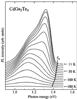
We show in Fig. 3 the PL spectra for CdGa2Te4obtained at temperatures between 11 and 180 K. The vertical arrow indicates the position of the band-gap energy Egat each tem-perature. It is evident from Fig. 3 that at low temperatures, the PL spectra show the dominant emission peak at⬃1.3 eV
共DA1兲 with a shoulder at ⬃1.2 eV 共DA2兲. At temperatures
higher than ⬃120 K, the ⬃1.3-eV emission peak becomes very weak and, as a result, the low-energy shoulder is ob-served only as the single emission peak. No band-edge emis-sion has been recognized in the PL spectra even at low tem-peratures.
The donor-acceptor 共DA兲-pair emission band can be modeled using a Gaussian line shape as
IDA共E兲 = SDAexp
冋
−共E − Ep兲2
⌫2
册
, 共6兲where Epis the DA-pair emission-peak energy, and SDAand ⌫ are the strength and spectral width parameters,
respec-tively.
Figure 4共a兲 shows the fitted result of the experimental PL spectrum measured at T = 11 K 共open circles兲 to Eq. 共6兲 by taking into account the two Gaussian peaks, DA1 and DA2. It is evident from Fig. 4共a兲 that the simple Gaussian line-shape model gives no good agreement with the experi-mental data, especially at both sides of the DA1 emission band共⬃1.33 eV兲.
In order to achieve a better fit with the experimental data, we assume that the density of states in the conduction-band tail of the DA1 emission conduction-band depends exponentially on the energy distance from the unperturbed conduction-band edge13
ND1共E,T兲 =
冦
ND10
1 + A1e−ED1eff/kTexp关m共E − Ed兲兴,E 艋 Ed
0,E⬎ Ed,
冧
共7兲
where ED1eff is the effective共or “center-of-gravity”兲 energy of the exponentially tailed donor states共see Fig. 9, below兲, Edis the so-called “demarcation level” of the donor states, ND10 is the density of donor states at E = Edand T = 0 K, and m is the slope of the conduction-band tail. Here, the ED1eff term is in-troduced in order to take into account the thermal excitation of the exponential donor electrons into the conduction band
共see Fig. 6, below兲. The slope parameter m is assumed to be
independent of T.
The exponentially tailed donor states may arise from the failure in the periodic distribution of the stoichiometric voids in the defect-chalcopyrite structure.11Anedda et al.14 mea-FIG. 3. PL spectra of CdGa2Te4measured at T = 11– 180 K. The vertical
arrows indicate the positions of the band-gap energy Eg.
FIG. 4. Theoretical fit of the PL spectrum for CdGa2Te4measured at T
= 11 K. The dashed lines in共a兲 represent the DA-pair components obtained from Eq.共6兲 共DA1 and DA2兲, while those in 共b兲 are obtained from Eqs. 共10兲
共DA1兲 and 共6兲 共DA2兲. The vertical arrows indicate the position of the
NA1共E,T兲 =
NA1
1 + B1e−EA1/kT
exp
冋
−共E − EA1兲⌫2
册
, 共8兲where NA10 is the acceptor concentration, EA1is the acceptor
ionization energy, and⌫ is the width parameter of the accep-tor states.
As we will see later, the temperature dependence of the PL intensity for the ⬃1.33-eV peak 共DA1 did not show a simple exponential behavior, exp共EA1/ kT兲, defined by an ac-tivation energy EA1of the acceptor states. We found that the
experimental results can be well explained by a double-exponential fit.16 Note that the photogenerated carrier distri-bution in localized states cannot be described by thermal equilibrium conditions. We, therefore, modify Eq.共8兲 by tak-ing into account the double-exponential fit model as16
NA1共E,T兲 = NA1
0
1 + B1e−EA1/kT+ C1e−EX/kT ⫻exp
冋
−共E − EA1兲2
⌫2
册
. 共9兲Note that the double-exponential fit model promises the pres-ence of another acceptor level at an energy EX.
The resultant DA-pair recombination intensity IDA1共E,T兲 can be given by the convolution integral as13
IDA1共E,T兲 = PDA1
冕
NA1共E⬘
,T兲ND1共E⬘
+ E,T兲dE⬘
, 共10兲 where PDA1 is the DA-pair 共DA1兲 transition probabilitywhich is assumed to be independent of E and T. The param-eters ⌫ and Ed influence essentially the peak width and asymmetry of the spectrum, respectively. The m value to be fit determined below is 9.2 eV−1.
Figure 4共b兲 shows the fitted result of the experimental PL spectrum using Eq.共10兲 for the DA1 emission. The con-tribution of the DA2 emission is assumed to be given by Eq.
共6兲. Individual contributions of the DA1 and DA2 emission
bands are shown in Fig. 4共b兲 by the dashed lines. Assuming the exponentially tailed donor density of Eq.共7兲, the theoret-ical calculation begins to show excellent agreement with the experimental data over the entire photon-energy range. Note that this type of luminescence has been commonly found in spectra of defect-chalcopyrite and stannite AIIB
2 IIIC
4 VI
semi-conductors, such as CdGa2Se4, 17 CdIn2Te4, 18 CdIn2S4, 19,20 ZnGa2Se4, 21 ZnIn2S4, 13
and ZnIn2Te4 共Ref. 22兲 共see also
Refs. 1 and 11兲, although no detailed analysis has been per-formed up to date.
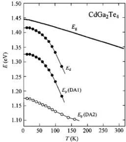
We show in Fig. 5 the temperature dependence of the DA-pair emission energies, Ep共DA1兲 and Ep共DA2兲, and the
demarcation level width Ed for CdGa2Te4. For comparison,
the temperature dependence of Eg is plotted by the heavy solid line. As similar to Eg, Ep共DA2兲 decreases with increas-ing T. Ep 共DA1兲 and Ed, on the other hand, decrease more rapidly than Eg. The temperature coefficients for Ep 共DA1兲 and Ed are found to be about −2.5 meV/ K at T⬃120 K, which is an order larger than that for Eg共−0.35 meV/K, see Fig. 2兲.
The DA-pair emission energy can be theoretically ex-pressed as Ep共T兲=Eg共T兲−EA− ED+共e2/ 4r兲, where r is the
paired DA distance. The lowest possible DA-pair energy is given in the limit r→⬁ by Ep共T兲=Eg共T兲−EA− ED. The
de-pendence of Ep on T may, thus, be very similar to Eg共T兲. Besides the band-structure change induced by thermal ex-pansion of the lattice, the temperature dependence of Eg is known to be mainly due to the electron-phonon interaction.
The temperature coefficients for Epand Ed, −0.2 meV/ K at T⬃150 K, observed in ZnIn2Te4were about twice smaller
than that for Eg 共−0.43 meV/K兲.
22
The very weak tempera-ture dependence of Epin this material resembles deep-center luminescence typically observed in II-VI semiconductors.23 A very shallow localized level, for which the electron orbital extends many interatomic spacing, can be reasonably as-sumed to interact with the host-lattice phonons and the local modes can be neglected. A highly localized deep lumines-cence center as the self-activated center in II-VI semiconduc-tors, on the other hand, can be interpreted by the configura-tional coordinate model. It is unclear that the exponential-donor–acceptor-pair states in defect-type semiconductors are highly localized or not; however, it is likely that they interact not only with the fundamental mode of vibration but also with a number of phonon modes. This may lead to the un-usual temperature dependence of the DA-pair emissions ob-served in CdGa2Te4 共Fig. 5兲, ZnIn2Te4 共Ref. 22兲, and
AgIn5S8共Ref. 24兲.
The demarcation level width Ed in ZnIn2Te4 at T
= 11 K was found to be⬃0.01 eV smaller than Eg.
22
How-ever, its temperature variation was much smaller than that of FIG. 5. Variations of the band-gap energy Eg, demarcation level width Ed,
and DA-pair peak energies Ep’s as a function of temperature T for
Eg and, thus, a crossover occurred between Eg and Ed at T
⬃90 K. Then, for T⬎90 K 共Ed⬎Eg兲 a part of the donor electrons in the demarcation levels can be transferred to the conduction band, resulted in an appearance of the band-edge
共Eg兲 emission 关see Fig. 8共c兲 in Ref. 22兴. On the other hand, no Eg− Ed crossover can be found in CdGa2Te4 over T = 11 and 300 K 共Fig. 5兲. We can, therefore, never observe any band-edge emission in PL of CdGa2Te4共see Fig. 3兲.
The temperature-dependent strength parameter of the DA1 emission can be written from Eqs.共7兲–共10兲 as
SDA1共T兲 = SDA1
0
共1 + A1e−ED1eff/kT兲共1 + B1e−EA1/kT+ C 1e−EX/kT兲
,
共11兲
with
SDA10 = ND10 NA10 PDA1. 共12兲
Similarly, the strength parameter of the DA2 emission can be written as SDA2共T兲 = SDA2 0 共1 + A2e−ED2/kT兲共1 + B2e−EA2/kT兲, 共13兲 with SDA2 0 = ND2 0 NA2 0 PDA2. 共14兲
In Fig. 6, we show the variations of SDA for the DA1 and
DA2 emission bands as a function of temperature T. The solid lines represent the calculated results of Eqs. 共11兲 and
共13兲 with SDA10
= 9.12⫻10−3, A1= 50, B1= 7000, C1= 3.5关Eq. 共11兲兴 and SDA2
0 = 1.65⫻10−4, A
2= 2⫻105, B2= 2800 关Eq. 共13兲兴, respectively. The activation energies determined here
are EA1= 50 meV, EX= 9 meV, and ED1eff= 47 meV关Eq. 共11兲兴;
EA2= 86 meV and ED2= 190 meV 关Eq. 共13兲兴, respectively. The dashed and dotted lines in Fig. 6 are also obtained by putting C1= 0 共i.e., neglecting EX兲 or A1= 0共i.e., neglecting
ED1eff兲 into Eq. 共11兲, respectively. No good agreement can be
achieved between these calculated results and experimental data.
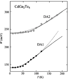
Figure 7 shows the full width at half maximum W for the DA1 and DA2 emission bands as a function of temperature T in CdGa2Te4. One of the important results of the
configura-tional coordinate model is the form of the temperature de-pendence of the emission band width W共T兲 共Ref. 23兲
W共T兲 = A + B
冋
coth冉
បq 2kT冊
册
1/2
, 共15兲
whereបq is the energy of the vibrational mode that inter-acts strongly with the luminescence center in its exited elec-tronic states. The solid lines in Fig. 7 show the calculated results of Eq.共15兲. The fitting parameters are given in Table II. We find that theបqvalue of 23 meV for the DA2 emis-sion is nearly the same as that of the longitudinal-optical
共LO兲 phonons in CdTe 共បLO⬃21 meV, Ref. 12兲, while the បqvalue of 13 meV for the DA1 emission is much smaller than the LO-phonon value in CdTe,បLO⬃21 meV. It is not clear at present where the smallerបqvalue determined for the DA1 emission corresponds to its unique temperature de-pendence of Ep共see Fig. 5兲 or not.
The dashed lines in Fig. 7 represent the fitted results using an expression
W共T兲 = W共0兲 + ␣T 2
T +, 共16兲
where W共0兲 is the T=0-K value. Note that this expression has the same form as the Varshni’s equation of Eq.共3兲. The
W共0兲,␣, andvalues determined here are listed in Table II. It is seen in Fig. 7 that Eq. 共16兲 shows a poorer agreement with the experimental data compared with Eq.共15兲.
FIG. 6. Variations of the strength parameters SDA1and SDA2as a function of
temperature T for CdGa2Te4. The solid lines show the calculated results of
Eqs.共11兲 共SDA1兲 and 共13兲 共SDA2兲, respectively. The dashed and dotted lines
are also calculated from Eq.共11兲 by putting C1= 0共i.e., neglecting EX兲 or
A1= 0共i.e., neglecting ED1 eff
兲, respectively.
FIG. 7. Variations of the spectral widths W for the DA1 and DA2 emissions as a function of temperature T for CdGa2Te4. The solid and dashed lines
represent the calculated results of Eqs.共15兲 and 共16兲, respectively. The fit-determined parameters are listed in Table II.
TABLE II. Values of A, B, andបqin Eq.共15兲 and those of W共0兲,␣, and
in Eq.共16兲 for CdGa2Te4.
A共meV兲 B 共meV/K兲 បq共meV兲 W共0兲 共meV兲 ␣共meV/K兲 共K兲
DA1 7.3 134 13 141 3.6 1000
The PL spectra observed in CdGa2Te4 showed the two
DA-pair emission bands; asymmetric DA1 and symmetric DA2 bands. In order to confirm these two bands as actually due to the DA-pair emissions, we examined the excitation intensity dependence of the PL peak energy and integrated emission intensity at T = 11 K. Figure 8 presents the results of these experiments. It is seen in Fig. 8共a兲 that the DA1
共DA2兲 peak energy Ep increases from 1.302
共1.177兲 to 1.330 eV 共1.209 eV兲 as the laser excitation
inten-sity increases from 0.02 to 2 W / cm2. For the DA-pair re-combination, the excitation laser power Iexcan be expressed,
as a function of PL peak energy Ep, as
24 Iex= I0 共Ep− E⬁兲3 共EB− E⬁− 2Ep兲 exp
冋
−2共EB− E⬁兲 Ep− E⬁册
, 共17兲where I0is a proportionality constant, EBis the emitted pho-ton energy of a close DA pair separated by a shallow-impurity Bohr radius, and E⬁is the emitted photon energy of an infinity distant DA pair. The solid lines in Fig. 8共a兲 rep-resent the fitted results of the experimental Epvalues to Eq.
共17兲. The fit-determined DA1 共DA2兲 parameters are EB = 1.43 eV共1.43 eV兲 and E⬁= 1.25 eV共1.11 eV兲. We can find that these parameters satisfy the DA-pair emission require-ment of E⬁艋Ep= 1.302– 1.330 eV 共Ep= 1.177– 1.209 eV兲
艋EBfor the DA1共DA2兲 emission.
The integrated PL intensity I vs Iexcan be given by the
simple power law24
I⬀ Iex␥. 共18兲
The dimensionless exponent␥ is known to be 1⬍␥⬍2 for free-exciton or bound-exciton emission and␥艋1 for free-to-bound or DA-pair emission. The solid lines in Fig. 8共b兲 rep-resent the fitted results of the experimental data to Eq.共18兲. The␥ values, 1.0共DA1兲 and 0.9 共DA2兲, support the assign-ment of these PL emissions to DA-pair recombination at least for T = 11 K. The relatively strong thermal quenching of the PL intensity is a formidable barrier to make the same assignment at high temperatures.
We finally show in Fig. 9 the schematic energy-band diagram and PL transitions observed in CdGa2Te4 for T
= 11 K. The conduction-band and valence-band density of states can be represented by the well-known expressions of
NC⬀共E−EC兲1/2and NV⬀共EV− E兲1/2, respectively. The expo-nentially tailed donor states of Eq. 共7兲 and broadened Gaussian-like acceptor states of Eq. 共8兲 are also shown in Fig. 9. The acceptor levels determined here are centered at 50 meV 共DA1兲 and 86 meV 共DA2兲 above the top of the valence band, respectively. The double-exponential quench-ing behavior of the IDA1 emission suggests the presence of
another impurity or trap level with an activation of EX = 9 meV.
The PL emission caused by transitions from the expo-nentially tailed or Gaussian-like donor states to acceptor lev-els showed the typical DA-pair recombination characteris-tics, as demonstrated in Fig. 8. It is easy to consider that in the vacancy tetrahedral semiconductors such as CdGa2Te4,
the vacancies in the cation sublattice are the origin of the exponentially tailed donor states and Gaussian-like acceptor levels.14 The photogenerated electrons in the conduction band can be efficiently transferred, via energy relaxation, to the exponential-donor states. The exponential-donor-related emission DA1 is, thus, the dominant PL mechanism in CdGa2Te4. Reflecting the exponentially tailed donor states, the DA1 emission band observed is strongly asymmetric with tail at the low photon-energy side. An intermixing of the exponential and Gaussian donor states共ED2= 190 meV兲 may be the main cause of the large temperature change in Ep
共DA1兲 and its intensity for T艌50 K 共Figs. 5 and 6兲. The
band-to-band emission has never been observed in CdGa2Te4. This is because always Ed⬍Eg in CdGa2Te4. In
ZnIn2Te4, Ed艋Eg for T艋90 K and Ed⬎Eg for T⬎90 K; then, the band-to-band emission was observed only for T
⬎90 K.22
IV. CONCLUSIONS
We have measured the optical-absorption and PL emis-sion spectra on the defect-chalcopyrite-type ternary semicon-FIG. 8.共a兲 Excitation intensity dependence of the PL peak energies Ep’s and
共b兲 integrated PL intensities for the DA1 and DA2 emissions in CdGa2Te4at
T = 11 K. The solid lines in共a兲 and 共b兲 are calculated from Eqs. 共17兲 and
共18兲, respectively.
FIG. 9. Proposed energy-band scheme and optical transitions in CdGa2Te4
ductor CdGa2Te4in the 0.9– 1.5-eV photon-energy range at
T = 11– 300 K. The lowest-direct-gap energy Egof CdGa2Te4 obtained at 11 K and room temperature are ⬃1.44 and
⬃1.35 eV, respectively. The temperature dependence of Eg has been fit using two individual models. The PL spectra have been shown to originate from transitions between the exponentially tailed or Gaussian-like donor states and accep-tor levels. The demarcation level width of Ed= 1.417 eV, a deep donor state located at 190 meV below the bottom of the conduction band, and acceptor levels at 50 and 86 meV above the top of the valence band have also been determined.
1
A. N. Georgobiani, S. I. Radautsan, and I. M. Tiginyanu, Fiz. Tekh. Po-luprovodn.共S.-Peterburg兲 19, 193 共1985兲 关Sov. Phys. Semicond. 19, 121
共1985兲兴. 2
H. Hahn, G. Frank, W. Klingler, A. D. Störger, and G. Störger, Z. Anorg. Allg. Chem. 279, 241共1955兲.
3
S. Ozaki and S. Adachi, Phys. Rev. B 64, 085208共2001兲.
4
O. Madelung, in Landolt—Börnstein: Numerical Data and Functional
Re-lationships in Science and Technology, edited by O. Madelung共Springer,
Berlin, 1985兲, Vol. 17h.
5
A. B. Paulavichyus, V. V. Yasutis, Yu. A. Paukshte, and I. P. Burneika, Litov. Fiz. Sb. 17, 787共1977兲.
6
P. M. Nikolić and S. M. Stojilković, J. Phys. C 14, L551共1981兲. 7
S. Ozaki, K. Muto, and S. Adachi, J. Phys. Chem. Solids 64, 1935共2003兲.
8
Y. P. Varshni, Physica共Amsterdam兲 34, 149 共1967兲.
9
R. Pässler, Phys. Status Solidi B 200, 155共1997兲.
10
R. Pässler, Phys. Status Solidi B 216, 975共1999兲.
11
M. Guzzi and E. Grilli, Mater. Chem. Phys. 11, 295共1984兲.
12
S. Adachi, in Handbook on Physical Properties of Semiconductors, II-VI Compound Semiconductors Vol. 3共Kluwer, Boston, 2004兲.
13
E. Grilli, M. Guzzi, E. Camerlenghi, and F. Pio, Phys. Status Solidi A 90, 691共1985兲.
14
A. Anedda, L. Garbato, F. Raga, and A. Serpi, Phys. Status Solidi A 50, 643共1978兲.
15
P. Manca, F. Raga, and A. Spiga, Nuovo Cimento 19B, 15共1974兲.
16
M. R. Correia, S. Pereira, A. Cavaco, E. Pereira, and E. Alves, Appl. Phys. Lett. 80, 4504共2002兲.
17
G. B. Abdullaev, V. G. Agaev, V. B. Antonov, R. Kh. Nai, and É. Yu. Salaev, Fiz. Tekh. Poluprovodn.共S.-Peterburg兲 6, 1729 共1972兲 关Sov. Phys. Semicond. 6, 1492共1973兲兴.
18
G. Couturier, B. Jean, and J. Salardenne, J. Appl. Phys. 78, 5654共1995兲.
19
E. Grilli, M. Guzzi, P. Cappelletti, and A. V. Moskalonov, Phys. Status Solidi A 59, 755共1980兲.
20
S. Charbonneau, E. Fortin, and J. Beauvais, Can. J. Phys. 65, 204共1987兲.
21
S. I. Radautsan, I. M. Tiginyanu, V. N. Fulga, and Yu. O. Derid, Phys. Status Solidi A 114, 259共1989兲.
22
S. Ozaki, S. Boku, and S. Adachi, Phys. Rev. B 68, 235201共2003兲.
23
See, for example, D. Curie and J. S. Prener, in Physics and Chemistry of
II-VI Compounds, edited by M. Aven and J. S. Prener共North-Holland,
Amsterdam, 1967兲, p. 433.
24
N. M. Gasanly, A. Serpengüzel, A. Aydinli, O. Gürlü, and I. Yilmaz, J. Appl. Phys. 85, 3198共1999兲.